
 ?Mathematical formulae have been encoded as MathML and are displayed in this HTML version using MathJax in order to improve their display. Uncheck the box to turn MathJax off. This feature requires Javascript. Click on a formula to zoom.
Abstract
Carbon nanotube (CNT) shows excellent and novel performances in the field of electrical engineering. The electrical properties of CNT consist of exceptional behaviour that will help to manufacture very tiny semiconductor device. However, due to the lack of research, CNT is still competing with the silicon material in the semiconductor industry. In this research, a single walled CNT wrapping diameter of 1.95 nm is proposed such a way that it performs low energy consumption while it is acting as a channel material of a field-effect transistor. A set of electrical properties of CNT is analyzed to propose a novel model of the nanotube that exhibits low energy consumption compare to other electronics devices. Finally the CNT has been replaced with the silicon in the channel of a field-effect transistor that shows low energy consumption.
Public Interest Statement
In this modern century, electronic gadgets are surrounded over us for our daily life use. It’s true that we need more energy to operate these gadgets. As electronics devices are become miniature, we need to reduce the required energy for these gadgets. In this research we design carbon nanotube (CNT) based transistor which will use low energy compare to the traditional transistor. A single walled CNT wrapping diameter of 1.95 nm is proposed such a way that it performs low energy consumption while it is acting as a channel material of a field-effect transistor. A set of electrical properties of CNT is analyzed to propose a novel model of the nanotube that exhibits low energy consumption compare to other electronics devices. CNT can be best choice by substituting with silicon material.
1. Introduction
Reduction of energy loss in a semiconductor device becomes more challenging task now a day. Miniature size of electronics device is widely expected to everyone. Digital devices become miniature due to small size of the electronics devices.
As the technology grows the demand for scaling down has increased. The CMOS shows various false effects of scaling down. Some of them are short channel effects, hot carrier effect and drain induced barrier lowering (Al-Shaggah, Rjoub, & Khasawneh, Citation2014). Due to these effects a new device has been introduced named carbon nanotube field effect transistor (CNTFET) (Fedawy, Fikry, Alhenawy, & Hassan, Citation2012). One of the most effective technologies is CNTFET is found in the semiconductor industry (Gelao, Marani, Diana, & Perri, Citation2011; Lin, Kim, & Lombardi, Citation2010; Naresh, Singh, Prabhu, Venkataseshaiah, & Sheng, Citation2015). Several researchers have shown excellent performance of CNTFET’s current transport phenomena (Sumanasekera, Adu, Fang, & Eklund, Citation2000; Yao, Kane, & Dekker, Citation2000). The carbon nanotubes (CNT) are formed of graphene sheet. Graphene has advantages of being soft and mechanically strong which make it a suitable component of carbon over diamond for CNT manufacturing (Che, Çagin, & Goddard, Citation2000; Rajendra, Madhavi, & Kishore, Citation2012).
This paper is organized as follows:
| • | Modeling of nanotube is described at section two. | ||||
| • | Implementation and application of the nanotube is described in section three. | ||||
| • | Section 4 shows the results of the proposed work. | ||||
2. Modeling of the tube
2.1. Electrical properties of CNT
To imagine the structure of a CNT you can imagine rolling one sheet of the graphene structure into a tube, the result is a tube that there exist carbon atoms on its surface, and these carbon atoms are arranged in hexagonal patterns. Thus, the structure of CNT directly affects the electrical properties. Based on CNT bandgap, the tube can be acting either metallic or semiconducting behaviour. Here we should note that to consider a unique chiral angle for every nanotube the angle is stated by a value in the region (0, 30°). Using these definitions the diameter of the tube can be computed using the equality of the length of the Ch and the nanotube’s circumference, and finally we can obtain the diameter is defined by,(1)
(1)
where dt is the diameter of nanotube, L is length of the chiral vector, a is basis vector and (n, m) is the chiral vector of a graphene.
The bandgap of a single wall nanotube (SWNT) is defined by,(2)
(2)
where Eg is the band-gap of a nanotube and acc is the distance between carbons.
2.2. Power dissipation
Power dissipation is one of the key challenges for electronics device. Most of the devices are made of CMOS thus power dissipation is a very important topic in the last few years. The number hand-held applications, like the mobile phones and laptops are rapidly increasing and many more additional features are added into the systems, like multi-media applications in handy phones.
| • | As the packet density increases, the need to minimize power dissipation also increases. | ||||
| • | Static power dissipation means the power dissipated when the device is in off state. | ||||
| • | Dynamic power dissipation is the power dissipated when the device is in conduction mode. | ||||
| • | The logic family must have small power dissipation for becoming an efficient device. | ||||
3. Implementation of the tube
3.1. CNTFET PSpice circuit model
Figure shows the equivalent small-signal circuit in PSpice platform. An input current source (Ii) is attached with the gate terminal of the circuit.
Figure 1. The PSPICE equivalent circuit model for CNTFET.
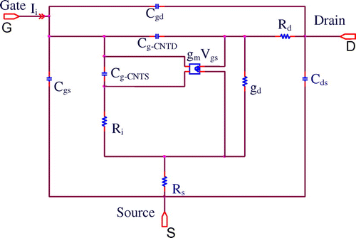
In this equivalent circuit, the gate-drain capacitance is denoted by Cgd. The gate to source capacitance is Cgs where Cds is the drain-source capacitance of the substrate. The channel charging resistance is Ri. Altering the Gate bias, channel is discharged and charged. The voltage of Cg-CNTS controls the dependent current source of gmVgs shorts the voltage across it becomes zero while high frequency is considered for the operation of the device. CNTFET transconductance parameter is gm. The parasitic resistances Rg, Rd, Rs are situated between the contacts.
The circuit proposed in this research is a novel model for nanotechnology devices. Compare to the existing model, the additional part of this circuit is the intrinsic resistance (Ri) which is close to zero value due t avoid short circuit. The quantum capacitances Cg-CNTS, Cg-CNTD are used in this CNTFET circuit model which require very low operating current as low as 0.2 V compare to the other transistors. Furthermore, the power consumption of this model is able reduced as well.
3.2. Circuit level simulation
In this work PSpice was used for coding and simulation. The simulation is carried out on 32 nm technology for MOSFET and 14 nm CNTFET 1 V of power supply. The PSpice circuit model is representing P type CNT in the conductive channel of the transistor. The current driving capability of P-CNTFET is 50% of MOSFET.
4. Results and discussions
4.1. Nanotube physics
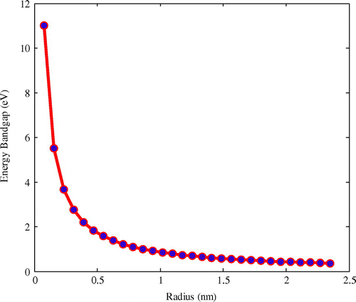
The device physics of graphene was reported in past researches (Farhana, Alam, Khan, & Motakabber, Citation2013; Farhana, Alam, Motakabber, & Khan, Citation2013) in developing the CNT. However, the chiral vector relation of device physics is used in this research to configure the nanotube structure for the further development. Figure shows bandgap vs. radius for semiconducting (zigzag) nanotubes according to electrical properties of CNT. The bandgap decreases inversely with increase in diameter. From the analysis we set the bandgap CNT at (25, 0) semiconducting chirality. Therefore, the diameter of single walled CNT was calculated to 1.95 nm.
Figure 2. Band gap vs. radius for zigzag nano tube.
4.2. CNTFET in logic gates
The design of digital circuit model, inverter is a primary logic gate. Numerous fundamental ideology engaged in the modeling and analysis of logic gate inverter may also be useful to multipart logic gates such as NAND, NOR and XOR. The ratio of N-transistor or P-transistor is necessary for the performance comparison of the CNTFET and MOSFET inverters. Generally the ratio of NMOS and PMOS is 3 or 2 is used, the reason is 3 or 2 times higher mobility value of NMOS than the PMOS. The ration of NMOS and PMOS is 1:3 is involved in this simulation for the MOSFET in 32 nm and CNTFET in 14 nm technology.
On the other hand, the similar current operating capabilities of NCNTFET and PCNTFET enable to take their ratio as 1 within common transistor geometry. The MOSFET width adjusted to modify the NMOS and PMOS ratio in CMOS design. Conversely in CNTFET, the current and resistance will change depends on the changing number of tubes. Therefore, the increment of number of tube will results the increment of the CNTFET width.
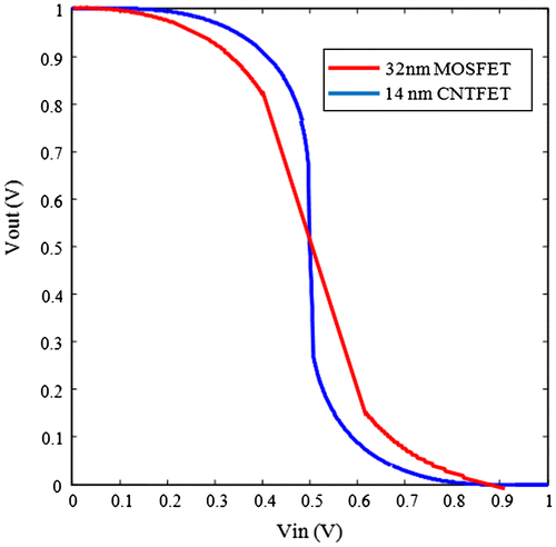
Figure shows the input/output voltage characteristic for 14 nm CNTFET and 32 nm MOSFET to investigate the inverter characteristics. The symmetric curve shows the logic threshold voltage is the half of the input voltage which is obtained at the center of the curve. CNFET performs a steeper bend in the transition zone although the CNTFET’s current quantity is minor than for the small dimension of MOSFET.
Figure 3. The 14 nm CNTFET and 32 nm MOSFET’ transfer curve for input/out voltage characteristic.
4.3. Transistor leakage current
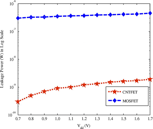
Band to band tunneling leakage current is the main factor of a CNTFET due to the band gap of the CNT transistors. Generally, the average CNTFET based gates leakage power is 150 times lower than the than the MOSFET in logic gates. In addition, low power is required to operate CNTFET logic gate devices compare to MOSFET device. The proposed CNTFET model based logic gate will be able operated as low as 0.2 V while the MOSFET logic gate will unable to operate at this low voltage. Figure shows the average leakage power of the CNTFET and MOSFET inverter at the range of the operating voltage of 0.7–1.7 V. Once the power supply voltage is decreased until the leakage also decreased. In this operation, the CNTFET inverter leakage current is found much smaller than the leakage current for MOSFET inverter. Therefore, selection of the CNTFET in a logic gate device will be the better choices compare to MOSFET based logic gate device.
Figure 4. The inverter leakage power curve using 14 nm CNTFET and 32 nm MOSFET.
4.4. Logic gate power delay product
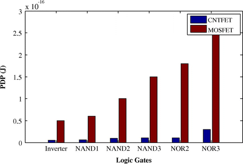
Reducing the power consumption and time delay are difficult challenges in the high speed electronics devices. High power consumption is obtained from a quicker energy transfer. The CNFET and MOSFET performances will be evaluated with the power delay product (PDP).
The PDP of 14 nm of CNTFET and the 32 nm MOSFET inverter logic gate is shown in Figure . It is observed from the Figure that CNTFET inverter is almost 100 times faster than the MOSFET inverter. Also a set of NAD and NOR gate also simulated to verify the PDP using CNTFET and MOSFET as shown in Figure . From the comparison within the CNTFET and MOSFET logic gates, it is confirmed that the CNTFET-based logic gate is better option in electronics industry to manufacture the digital devices.
Figure 5. The PDP of 14 nm CNFET and 32 nm MOSFET based different logic gates.
5. Conclusion
The analysis of this work shows the feasibility of CNT is higher than the other semiconductor material. Geometrical structure of the graphene made CNT is more optimum in its size and functionality as it is shown here that Chirality of (25, 0) of a single walled nanotube able to reduce energy loss of CNTFET. The proposed CNTFET was tested on several logic gates, such as inverter, AND, OR gate. The comparison was successfully performed with the existing silicon MOSFET in the market. Though CNT is used as the channel material here but it is not limited to FET only it can be replaced with silicon in other material also.
Additional information
Funding
Notes on contributors
Soheli Farhana
Dr Soheli Farhana serves as Post-Doctoral Fellow at International Islamic University Malaysia (IIUM). Her research focuses on the development of new nano electronic devices to advance the fields of information technology and biosensors. She is especially interested in the nanotechnologies and novel devices concepts. Since 2015, Dr Soheli has been leading the development of new applications for CNT-based materials in FET application. In 2016, she started research on Nano Technology based software development at IIUM. She is serving as editorial member and committee member in international journals and conferences. Dr Soheli is also the executive committee member of IEEE Nanotechnology council and Systems, Man, and Cybernetics Society (SMC) in Malaysia. She awarded with best student in her PhD research at IIUM. Dr Soheli studied Electrical and Computer Engineering at the International Islamic University Malaysia and received her PhD (Engineering) in 2016.
References
- Al-Shaggah, A., Rjoub, A., & Khasawneh, M. (2014). Impacts of parameter scaling for low-power applications using CNTFET (carbon nanotube field effect transistor) models: A comparative assessment. Journal of Energy and Power Engineering, 8, 1142–1152.
- Che, J., Çagin, T., & Goddard, III, W. A. (2000). Thermal conductivity of carbon nanotubes. Nanotechnology, 11, 65.10.1088/0957-4484/11/2/305
- Farhana, S., Alam, A. Z., Khan, S., & Motakabber, S. M. A. (2013, August). Modeling of optimum chiral carbon nanotube using DFT. In Nanotechnology (IEEE-NANO), 2013 13th IEEE conference on (pp. 853–857). IEEE.
- Farhana, S., Alam, A. Z., Motakabber, S. M. A., & Khan, S. (2013, January). Analysis of CNT electronics structure to design CNTFET. In Nanoelectronics Conference (INEC), 2013 IEEE 5th International (pp. 329–332). IEEE.
- Fedawy, M., Fikry, W., Alhenawy, A., & Hassan, H. (2012, November). IV characteristics model for ballistic single wall carbon nanotube field effect transistors (SW-CNTFET). In Electronics design, systems and applications (ICEDSA), 2012 IEEE international conference on (pp. 10–13). IEEE.10.1109/ICEDSA.2012.6507775
- Gelao, G., Marani, R., Diana, R., & Perri, A. G. (2011). A semiempirical SPICE model for n-type conventional CNTFETs. IEEE Transactions on Nanotechnology, 10, 506–512.10.1109/TNANO.2010.2049499
- Lin, S., Kim, Y. B., & Lombardi, F. (2010). Design of a CNTFET-based SRAM cell by dual-chirality selection. Nanotechnology, IEEE Transactions on, 9, 30–37.
- Naresh, B. N., Singh, A. K., Prabhu, C. M. R., Venkataseshaiah, C., & Sheng, G. C. (2015). Compact analytical model for one dimensional carbon nanotube field effect transistor (CNTFET). ECS Solid State Letters, 4, M12–M14.
- Rajendra, P., Madhavi, B. K., & Kishore, K. L. (2012). Design of low-leakage CNTFET SRAM cell at 32 nm technology using forced stack technique. International Journal of Engineering Research and Applications, 2, 805–808.
- Sumanasekera, G. U., Adu, C. K. W., Fang, S., & Eklund, P. C. (2000). Effects of gas adsorption and collisions on electrical transport in single-walled carbon nanotubes. Physical Review Letters, 85, 1096.10.1103/PhysRevLett.85.1096
- Yao, Z., Kane, C. L., & Dekker, C. (2000). High-field electrical transport in single-wall carbon nanotubes. Physical Review Letters, 84, 2941.10.1103/PhysRevLett.84.2941