 ?Mathematical formulae have been encoded as MathML and are displayed in this HTML version using MathJax in order to improve their display. Uncheck the box to turn MathJax off. This feature requires Javascript. Click on a formula to zoom.
Abstract
A novel compact rectifier for dual-band operation in the RF energy harvesting is presented. The circuit comprises a 4th order dual-band impedance matching and a single-series circuit with one double diode, both are integrating into a compact shape to occupy a small area of . The merit of the proposed rectifier circuit is that it can be extended to n number of the frequency band by using only
matching elements. To validate the design method experimentally, a prototype of a dual-band rectifier is fabricated for two public telecommunication bands of GSM-900 and 1800. In order to reduce the circuit complexity and sensitivity arising due to lumped elements, the meander line and the open stub are used to realize the proposed circuit. A good agreement is obtained between the simulation and the measurement. The measured results show that the proposed rectifier circuit exhibits the conversion efficiency of 25.7 and 65% for an input power of
and 0 dBm, respectively. In addition, diode nonlinearity which affects the performance of the rectifier in terms of impedance matching is also investigated.
Public Interest Statement
With rapid growth in wireless communication, a huge amount of radio frequency (RF) energy broadcasted through billions of microwave sources such as mobile phones, handheld radios, and radio broadcast stations. Therefore, it is meaningful to collect and supply it to many electrical devices like mobile headsets, wearable medical sensors through RF energy harvesting. Since the ambient RF energy is distributed in multiple frequency bands, therefore the amount of energy harvested could increase if the circuit is designed for multiple frequency bands. In this work, we present a compact dual-band energy harvesting circuit to harvest energy from two most useful frequency bands, GSM-900 and 1800. The merit of the proposed rectifier circuit is it can be extended to n number of the frequency band by using only matching elements. A prototype is fabricated, and its performance is evaluated using Vector Network Analyzer (VNA). The total size of the rectifier is about
.
1. Introduction
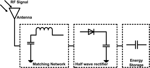
A revolutionary growth in wireless technology attracts huge attention from research community to make the self-sustainable device feasible through RF energy harvesting. It exploits ambient electromagnetic energy transmitted from different RF systems to remotely feed the electronic devices (Nintanavongsa, Muncuk, Lewis, & Chowdhury, Citation2012). Compared to other harvesting techniques, RF energy harvesting provides relatively predictable energy supply owing to the features of easy availability and less dependency on environmental variations. The typical block diagram of RF energy harvesting circuit is shown in Figure . It consists of three major blocks viz; antenna, matching network (MN), diode detector followed by an energy storage. The first element, antenna is employed to capture the RF signals of different frequencies and polarization, while second MN is for maximum power transfer, and the last rectifier is used to convert the RF energy to dc voltage. It means harvesting circuit performance can be evaluated in terms of accessible ambient RF energy and its conversion rate (Agrawal, Pandey, Singh,& Parihar, Citation2014). These parameters are heavily influenced by surrounding terrain conditions as the multiple reflection and dissipation certainly deteriorate the level of available ambient RF energy. As a result, conversion efficiency and dc output voltage may degrade. Previously, the majority of available RF energy harvesting circuits focused on single frequency band hence offer low dc output voltage. As the multiple RF energy sources of different frequency bands are available, thus from an ambient RF harvesting perspective, the output dc voltage could be increased if the circuit is designed for multiple frequency bands rather than a single band. A wide-band energy harvester can also promise a high output voltage by accumulating the number of RF signals at a time. However, due to nonlinear behavior of the diode, harvesting circuit itself exhibits nonlinearity i.e. its input impedance varies with the received RF power. Thus, it is quite difficult to retain the impedance match and high conversion efficiency over a large frequency range (Song, Huang, Zhou, & Carter, Citation2014). The losses due to impedance mismatch over a large bandwidth can be illustrated in Collado and Georgiadis (Citation2013), where only 8% conversion efficiency is achieved at dBm.
To address this, it is preferable to harvest energy from several narrow frequency bands rather than a single large one. In literature, numerous topologies have been proposed to accomplish the multiband energy harvesting (Bergès, Fadel, Oyhenart, Vigneras, & Taris, Citation2015; Hamano et al., Citation2016; Ho et al., Citation2016; Keyrouz, Visser, & Tijhuis, Citation2013; Kuhn, Lahuec, Seguin, & Person, Citation2015; Liu, Zhong, & Guo, Citation2015; Niotaki, Georgiadis, Collado, & Vardakas, Citation2014; Pinuela, Mitcheson, & Lucyszyn, CitationJuly 2013; Scheeler, Korhummel, & Popovic, Citation2014; Shariati, Rowe, Scott, & Ghorban, Citation2015; Sun, Guo, He, & Zhong, Citation2013). These topologies can be differentiated in terms of filter functionality i.e. how the antenna or source impedance is matched to the rectifier circuit. For instance, in Pinuela et al. (CitationJuly 2013) and Keyrouz et al. (Citation2013) several single-band rectennas (combination of antenna and rectifier circuit) were stacked to constitute a multi-band harvesting circuit. In this case, each rectenna was designed for a specific frequency band. Thus, for compact applications, this architecture is not suitable due to the number of antennas used. Moreover, in most of the reported works, the quality assessment of the output voltages combination was not taken into consideration. In Kuhn et al. (Citation2015), the circuit complexity is reduced to a certain extent by replacing the multiple antennas with a single wide-band antenna. However, in this topology too, the number of rectifiers increases with the frequency bands, which leads to prolonging the circuit complexity.
Besides, a multi-band harvesting circuit can also be formed by simply embedding a multi-band matching network between the multi-band antenna and the rectifying circuit (Bergès et al., Citation2015; Hamano et al., Citation2016; Ho et al., Citation2016; Liu et al., Citation2015; Niotaki et al., Citation2014; Scheeler et al., Citation2014; Shariati et al., Citation2015; Sun et al., Citation2013). The multi-band matching network can be designed either by distributed or by lumped element. In general, the multi-band rectifier circuit experiences two types of losses: first due to shift in resonance frequency from the optimum frequency point, and second due to the filter complexity. Because of the diode nonlinearity, the input impedance of the circuit varies as a function of power and frequency which causes a shift in resonance frequency. The difficulty due to diode nonlinearity can be observed in Sun et al. (Citation2013) where the dual-band rectifier circuit exhibits impedance matching for a small range of input power. The losses induced because of filter complexity can be observed in the recently reported works on dual band harvesting circuit (Niotaki et al., Citation2014; Scheeler et al., Citation2014; Shariati et al., Citation2015). In Niotaki et al. (Citation2014), for dBm, author achieved the conversion efficiency of 23% at the expense of increased filter complexity consisting two series and two shunt pairs of reactive elements. Thus, for more than dual band applications, the proposed circuit topology is not suitable due to excessive filtering components used. To obtain good conversion efficiency a dual-band rectenna reported in Scheeler et al. (Citation2014). However, the rectenna was large in size and requiring a complex impedance tuning circuit. In Shariati et al. (Citation2015) also, a dual-band matching network consisting nine reactive elements was employed to achieve the dual-band characteristics.
In order to reduce the filter complexity, this work proposed a compact dual-band harvesting circuit for GSM-900 and 1800. It consists of a 4th order dual-band matching network based on frequency transformation, which is optimized for the energy harvesting circuit to reduce the complexity up to
reactive elements (n is the number of frequency bands). Similar to frequency transformation method, the proposed dual-band rectifier circuit can be extended to n number of frequency bands by using the
number of reactive elements. The detailed analysis and design guidelines of dual band rectifier circuit are discussed in Section 2.
2. Dual band rectifier design and analysis
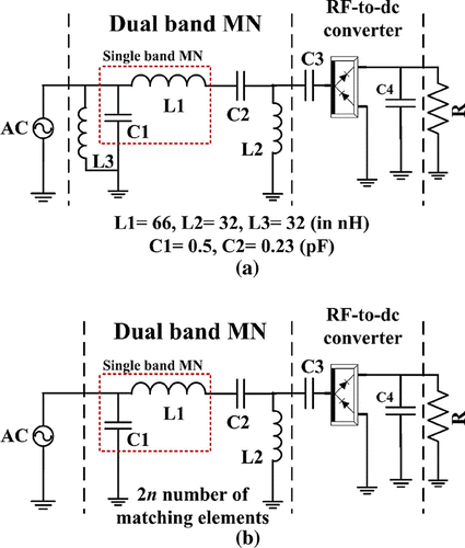
This section presents the design and analysis of a dual-band harvesting circuit in terms of impedance matching, DC output voltage and RF-to-dc conversion efficiency. The topology of the proposed dual-band RF energy harvesting circuit is shown in Figure (a). As seen, the low-cost Schottky diode is used to transform the input RF power to DC voltage. The impedance matching at two frequency is achieved using a series and parallel combination of the LC pair. The main idea underlying the suggested multi-band matching network is frequency transformation (one to many mapping of frequency), which transforms a single-band matching network to multi-band matching network (Nallam & Chatterjee, CitationJune 2013). As the name (
) suggests that for designing a multi-band matching network, primarily a single-band matching network is required whose resonant frequency is dependent on the frequencies for which multi-band matching network proposed to designed.
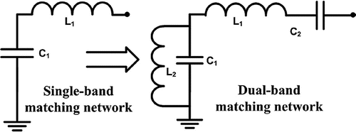
Figure 3. Conversion of a single-band matching network to dual-band matching network using frequency transformation.
Moreover, this frequency transformation method depends on the type of load impedance, whether it is series or parallel combination of RC or RL. Since the selected diode (HSMS-2852) has capacitive behavior throughout the frequency, it can be represented in a series or parallel combination of R and C. In the case of parallel RC load, the following equations are used to transform the single-band matching network into multi-band matching network.(1)
(1)
where, n is the number of bands and m varies from 2 to n. After substituting the value of n, Equation (1) can be expanded in partial fraction form using the causal foster analysis as:(2)
(2)
The coefficients and
can be calculated as:
(3)
(3)
(4)
(4)
(5)
(5)
(6)
(6)
(7)
(7)
Equation (6) is similar to that presented in Nallam and Chatterjee (CitationJune 2013), except the term , which is included here to realize the multi-band matching network for more than three frequency bands i.e. for
.
With this transformation, the capacitor of the matching network is transformed to the combination of prototype capacitor parallel with inductor whereas, an inductor is transformed into a combination of the same inductor with a series capacitor. Figure shows the circuit schematic of transformation of a single-band matching network to the dual-band matching network. It can be seen that is transformed to
and
transformed to
series with
. After successful usage of (1)–(7), the resultant multi-band matching network requires
and
reactive elements for L and
-type topology, respectively.
As the aim is to design a dual-band harvesting circuit, therefore, we require here only 5 or 7 reactive elements with L and -type topologies, respectively. From Figure (a), it can be seen that the resultant matching network consists of five elements, where the inductor
and capacitor
results after the transformation of capacitor
and inductor
, respectively. Besides, the inductor
occurrs due to the diode reactive element, which is generally a capacitor.
In this work, two frequencies 0.9 and 1.8 GHz that correspond to the maximum signal strength are chosen for dual-band harvesting circuit. According to this method, it is necessary to assign the frequencies in descending order e.g. ,
. Therefore, from (3) single-band matching network frequency is equal to
. In order to match the source impedance with the rectifier at the calculated frequency 0.9 GHz, the chosen matching topology is L-type as shown by the encircled portion in Figure (a). The corresponding element values can be approximated using the various methods some of which are described in Pozar (Citation2010). Subsequently, this single-band matching network is transformed to dual-band matching network using (1)–(7). The detailed design steps of the dual-band rectifier circuit are summarized as follows:
| (1) | As we are interested in matching the diode to 50 | ||||
| (2) | In the first step, single-band matching network is designed at the frequency f calculated as: | ||||
| (3) | Afterwards, this single-band matching network is transformed into dual-band using the (1)–(7) as shown below: | ||||
From (4) can be calculated as:
(9)
(9)
(10)
(10)
Thus, inductor (=66 nH) is transformed to impedance as:
(11)
(11)
Similarly, capacitors (=0.5 pF) are transformed to the admittance as:(12)
(12)
The circuit schematic of the dual-band harvesting circuit is shown in Figure (a). It can be seen that resultant matching network consists of five reactive elements according to . In order to reduce the circuit complexity and sensitivity due to reactive elements, a parametric study has been carried out to eliminate the elements showing minimum influence on the circuit performance.
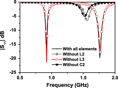
Figure shows the simulated for the different combination of matching elements. The simulated results demonstrate that
experiences maximum change when inductor
and capacitor
are removed from the circuit, whereas it remains almost unaffected when
is not present in the circuit. Therefore, inductor
can be extruded from the circuit and the resultant matching circuit requires only 2n and 3n reactive elements in place of
and
elements. In this way, for each topology, the proposed circuit reduces
elements compared to the conventional method. Figure (b) demonstrates the optimized circuit diagram of the dual-band rectifier. It can be observed that circuit requires large inductors value of 32 and 66 nH. Thus, it is quite difficult to realize the practical rectifier circuit whose response is similar to the response of simulated result. In order to avoid any impedance mismatch due to the small difference in elements value, the meander line inductor and open stub are used to realize the inductors and capacitors, respectively. In this case, not only fabrication and optimization process become so easy but the cost will also reduced.
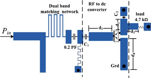
Figure , shows the layout of the dual-band rectifier circuit. In Nintanavongsa et al. (Citation2012) and Agrawal et al. (Citation2014), it has been demonstrated that the number of rectifying diodes or equivalently voltage multiplier stages are very much sensitive to the RF-to-dc conversion efficiency. In low-power region ( dBm), efficiency decreases if voltage multiplier stages increase, whereas in higher power region (
dBm), an opposite effect occurs. As the demand is to harvest energy in low-power region, single-series circuit with a double diode is used to convert received RF energy into dc voltage. From the left side of the circuit, the first meander line corresponds to the inductor
, while the second meander line represents the inductor
, of the Figure (b). The shunt stub is accounted for the shunt capacitor
of Figure (b). The dimensions of each element are calculated according to their respective reactive element value and the substrate on which circuit has to be fabricated. In Assimonis, Daskalakis, and Bletsas (Citation2016), it has been demonstrated that traces (microstrips) connected to the rectifier terminals (e.g. distance between the diode and via and diode and load) are highly sensitive for RF-to-dc efficiency. Therefore, traces
,
between diode and capacitor
and
,
between diode and load and
between diode and ground are adjusted to optimize the impedance matching as well as the conversion efficiency of the rectifier. Due to nonlinear behavior of the diode, harvesting circuit itself exhibits nonlinearity i.e. its input impedance varies with received RF power, therefore harmonic-balance (HB) and large signal analysis (LSSP) were employed to take into consideration the nonlinear behavior of the rectifier.
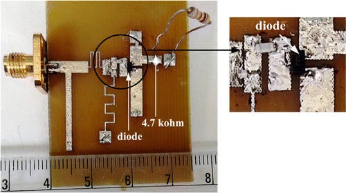
The photograph of the fabricated dual-band rectifier is shown in Figure . It is fabricated on a 1.54 mm thick FR-4 substrate with a dielectric constant () of 4.3 using chemical etching method. The rectifier performance is evaluated in terms of
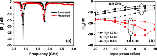
and output voltage using the Agilent vector network analyzer (VNA). The simulated and measured
is illustrated in Figure (a). The measured result shows reasonable agreement with the simulated one; the slight difference can be accounted for the fabrication imperfections. It is well known that impedance matching is a function of frequency and input power, due to the nonlinearity of the diode. Such a characteristic is examined in Figure (b), where the measured
is demonstrated as a function of input power level for three different load impedance values. From results, it is clear that impedance matching of the harvesting circuit is greatly affected by the input power and the load impedance. Figure (b) demonstrates that as power increases, the impedance matching at 0.9 GHz degraded drastically, while at 1.8 GHz, it improves. Moreover, it is noticed that the impedance matching at higher power level is more sensitive to the variation of load impedance (RL).
The measured RF-to-dc conversion efficiency and output voltage vs. input power for both frequencies are demonstrated in Figure (a). For 0.9 GHz, efficiency is equal to 25.7 and 65.1% for an input power of and 0 dBm, respectively. However, at 1.8 GHz the efficiency is relatively small that might be due to the increased parasitic losses in the rectifier diode. Figure (b) shows the relation between the output voltage and frequency for various input power levels at fixed load resistance value of 4.7 k
. It can be seen that maximum output voltage is achieved in the frequency range of 860–900 and 1770–1800 MHz, showing the rectifier’s capability to harvest RF energy in the GSM-900 and 1800 bands.
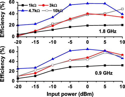
Figure , depicts the measured conversion for various values of load resistance. It can be noticed that the circuit yields maximum efficiency when the load impedance is 4.7 k. It starts decreasing as the load impedance varies from 4.7 k
. Table shows the comparison of the conversion efficiency and the size of the proposed rectifier with the similar works reported previously. Only measured results are compared in Table . It can be seen that in low-power condition maximum efficiency is achieved in Sun et al. (Citation2013), but the expense of bulky circuit size. However, the proposed rectifier offers an optimal conversion efficiency with compact circuit size.
Figure 8. (a) Measured output dc voltage and RF-to-dc conversion efficiency and (b) measured dc voltage vs. frequency.
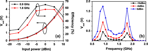
Table 1. Performance comparison of the proposed dual rectifier with recently published works
3. Conclusion
A new compact 4th order dual-band rectifier has been designed to harvest the RF power of GSM-900 and 1800 bands. In order to reduce the circuit complexity and sensitivity due to reactive elements, the meander line and the open stub are used to fabricate the matching network. For dBm, the measured RF-to-dc conversion efficiency of 27.5 and 20% is achieved at 0.9 and 1.8 GHz, respectively. Further, more than 45 and 34% conversion efficiency is maintained from
to 10 dBm for 0.9 and 1.8 GHz, respectively.
Additional information
Funding
Notes on contributors
Sachin Agrawal
Sachin Agrawal did his BE and ME from Jiwaji University and Birla Institute of Technology Pilani, India in 2005 and 2009, respectively. Currently, he is pursuing his PhD from PDPM-Indian Institute of Information Technology Design and Manufacturing Jabalpur, India. His area of interest are; RF energy harvesting circuit, Antenna including planar and dielectric resonator antenna and Power amplifier.
References
- Agrawal, S., Pandey, S. K., Singh, J., & Parihar, M. S. (2014). Realization of efficient RF energy harvesting circuits employing different matching technique (pp. 754–761). Fifteenth International Symposium on Quality Electronic Design, Santa Clara, CA.
- Assimonis, S. D., Daskalakis, S. N., & Bletsas, A. (2016). Sensitive and efficient rf harvesting supply for batteryless backscatter sensor networks. IEEE Transactions on Microwave Theory and Techniques, 64, 1327–1338.
- Bergès, R., Fadel, L., Oyhenart, L., Vigneras, V., & Taris, T. (2015). A dual band 915MHz/2.44 GHz RF energy harvester. Microwave Conference (EuMC), 2015 European. IEEE.
- Collado, A., & Georgiadis, A. (2013). Conformal hybrid solar and electromagnetic (EM) energy harvesting rectenna. IEEE Transactions on Circuits and Systems I: Regular Papers, 60, p. 10.
- Hamano, K., Tanaka, R., Yoshida, S., Miyachi, A., Nishikawa, K., & Kawasaki, S. (2016). Design of dual-band rectifier using microstrip spurline notch filter. Radio-Frequency Integration Technology (RFIT), 2016 IEEE International Symposium on. IEEE.
- Ho, D. K., Kharrat, I., Ngo, V. D., Vuong, T. P., Nguyen, Q. C., & Le, M. T. (2016). Dual-band rectenna for ambient RF energy harvesting at GSM 900 MHz and 1800 MHz (pp. 306–310). 2016 IEEE International Conference on Sustainable Energy Technologies (ICSET), Hanoi.
- Keyrouz, S., Visser, H., & Tijhuis, A. (2013, April). Multi-band simultaneous radio frequency energy harvesting. In Antennas and Propagation (EuCAP), 2013 7th European Conference on, 3058–3061.
- Kuhn, V., Lahuec, C., Seguin, F., & Person, C. (2015). A multi-band stacked RF energy harvester with RF-to-DC efficiency up to 84\%. IEEE Transactions on Microwave Theory and Techniques, 63, 1768–1778.
- Liu, Z., Zhong, Z., & Guo, Y.-X. (2015). Enhanced dual-band ambient RF energy harvesting with ultra-wide power range. IEEE Microwave and Wireless Components Letters, 25, 630–632.
- Nallam, N., & Chatterjee, S. (2013, June). Multi-band frequency transformations, matching networks and amplifiers. Circuits and Systems I: Regular Papers, IEEE Transactions on, 60, 1635–1647.
- Nintanavongsa, P., Muncuk, U., Lewis, D., & Chowdhury, K. (2012, March). Design optimization and implementation for rf energy harvesting circuits. IEEE Journal on Emerging and Selected Topics in Circuits and Systems, 2, 24–33.
- Niotaki, K., Georgiadis, A., Collado, A., & Vardakas, J. S. (2014). Dual-band resistance compression networks for improved rectifier performance. IEEE Transactions on Microwave Theory and Techniques, 62, 3512–3521.
- Pinuela, M., Mitcheson, P., & Lucyszyn, S. (2013, July). Ambient rf energy harvesting in urban and semi-urban environments. Microwave Theory and Techniques, IEEE Transactions on, 61, 2715–2726.
- Pozar, D. M. (2010). Microwave engineering (3rd ed.). New Delhi: Wiley.
- Scheeler, R., Korhummel, S., & Popovic, Z. (2014). A dual-frequency ultralowpower efficient 0.5-g rectenna. IEEE Microwave Magazine, 15, 109–114.
- Shariati, N., Rowe, W. S., Scott, J. R., & Ghorban, K. (2015). Multi-service highly sensitive rectifier for enhanced RF energy scavenging. Scientific Reports, 5, 9655
- Song, C., Huang, Y., Zhou, J., & Carter, P. (2014). Improved ultrawideband rectennas using hybrid resistance compression technique. IEEE Transactions on Antennas and Propagation, 65, 2057–2062.
- Sun, H., Guo, Y. X., He, M., & Zhong, Z. (2013). A dual-band rectenna using broadband Yagi antenna array for ambient RF power harvesting. IEEE Antennas and Wireless Propagation Letters, 12, 918–921. doi:10.1109/LAWP.2013.2272873.

