
 ?Mathematical formulae have been encoded as MathML and are displayed in this HTML version using MathJax in order to improve their display. Uncheck the box to turn MathJax off. This feature requires Javascript. Click on a formula to zoom.
Abstract
The current monolithic integrated circuits revolution has been growing over past few decades, but the VLSI industry faces problems in the domain of short channel effect, device density, and scaling along with power consumption. Hence research is a need to investigate alternative nanoelectronics technology such as Quantum-dot cellular automata (QCA). This paper presents a novel reversible gate with a parity-preserving property realized using QCA technology. Results demonstrate that the proposed gate is more efficient compared to the existing parity-preserving reversible gate designs regarding the area, delay, and power consumption. To facilitate online fault detection of the proposed gate, two new reversible parity generator and parity checker circuits are proposed. The proposed even parity generator succeeded in achieving 62.5% cell count, and 23.07% area from prior works. These two circuits are designed using a new ultra-efficient exclusive-OR (XOR) gate, designed with only 11 cells with an area of 0.02 μm2. We also present an efficient fault-tolerant reversible D-latch using the proposed gate. The QCADesigner and HDLQ tools are used for designing the QCA layouts and for the functional verification of the proposed circuits, respectively. Energy dissipation analysis of the proposed gate is performed using the QCAPro simulation tool.
Public Interest Statement
There has been an unprecedented development in the field of reversible computing during last few decade. In the view of the increased importance of reversible circuit, an energy free computation is considered. Moreover, the reversible operation does not change in entropy and energy to heat during computation. The essence of QCA for reversible circuit design must be accessible to the new computing paradigm and attention to the new generation designer. The QCA cells are designed towards molecular dimensions and smaller size area. This article presents the nanocircuit implementation of reversible circuits such as parity generator and checker, and D-latch which has an inherent potential such as less QCA primitives. Further, it also draws new research being appeared into by this article such as an efficient gate, 13 standard benchmark Boolean functions, QCA computing paradigm of nanocircuits and fault-tolerant of a new gate in QCA creates this architecture in a bottom-up fashion.
1. Introduction
Concept regarding deep-sub-micron in CMOS has faced a challenge due to further scaling. The scaling is a limitation of channel length to face these obstacles. It is noticeable that further downscaling become more complex. In this way, nanoelectronics needs to be strong research area to develop best outcomes with nanometric scale (Zhang, Walus, Wang, & Jullien, Citation2004). The QCA technology focuses on Columbia force based information flow to the interaction of cells to produce outcomes in high-speed computation (Walus, Dysart, Jullien, & Budiman, Citation2004).
In recent years, an exploration regarding research of QCA for the reversible circuit is seen (Misra, Wairya, & Sen, Citation2017). In the low power era, it is mandatory to have circuits which help of reversible gates (Parhami, Citation2006). As reversible logic synthesis technology has been progressed in the digital logic circuit scenario, recovered outputs form inputs have been employed to facilitate of no loss of information (Misra, Sen, & Wairya, Citation2017). They from the new emerging era in which the low power circuit for the reversible structure. Landauer’s (Citation1961) concept that, logic computations that are irreversible, also produce heat (KTln2 Joules) for a single bit of information lost, where denoted symbol are standard meaning. Bennett (Citation1973) concept not the loss of information is known as reversible. It normally takes attention of energy dissipated due to loss of bits in logic computations.
Reversible circuits can be designed using reversible gates, which have a one-to-one mapping between the inputs and outputs. Because of this mapping, reversible circuits can recover bit loss; however, they cannot detect bit errors in the circuit. QCA-based devices have a high probability of these type of errors owing to undesired manufacturing defects. Parity checking is the most widely used approach in digital systems that compare the input parity with the output parity to detect faults. Hence, this fault detection approach can be accomplished in parity-preserving gates, where the input parity is equal to the output parity (Parhami, Citation2006). The above scenario motivates us to investigate a new gate structure based on the QCA that is reversible, also realizing the universal logic function with the parity-preserving property. It has been observed that with the new parity-preserving, a reversible gate for circuit design in QCA foregrounds its primitive’s results in changes. The relevant aspects of fault coverage and energy dissipation of this gate are discussed. The novelty of the proposed circuits in QCA foreground lies in its ease of computation, and low QCA primitives which show the cost effectiveness. Further simulation results are validated of proposed circuit in QCA. The main advantage of the new parity-preserving, reversible gate is that, it has effectively implemented 13 standard functions and go through logic circuit implementation. The gate counts at which new parity-preserving gate is far better. The major contributions of this paper are as follows:
| • | A new parity-preserving reversible universal QCA gate termed as the PRUG is proposed. It is a 3 × 3 gate that realizes three different functionalities at its three primary outputs. | ||||
| • | The PRUG gate is compared with the existing parity-preserving reversible gates. Our proposed gate outperforms the existing gates in all the QCA design metrics. | ||||
| • | Using the QCAPro tool, energy dissipation analysis is performed for the proposed gate. | ||||
| • | HDLQ Verilog library is used to measure the fault-tolerance attribute of the PRUG gate. | ||||
| • | An efficient new QCA XOR gate is designed, which is further used to design reversible parity bit generator and checker circuits for the online testing of the proposed gate. | ||||
| • | Finally, a novel architecture for the reversible fault-tolerant D latch is designed. | ||||
The paper is organized as follows: Section 2 describes the fundamental of QCA computing. The review of previous work is illustrated in Section 3. Section 4 introduces the proposed structure of new gate and its circuit implementation. Section 5 evaluates the energy dissipation based on Kink energy levels. The fault- tolerance is illustrated in Section 6. The online fault detection capability of the proposed gate is presented in Section 7. Section 8 introduces a novel fault-tolerant D latch. Finally, the conclusion is drawn in Section 9.
2. Fundamentals of QCA computing
In this section, was cover some details about its QCA technology such as logic structure, clocking, and cell placing concept.
2.1. QCA structure
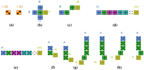
QCA cell has a quantum dot, with a four number. The shape of quantum-dot is circular with a specified diameter of 10 nm, and each dot is situated with a neighbor radius of 20 nm. Whether two extra electrons are situated in existing two quantum dots, and the arrangement is always in a diagonal way (Sen, Dutta, Some, & Sikdar, Citation2014). The formed QCA cell can be definite polarization as shown in Figure (a). Polarization can set the binary value stored in QCA cells.
Figure 1. QCA basics (a) Polarization, (b) MV, (c) inverter, (d) binary wire, (e) Inverter chain, (f) even number of rotated cells, (g) odd number of rotated cells and (h) various structures.
2.2. QCA logic gates
The basic logic gates in QCA such as majority and inverter gate as shown in Figure (b). The majority voter (MV) is represented as Y = AB + BC + AC, where Y is the majority of the inputs A, B, and C. Basic logic gate such as AND and OR gates can be realized with the MV by setting an input to zero and one, respectively. In the inverter 45° displacements in the two lines of the merging cells produce the complement of the input signals as shown in Figure (c). The binary wire and inverter chain are the two types of wires used for signal transfer in QCA (in Figure (d) and (e)).
2.3. QCA cell placing
The connection of a rotated cell with no rotated cell is shown in Figure (f) and (g). In both the figures, input A is transferred from a rotated cell to no rotated cell. If an even number of rotated cells is present between the input and output, then the complementary value of the input will pass to the output (In Figure (f)). If an odd number of rotated cells are present between the input and output, then the actual value of the input will pass to the output as shown in Figure (g). Similarly, other QCA structures are shown in Figure (h), depicting different configurations of binary wires and inverter chains.
2.4. QCA clocking
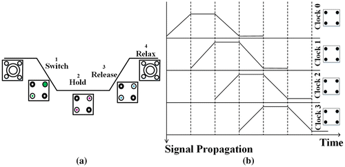
In a CMOS-based system, timing is controlled by a reference signal (i.e., a clock) and is mostly required for sequential circuits. However, timing in QCA is necessary for both combinational and sequential circuits and is accomplished by clocking in four distinct periodic phases (Hennessy & Lent, Citation2001). Clocking provides power gain in QCA (Lent & Isaksen, Citation2003) as well as the control of the information flow between the cells.
The clocking scheme in QCA consists of four phases (Hennessy & Lent, Citation2001): Switch, Hold, Release and Relax, as shown in Figure (a). QCA circuit has different partitions called clocking zones. All cells in a zone are controlled by the same clock signal. In the Relax phase, the cell is in the null state. During the switch phase, the cell attains a definite polarity under the influence of its neighbors (which are in the hold phase). In the hold phase, a cell retains its polarity and acts as the input to the neighboring cells. Finally, in the release phase, the cell loses its polarity. The clocking zones in a QCA circuit are arranged periodically. All cells within the same zone are allowed to switch simultaneously, while the cells in different zones are isolated. Consider the binary wire as shown in Figure (b); initially, clock 0 cell is in the switch phase, and clock 1 cell has no definite polarization. Then, clock 0 cell enters the hold phase, and simultaneously, clock 1 cell starts switching. Here, clock 2 cell will not influence the polarization state of clock 1 cell, because it is in the relaxed state. Then, clock 0 cell is moved to the Release phase, while clock 1 cell is in the hold state and serves as an input to the clock 2 cell, which is in the switch phase. Thus, a binary wire propagates the signal in the different clock zones.
Figure 2. QCA Clocking scheme (a) clocking phases and (b) switching of a binary wire.
3. Review of previous work
Currently, the design of logic gates in QCA is a preferred research area for building efficient QCA devices. These logic gates can be categorized into mainly two types: reversible and parity-preserving. Reversible gates have the advantage of low power dissipation; whereas, parity-preserving gates have the advantage of fault-tolerance (Parhami, Citation2006). Several QCA reversible gates such as the Feynman (Toffoli, Citation1980), QCA1 (Ma, Huang, Metra, & Lombardi, Citation2008), RUG (Sen, Saran, Saha, & Sikdar, Citation2011), TR (Das & De, Citation2016a), RM (Sen, Dutta, Goswami, & Sikdar, Citation2014), RQCA (Sen et al., Citation2014), and a reversible gate (Chabi et al., Citation2016) are mentioned in the literature. Similarly, several parity-preserving gates such as the CQCA (Thapliyal & Ranganathan, Citation2009), MX-QCA (Thapliyal, Ranganathan, & Kotiyal, Citation2013), t-QCA (Sen, Dutta, & Sikdar, Citation2014), TPC-QCA (Karkaj & Heikalabad, Citation2016), and the t-Adder (Goswami, Sen, Mukherjee, & Sikdar, Citation2017) are reported in QCA. Previously, only three logic gates, i.e., the Fredkin (Fredkin & Toffoli, Citation1982) and the parity- preserving reversible QCA gate (PPRG) (Roohi, Zand, Angizi, & Demara, Citation2016) and R-CQCA (Misra et al., Citation2017) had reported both a reversible logic and parity-preserving capability. All these gates are 3 × 3 (three inputs and three outputs) in size, except the Feynman gate, which is 2 × 2 and the R-CQCA, which is 4 × 4. The Fredkin gate is a universal gate; however, it is difficult to construct large circuits with this gate (Sen et al., Citation2014; Thapliyal et al., Citation2013). The PPRG gate is capable of self-checking active fault recovery using a cascaded arrangement (Roohi et al., Citation2016), but the disadvantage is that it requires a large number of QCA cells.
Lots of works are available on synthesizing reversible parity generator, parity checker and D latch. Some literature reviews on these testable circuits are given as Das and De (Citation2016b) proposed a reversible parity generator and parity checker followed by the QCA implementation. A reduced set of QCA primitives was performed on designs. The cell count of 72, area of 0.078 μm2 and six majority gate was reported for reversible odd parity generator. Reversible odd parity checker correctly classified cell count of 130, area of 0.143 μm2, and nine majority voter gates. The limitation of these designs is the more cell count involved in the QCA architecture. In this work, we compared the primitives results based on QCA paradigm were reported (Das & De, Citation2016b). Recently, a lot of D latch are implemented in reversible logic based (Hari, Shroff, Mahammad, & Kamakoti, Citation2006; Misra et al., Citation2017; Thapliyal et al., Citation2013). Misra et al. (Citation2017) proposed D latch approach for logic synthesis and R-CQCA and F2G gates be utilized to reduce the garbage output and make representation more compact. Here the quantum cost of D latch is tremendously reduced. The design has quantum schematics and synthesizes output. Since most of the testable reversible circuits utilize gate architecture, this work is valuable in understanding the logic computation behavior of this QCA paradigm.
4. New parity-preserving reversible gate in QCA
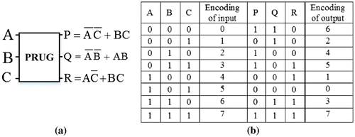
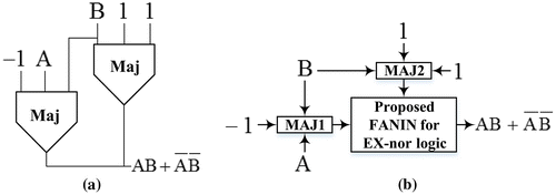
A 3x3 parity preserving reversible universal gate (PRUG) is proposed in herewith and is drawn in Figure (a). It has three- inputs and outputs; the input-output mapping is, P = A′C′ + BC, Q = A′B′ + AB, and R = AC′ + BC. The proposed PRUG gate is realized to be Ex-NOR gate by the second output Q. The reversible truth table of PRUG is presented in Figure (b). The truth table of the proposed PRUG gate confirms that it is a reversible gate with a parity-preserving capability satisfying the following two conditions:
| (1) | One-to-one mapping between the inputs and outputs. | ||||
| (2) | XOR of the inputs produces a result equal to the XOR of the outputs (A⊕ B⊕ C = P⊕ Q⊕ R). | ||||
Figure 3. Parity-preserving reversible PRUG (a) schematic and (b) truth table.
The proposed PRUG gate is a universal gate which can synthesize 13 standard Boolean functions as shown in Figure . Table provides 13 standard Boolean functions on the gate count comparison of several existing gates.
Figure 4. Implementation of the thirteen standard functions.
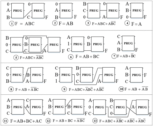
Table 1. Performance of the PRUG in realizing the standard functions with existing parity-preserving reversible gates
4.1. Proposed gate implementation
The schematic implementation of Figure (a) for QCA framework is given in Figure (b). The value of output expression plays a role in framing the QCA layout because it is part of the design. However, it is noted that a large number of logic gates in output expression requires the large cell count of the layout, which can increase the latency and area of the design. To verify the circuit workability, QCADesigner is utilized to simulate the proposed circuits, using a bistable-approximation engine and some standard QCA dimension (Walus et al., Citation2004) as shown in Figure . In this work, the Ex-NOR design is chosen to optimize the layout. Figure (a) show the proposed Ex-NOR design in QCA. The proposed Ex-NOR design is found to be 14 cells and area of 0.02 μm2. This layout is a modification of the Ex-OR QCA layout proposed in Chabi et al. (Citation2016).
Figure 5. The standard QCA cell dimensions.
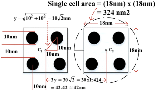
Figure 6. QCA layout of an (a) Ex-NOR gate, (b) PRUG gate and (c) simulation result.
The proposed PRUG layout is based on the configuration presented in Figure (b). As seen, the layout consists of the 109 cell count, 0.11 μm2 area, and one latency. As seen in the layout of PRUG that proposed Ex-NOR layout is utilized to robust the design. Also, coplanar crossing technique also plays roles in robust. The robust was evaluated using cell count, area, latency, and clock utilized. Figure (c) shows the simulation result which is required one latency for three outputs. Proposed layout of PRUG also compares the performance results with some of other existing reversible gates layout as shown in Table . It indicates there is an improvement of 36% in Cell count and 42% in the area compared to previous best design (Roohi et al., Citation2016).
Table 2. Comparison of the proposed gate with existing gates
5. Energy dissipation evaluation
Two type of energy dissipation, leakage energy and switching energy dissipation, for the QCA layout. To estimate the energy dissipation, the layout of the design is evaluated by using the QCAPro tool at the three different tunneling energy (0.5, 1.0 and 1.5 Ek) (Srivastava, Asthana, Bhanja, & Sarkar, Citation2011). Figure shows the thermal layout (Power dissipation map) of PRUG gate. The comparison of energy dissipation between the proposed PRUG layout and existing parity-preserving reversible gates layout are shown in Table . The energy evaluation shows that the total energy dissipation in the proposed PRUG is decreased by 48.72, 46.15, and 35.85% compared with the FRG, R-QCA and PPRG gates respectively at 0.5 Ek kink energy. Hence the proposed PRUG gate achieves energy saving ability with a smaller footprint area compared to existing gates. Finally, it can be said that proposed PRUG give lower QCA primitives, minimal energy dissipation evaluation and it is better as far as QCA computing application.
Figure 7. Power dissipation map of the PRUG.
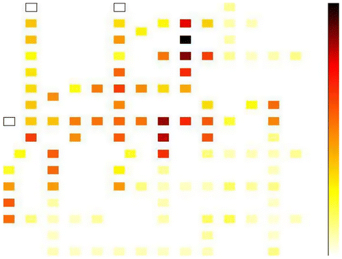
Table 3. Energy dissipation results of parity-preserving reversible gates
6. Fault-tolerance analysis of PRUG
In this section, the fault-tolerance analysis of the PRUG gate is performed. Synthesis and deposition are two phases during the manufacturing of QCA devices during which the QCA cells are susceptible to missing and additional cell defects (Momenzadeh, Ottavi, & Lombardi, Citation2005). If a particular cell is missing, it is known a missing cell defect, and if an additional cell is deposited on the substrate, it is an additional cell defect. In this work, the fault-tolerant attribute of the proposed PRUG gate is validated for these two types of defects. This validation is done by converting our proposed PRUG layout into corresponding hardware language notations using the HDLQ Verilog library (Ottavi, Schiano, Lombardi, & Tougaw, Citation2006). The HDLQ design tool has a library of QCA devices including the majority voter (MV), inverter (INV), fan-out (FO), cross wire (CW), and the L-shape wire (LS). All these devices have fault injection capabilities for validating the fault-tolerance capability of any QCA device.
Proposed Ex-NOR gate QCA schematic is shown in Figure (a). If multiple lines are connected to a single line, then this single line has a fan-in on its inputs. In the proposed Ex-NOR gate QCA schematic, there is a fan-in on the final output line; however, in the HDLQ library, there is no model available for fan-in inputs. Here, we have proposed an HDLQ model for the fan-in of the Ex-NOR gate, as depicted in Figure (b). In the proposed model, we have considered only the missing cell defects. If a missing cell fault occurs in the output of majority voter1 (MAJ1) line, then the output will be one. Similarly, if a missing cell fault occurs in the output line of majority voter2 (MAJ2), then the output will be AB. If there are no missing cell faults in both the lines, then, the output will be AB + A′B′. Herein, the following Verilog language notation-based pseudocodes describe the property of all the HDLQ model components, including our proposed fan-in for the Ex-NOR gate; fault_1 and fault_2 are the two probable faults in the pseudocodes.
Figure 8. Proposed Ex-NOR gate (a) QCA block diagram and (b) HDLQ model.
1: Crosswire
input: input1, input2, fault_1, fault_2
output: output1, output2
output1 = fault_1 ? (~fault_2 ? ~input1: input1): input1;
output2 = fault_2 ? (~fault_1 ? ~input1: input2) : input2;
2: Fanout
input: input1, fault_1
output: output1,output2
output1 = input1;
output2 = fault_1 ? ~input1: input1;
3: Inverter
input: input1, fault_1
outout: output1
out = fault_1 ? input1 : ~input1
4: Lshape wire
input: input1, fault_1
output: output1
output1 = fault_1 ? ~input1: input
5: Majority voter
input: A, B, C, fault_1, fault_2
output: output1
wire: wire1, wire2, wire3
wire1 = (A&B) | (B&C) | (A&C)
wire3 = (~A & B) | (B & ~C) | (~A & ~C)
wire2 = (fault_2) ? B: wire1
output1 = (fault_1) ? wire3 : wire2
6: Proposed Fan-in
input: A, B, fault_1, fault_2
output: output1
wire: wire1, wire2;
wire1 = (A & B) | (~A & ~B)
wire2 = (fault_2) ? B: wire1
output1=(fault_1) ? A: wire2
The HDLQ model design for the proposed PRUG gate is shown in Figure . The model contains 28 elements (MV = 7, INV = 4, LS = 6, CW = 3, FO = 7, Fan-in = 1). Exhaustive testing is conducted for this model using eight input test vectors in the presence of all the possible missing/additional cell defects in the MV, INV, CW, FO, LS, and the proposed fan-in. The design is simulated using a Verilog HDL simulator that generates a total of 39 fault-patterns. Each MV, CW, and proposed fan-in generate two fault-patterns, whereas, each INV, FO, and LS generate one fault-pattern. Out of the 39 fault-patterns, 29 are unique, as shown in Table . This table is divided into two parts: the first part depicts fault-patterns 1–15 and the second, fault-patterns 16–29.
Figure 9. HDLQ model of the proposed PRUG gate.
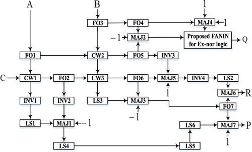
Table 4. Fault-patterns in the PRUG gate
In the fault-patterns shown in Table , ai is a three-bit pattern with an equivalent decimal value, i. For example, a0 significant that 000 (decimal 0) and a7 represents 111 (decimal 7). In Table , the first two columns depict the input test vectors and fault-free test vectors. Each row of Table represents the outputs generated after fault injection in the 39 different modules of the HDLQ model (Figure ). From these fault-patterns, we observed that there is an average of 42.37% successful patterns that generates the true output, even when there is a fault.
7. Online testing of the PRUG-based circuit
In parity-preserving logic gates, the input and output parities are the same. Hence, any single line fault in the gate can be easily tested by comparing the parity. Here, we propose three-bit novel reversible even parity generator and four-bit reversible even parity checker circuits for online fault detection in the PRUG gate. Parity generator is the operation that Ex-OR of an inputs bits. Implementation of parity checker operation can be required parity generator and inputs bits, which is especially suitable for testability. To facilitate this design, we present a novel XOR gate, which is used for designing the reversible Feynman gate. Eventually, this gate is used for designing reversible even parity generator and checker circuits. All the circuits are synthesized and simulated with QCADesigner (Walus et al., Citation2004). The designs kept in mind is that for a properly chosen layout structure, no known crossover can be used to increase the delay through the task of the robust structure.
7.1. The proposed Ex-XOR design in QCA
Here, we present a new two input Ex-OR gate in QCA framework. Figure (a) shows the block diagram and layout of the 2-input Ex-OR gate. The simulation result satisfies the functionality with a 0.5 clock delay as shown in Figure (b). The QCA primitives results of proposed Ex-OR layout is verified from Table that Cell count of 11, the area of 0.02 μm2 and latency of 0.5. Hence, it can be proof this proposed Ex-OR layout is robust and minimum Cell count, area and latency as compare to existing layouts (Angizi, Alkaldy, Bagherzadeh, & Navi, Citation2014; Karkaj & Heikalabad, Citation2017; Sasamal, Singh, & Ghanekar, Citation2016; Singh, Sarin, & Raj, Citation2016). The significant advantage is that it requires only one majority voter and one inverter, which is highly efficient for designing complex QCA circuits.
Figure 10. Exclusive-OR gate (a) block diagram and QCA layout (b) simulation result.
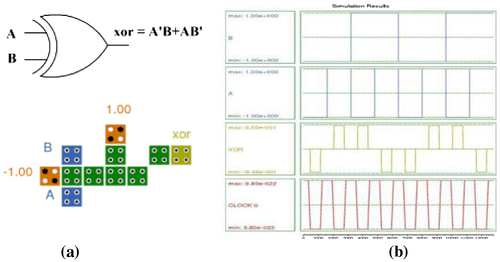
Table 5. Comparison of the 2-input XOR gates in QCA
7.2. Feynman gate implementation
The Feynman gate (FG) is also called a CNOT gate. It is a 2 × 2 reversible gate, where the inputs A and B, are mapped to the outputs P and Q, as P = A and Q = (A⊕ B) (Das & De, Citation2016a; Citation2016b). Here, the Feynman gate is designed using our proposed Ex-OR gate. It requires only 13 cells with a 0.5 clock delay. The block diagram and layout of this gate are depicted in Figure (a) and (b) respectively. Comparisons with the existing FG layout and proposed FG layout are shown in Table . It is shown that there is an improvement of 64.86 and 33% in Cell count and latency respectively.
Figure 11. Feynman gate (a) block diagram and (b) QCA layout.
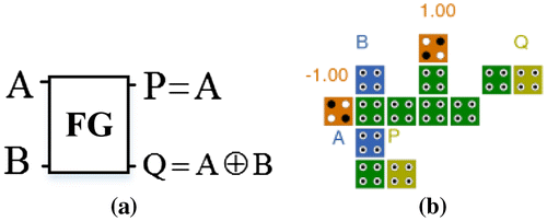
Table 6. Comparison result of Feynman gates in QCA
7.3. Proposed reversible even parity generator and checker
In this section, new even parity generator and even parity checker circuits are designed in QCA. The proposed FG is employed in these circuits construction. The QCA implementation of FG is depicted in Figure (a). The block diagram and QCA layout of the reversible even parity generator are shown in Figure (b). The QCA layout of the three-bit parity generator has 27 cell count with an area of 0.06 μm2. The block diagram and QCA layout of the reversible 4-bit even parity checker are shown in Figure (c). In this circuit, the parity check bit is equal to (P⊕ Q⊕ R⊕ Parity-bit). This layout requires 42 cell Cell count with an area of 0.10 μm2. Table reports the comparison of the proposed parity generator and checker circuits with the existing circuits.
Figure 12. Proposed QCA design of (a) FG, (b) Even parity generator and (c) Even parity checker.
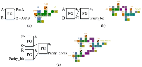
Table 7. Comparison statistics of parity generator and checker
In Table , it is reported that proposed even parity generator and even parity checker circuits very less number of majority voters and inverters compared to previous design. Therefore, there is an improvement in cell count of 62% for even parity generator and 67% for even parity checker.
7.4. Proposed structure of the online fault detection based on proposed gate
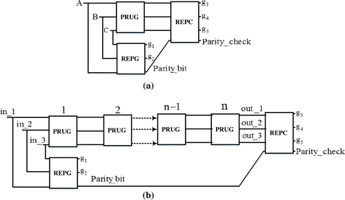
Parity generator circuits generate a bit by considering the number of 1’s in the inputs. If the number of 1’s in the input are even, then the even parity generator generates a zero. Otherwise, it generates a one. This generated parity bit is transferred to the outputs. Parity checker circuits take the generated parity bit and perform an Ex-OR operation with the output bits of the PRUG to generate the parity check bit. If the parity check bit is zero, the PRUG is fault-free. Otherwise, it is faulty. The structure of the online testable PRUG gate with even parity generator and even parity checker circuits is shown in Figure (a). Here, REPG indicates a reversible even parity generator and REPC, a reversible even parity checker. The online fault detection of a completely cascaded arrangement of PRUG-based circuits is depicted in Figure (b). In this design, the parity generator and parity checker circuits are needed only in the first and last stages, respectively. In a partially-cascaded arrangement, constant inputs are provided to the PRUG gates. Therefore, in this arrangement, the parity generator and parity checker circuits are needed at each stage, where constant inputs are provided to facilitate online fault detection.
Figure 13. Proposed online testable circuits (a) single PRUG gate and (b) cascaded arrangement of PRUG gate-based circuits.
8. Proposed D latch based on proposed gate
The D latch is the basic memory element for all the sequential devices. The Boolean equation for a positive D latch is and for a negative D latch it is
, where E is the enable input. This two-to-one sized multiplexer-based Boolean equation approach exists only for the Fredkin, R-CQCA and PRUG gates in parity-preserving reversible category. Hence, our proposed gate can be a basic gate for all fault-tolerant reversible sequential devices because of optimized design in cell count, area and delay compared to others. In this work, a negative D latch is designed using a PRUG gate, as shown in Figure (a). The QCA layout and simulation results are presented in Figure (b) and (c), respectively. The drawback of the PPRG gate in designing a D latch is that two gates are required to implement the output expression of the D latch. Therefore, our proposed gate is efficient in designing a basic memory element. Similarly, a positive edge-triggered D flip-flop can be designed by cascading a negative D latch with a positive D latch. Comparison results carried out on D latch reveals that the new framework surpass the state-of-the-art designs and demonstrate promising feature of QCA computing such as cell count, area and latency, as shown in Table .
Figure 14. Parity-preserving, reversible D-latch using the PRUG gate (a) block diagram, (b) QCA layout and (c) simulation result.
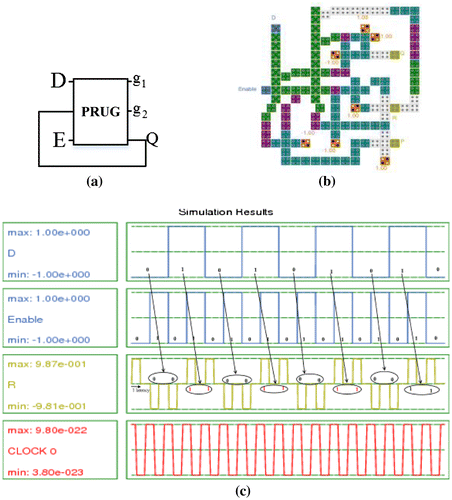
Table 8. Implementing a D-latch with a parity-preserving reversible gate
9. Conclusion
In this paper, a new parity preserving based reversible gate is designed using QCA. Our proposed logic gate is better than the existing parity-preserving reversible gates because it has achieved a 36% improvement in the cell count and a 42% improvement in the total area compared to the previous best design. We implemented all the 13 standard combinational logic functions at minimal costs. The use of single PRUG to the realization of D latch. The proposed D latch has been utilized one clock cycle delay for logic computation. Simulation results show that in D latch based QCA architecture latency is 50% improvement, and the area is 63.15% improvement than previous best parity-preserving reversible gate QCA layout which is very small and interesting. Further, we showed that Feynman gate in QCA and 64.86, 13.04, and 33.33% improvement in cell count, area, and latency respectively than the previous work. The proposed new gate and testable circuits can be helpful for designing fault-tolerant and low-power digital circuits using QCA technology.
Funding
The authors received no direct funding for this research.
Acknowledgment
The author acknowledges the Veer Surendra Sai University of Technology (VSSUT), Burla, for their financial support to carry out this research under the Technical Education Quality Improvement Programme (TEQIP-II) grant.
Additional information
Notes on contributors
Bandan Bhoi
Bandan Bhoi received the BTech in ECE from Biju Patnaik University of Technology, India in 2007 and MTech degree from IIIT Hyderabad, India in 2010. He worked as a design engineer in VLSI industry from 2010 to 2011. Currently pursuing PhD at Veer Surendra Sai University of Technology India. He is working as an assistant professor in ECE at Veer Surendra Sai University of Technology India. His research area includes Reversible Computation, QCA, and Reconfigurable computing architecture.
Neeraj Kumar Misra
Neeraj Kumar Misra is an assistant Professor of ECE department at the School of Management Science, Lucknow, India. He has completed PhD from AKTU Lucknow, India under TEQIP-II. His research includes reversible logic, and fault-tolerant digital design.
Manoranjan Pradhan
Manoranjan Pradhan received the PhD from Sambalpur University India. He is currently an assistant professor at Veer Surendra Sai University Of Technology, India. His research interests include on cryptography, and Quantum computing.
References
- Angizi, S., Alkaldy, E., Bagherzadeh, N., & Navi, K. (2014). Novel robust single layer wire crossing approach for exclusive OR sum of products logic design with quantum-dot cellular automata. Journal of Low Power Electronics, 10(2), 259–271.10.1166/jolpe.2014.1320
- Bennett, C. H. (1973). Logical reversibility of computation. IBM Journal of Research and Development, 17(6), 525–532.10.1147/rd.176.0525
- Chabi, A. M., Roohi, A., Khademolhosseini, H., Sheikhfaal, S., Angizi, S., Navi, K., & DeMara, R. F. (2016). Towards ultra-efficient QCA reversible circuits. Microprocessors and Microsystems, 49, 127–138.
- Das, J. C., & De, D. (2016a). Reversible comparator design using quantum dot-cellular automata. IETE Journal of Research, 62(3), 323–330.10.1080/03772063.2015.1088407
- Das, J. C., & De, D. (2016b). Quantum-dot cellular automata based reversible low power parity generator and parity checker design for nanocommunication. Frontiers of Information Technology & Electronic Engineering, 17(3), 224–236.
- Fredkin, E., & Toffoli, T. (1982). Conservative logic. International Journal of Theoretical Physics, 21(3), 219–253.10.1007/BF01857727
- Goswami, M., Sen, B., Mukherjee, R., & Sikdar, B. K. (2017). Design of testable adder in quantum-dot cellular automata with fault secure logic. Microelectronics Journal, 60, 1–12.10.1016/j.mejo.2016.11.008
- Hari, S. K. S., Shroff, S., Mahammad, S. N., & Kamakoti, V. (2006). Efficient building blocks for reversible sequential circuit design. Circuits and Systems, 2006. MWSCAS’06. 49th IEEE International Midwest Symposium on (Vol. 1). IEEE.
- Hennessy, K., & Lent, C. S. (2001). Clocking of molecular quantum-dot cellular automata. Journal of Vacuum Science & Technology B: Microelectronics and Nanometer Structures Processing, Measurement, and Phenomena, 19(5), 1752–1755.10.1116/1.1394729
- Karkaj, E. T., & Heikalabad, S. R. (2016). A testable parity parity-preserving gate in quantum-dot cellular automata. Superlattices and Microstructures.
- Karkaj, E. T., & Heikalabad, S. R. (2017). Binary to gray and gray to binary converter in quantum-dot cellular automata. Optik-International Journal for Light and Electron Optics, 130, 981–989.10.1016/j.ijleo.2016.11.087
- Landauer, R. (1961). Irreversibility and heat generation in the computing process. IBM Journal of Research and Development, 5(3), 183–191.10.1147/rd.53.0183
- Lent, C. S., & Isaksen, B. (2003). Clocked molecular quantum-dot cellular automata. IEEE Transactions on Electron Devices, 50(9), 1890–1896.10.1109/TED.2003.815857
- Ma, X., Huang, J., Metra, C., & Lombardi, F. (2008). Reversible gates and testability of one dimensional arrays of molecular QCA. Journal of Electronic Testing, 24(1–3), 297–311.10.1007/s10836-007-5042-2
- Misra, N. K., Sen, B., & Wairya, S. (2017). Towards designing efficient reversible binary code converters and a dual-rail checker for emerging nanocircuits. Journal of Computational Electronics, 16(2), 442–458.10.1007/s10825-017-0960-4
- Misra, N. K., Wairya, S., & Sen, B. (2017). Design of parity-preserving, reversible sequential logic for cost efficient emerging nano circuits with enhanced testability. Ain Shams Engineering Journal.
- Momenzadeh, M., Ottavi, M., & Lombardi, F. (2005). Modeling QCA defects at molecular-level in combinational circuits. Defect and Fault Tolerance in VLSI Systems, 2005. DFT 2005. 20th IEEE International Symposium on. IEEE.
- Ottavi, M., Schiano, L., Lombardi, F., & Tougaw, D. (2006). HDLQ: A HDL environment for QCA design. ACM Journal on Emerging Technologies in Computing Systems (JETC), 2(4), 243–261.10.1145/1216396
- Parhami, B. (2006). Fault-tolerant reversible circuits. Signals, Systems and Computers, 2006. ACSSC’06. Fortieth Asilomar Conference on. IEEE.
- Roohi, A., Zand, R., Angizi, S., & Demara, R. F. (2016). A parity-preserving reversible QCA gate with self-checking cascadable resiliency. IEEE Transactions on Emerging Topics in Computing, 1, 1–1.10.1109/TETC.2016.2593634
- Sasamal, T. N., Singh, A. K., & Ghanekar, U. (2016). Design of non-restoring binary array divider in majority logic-based QCA. Electronics Letters, 52(24), 2001–2003.10.1049/el.2016.3188
- Sen, B., Dutta, M., Goswami, M., & Sikdar, B. K. (2014). Modular design of testable reversible ALU by QCA multiplexer with increase in programmability. Microelectronics Journal, 45(11), 1522–1532.10.1016/j.mejo.2014.08.012
- Sen, B., Dutta, M., & Sikdar, B. K. (2014). Efficient design of parity preserving logic in quantum-dot cellular automata targeting enhanced scalability in testing. Microelectronics Journal, 45(2), 239–248.10.1016/j.mejo.2013.11.008
- Sen, B., Dutta, M., Some, S., & Sikdar, B. K. (2014). Realizing reversible computing in QCA framework resulting in efficient design of testable ALU. ACM Journal on Emerging Technologies in Computing Systems (JETC), 11(3), 30.
- Sen, B., Saran, D., Saha, M., & Sikdar, B. K. (2011). Synthesis of reversible universal logic around QCA with online testability. In Electronic System Design (ISED), 2011 International Symposium on. IEEE
- Singh, G., Sarin, R. K., & Raj, B. (2016). A novel robust exclusive-OR function implementation in QCA nanotechnology with energy dissipation analysis. Journal of Computational Electronics, 15(2), 455–465.10.1007/s10825-016-0804-7
- Srivastava, S., Asthana, A., Bhanja, S., & Sarkar, S. (2011). QCAPro-an error-power estimation tool for QCA circuit design. Circuits and Systems (ISCAS), 2011 IEEE International Symposium on. IEEE.
- Thapliyal, H., & Ranganathan, N. (2009). Parity-preserving QCA gate (CQCA) for designing concurrently testable molecular QCA circuits. VLSI Design, 2009 22nd International Conference on. IEEE.
- Thapliyal, H., Ranganathan, N., & Kotiyal, S. (2013). Design of testable reversible sequential circuits. IEEE Transactions on Very Large Scale Integration (VLSI) Systems, 21(7), 1201–1209.10.1109/TVLSI.2012.2209688
- Toffoli, T. (1980). Reversible computing. Automata, Languages and Programming, 632–644.
- Walus, K., Dysart, T. J., Jullien, G. A., & Budiman, R. A. (2004). QCADesigner: A rapid design and simulation tool for quantum-dot cellular automata. IEEE Transactions on Nanotechnology, 3(1), 26–31.10.1109/TNANO.2003.820815
- Zhang, R., Walus, K., Wang, W., & Jullien, G. A. (2004). A method of majority logic reduction for quantum cellular automata. IEEE Transactions on Nanotechnology, 3(4), 443–450.10.1109/TNANO.2004.834177