
Abstract
Thin films of CuGaSe were deposited on n-Si (1 0 0) by rf magnetron sputtering from a stoichiometric CuGaSe2 target. The objective of this study was to characterize the thin film/Si heterojunction for potential photovoltaic applications, evaluate possible candidates for metal contacts and to establish whether heteroepitaxial growth could be achieved, particularly as the mismatch of lattice parameters corresponding to the base of the copper gallium selenide (CGS) tetragonal cell is quite close to that of Si, with a 2.9% mismatch. For this study, Si substrates were prepared by the standard Radio Corporation of America (RCA) cleaning procedure immediately followed by the deposition of CGS by sputtering at a substrate temperature of 600°C. The deposited thin-film stoichiometry and morphology were characterized by Rutherford backscattering spectroscopy (RBS) and transmission electron microscopy (TEM). Rutherford back scattering (RBS) analysis indicated a thin-film composition of Cu1Ga1Se1 indicating that the films were Se deficient, although channeling was not observed. The polycrystalline nature of the deposited thin film was established by cross-sectional TEM. An estimated 1.5-nm thick layer likely to be SiO x was observed at the CGS–Si interface. It is believed that this interfacial layer prevented heteroepitaxy CGS on Si. Additionally, circular metal contacts were deposited on the thin films and characterized by capacitance and current–voltage measurements. It was observed that Al and Ag contacts were rectifying, from which the thin-film carrier density was estimated to be ~5 × 10¹⁵ and ~7.68 × 1015 cm−3 with Al and Ag contacts, respectively. Au, Pt, W and Cr were ohmic, and Mo and Ni provided semi-ohmic contacts to CGS films.
PUBLIC INTEREST STATEMENT
Renewable energy resources have enormous potential and can meet the present world energy demand. Among the different thin-film technologies, the family of chalcopyrite has demonstrated high efficiency and low cost for solar cells. A large number of chalcopyrites exhibit direct bandgaps and relatively narrow luminescent bands (sometimes at low temperatures only) making them an interesting candidate to obtain stimulated emission/laser action. Thin-film copper indium–gallium selenide solar cells have exceeded 20% efficiency. Thus, the efficiency is the important factor which needs to be explored further for the best implementation and utilization of emerging and useful technology. This paper presents a review of the growth of copper gallium selenide on Si substrate, analysis of the crystal composition and investigation of different metals for good contact formation. Further research to understand material properties of the respective components and the interface behaviors is of great importance.
1. Introduction
Thin-film CuInGaSe2 (copper indium–gallium selenide [CIGS]) has received a lot of attention, for its use as an absorber layer for thin-film solar cells (Chen et al., Citation2012; Eid, Liang, Gereige, Lee, and Van Duren, Citation2015; Hollars, Dorn, Paulson, Titus, and Zubeck, Citation2005; Hibberd et al., Citation2010; Metzner et al., Citation2002; Powalla et al., Citation2013; Rocket & Birkmire, Citation1991; Salome et al., Citation2015; Siebentritt, Citation2002; Siebentritt et al. Citation2005; Swiss Federal Laboratories for Materials Science and Technology (EMPA), www.empa.ch, press release, Citation2013; You, Hong, Jeong, and Youn Citation2008). The use of the chalcopyrite material system is attractive and important for the fabrication of thin-film solar cell using inexpensive substrates like glass (CitationLuque & Hegedus). The high absorption coefficient, radiation hardness and apparent immunity from grain boundary defects make CIGS a promising thin-film solar material. CIGS is essentially an alloy of CuInSe2 (CIS) and CuGaSe2 (copper gallium selenide [CGS]) with an optimized In-to-Ga ratio (Rocket & Birkmire, Citation1991; Siebentritt et al., Citation2005).
Individually, CIS has been extensively studied, although this material has a non-ideal bandgap of about 1 eV; CGS on the other hand with a bandgap of 1.7 eV is considered to be better suited as a solar cell material; however, the theoretically predicted conversion efficiency has not been achieved due to problems associated with this material system (Rocket & Birkmire, Citation1991; Siebentritt, Citation2002). Tuning the bandgap by addition of Ga to obtain a composition of CuIn1 − x Ga x Se2 with [Ga]/[Ga + In] ratio of 25–30% has led to a convenient fabrication process yielding a record conversion efficiency of 22.9% (Green et al., Citation2018; Powalla et al., Citation2013; Swiss Federal Laboratories for Materials Science and Technology (EMPA), Citation2013). This material system has a bandgap of about 1.2 eV, whereas the optimum bandgap for terrestrial solar cells is 1.5 eV. Solar cells employing CuIn1 − x Ga x Se2 are normally produced by depositing thin films of the material on molybdenum (Mo)-coated soda lime glass substrates (Bosio, Menossi, Romeo, & Romeo, Citation2013). Various deposition techniques including metalorganic vapor phase epitaxy, one-stage/three-stage coevaporation, cosputtering of Cu(In,Ga) followed by selenization, reactive and non-reactive sputter deposition and electrodeposition have been reported (Chen et al., Citation2012; Eid et al., Citation2015; Hibberd et al., Citation2010; Hollars et al., Citation2005; Powalla et al., Citation2013; Salome et al., Citation2015; Siebentritt et al., Citation2005; You et al., Citation2008). Typically, a thin film of CdS is deposited in a bath to form a heterojunction with CIGS (CitationLuque and Hegedus; Bosio et al., Citation2013), followed by a transparent conductor and metal contacts fabricated to complete the cell structure (Bosio et al., Citation2013).
Films of CIGS on soda Mo-coated glass substrates are polycrystalline in nature with large grains. Previously, heteroepitaxial growth of Cu(In,Ga)Se2 on Si by molecular beam epitaxy has been achieved by Metzner et al. (Citation2002).
The present study is an effort to establish whether heteroepitaxial growth of CGS/CIGS on Si substrates could be achieved Radio Frequency (RF) magnetron sputtering and to investigate the characteristics of the contact formed between the thin film and potential metal top contacts. The rational for employing a Si substrate is that there is a close match of 2.9% between the lattice parameters corresponding to the base of the CGS tetragonal cell (a = 0.559 nm) and that of Si unit cell, whereas the mismatch for CIS (a = 0.5798 nm)/Si is 6.8%. Considering the small mismatch for CGS, heteroepitaxy may be achieved on an atomically clean Si (1 0 0) surface if the right deposition conditions could be established. Following the initial deposition of a very thin layer of CGS or CIS, In or Ga could be introduced gradually to form a CIGS film with optimum In/Ga content. The absence of grain boundaries, although benign, in a heteroepitaxial CIGS film on Si (1 0 0) may provide a high-quality p-CIGS/n-Si photovoltaic junction. Use of commercially available thin Si substrates could be employed in order to provide a low series resistance, as Si serves as a substrate providing a heterojunction; however, the structure does not rely on the absorption of Si. The p-CGS/CIGS/n-Si may serve as a lower junction of a Si-based tandem structure with a ZnSe/ZnTe upper cell. The study reported here involves microstructural characterization of CGS films grown on (1 0 0) Si by rf magnetron sputter deposition from a stoichiometric CuGaSe2 target as well as the characterization of metal contacts as potential candidates for use in the top contact structure of the solar cell structure. Additionally, there is presently a lack of fundamental knowledge relating film characteristics to device properties and performance. We attempt to develop a fundamental and detailed understanding of the film composition, surface and interface effects that could potentially limit device performance.
2. Experiment
Silicon (1 0 0) n-type wafers diced into 1 cm × 1 cm samples were cleaned using a standard RCA cleaning procedure. Following the RCA step, the Si samples were treated in buffered oxide etch (BOE) to remove any surface oxide, then blow dried with nitrogen and immediately placed in the sputtering chamber (AJA International Orion-5). Metal and stoichiometric CuGaSe2 targets (99.99%, Plasmaterials Inc., CA) were used as the source. The distance between the substrate and target was approximately 12.5 cm. The sputtering system was pumped down to a base pressure in the range of (4.7–8.6) × 10−7 Torr. Argon was introduced into the chamber at a flow rate 10 sccm. The substrate heater was then turned on and Si samples were heated to a temperature of 600°C. In order to strike the RF plasma, the chamber pressure was raised to 25–30 mTorr. The RF power unit was initially set to 30 W and increased by 5 W/min to 50 W. The tune and load settings were adjusted to ensure that the reflected power was 0 W and plasma was eventually ignited. The chamber pressure was reduced to the processing pressure of 11 mTorr. Prior to the initiation of CGS deposition, pre-sputtering was performed for 5 min with the shutter closed over the samples in order to remove contaminants from the surface of the target. The substrate holder was rotated at a speed of 14 rpm and the shutter was opened. After a given time, the process was terminated by first closing the shutter and decreasing the power by a rate of 5 W/min to reach 20 W, and then the power was turned off. At this juncture, the Ar flow was turned off. The substrate heater was turned and allowed to cool down to 250°C and the chamber was pumped down to base pressure prior to unloading. A summary of the sputtering process is presented in Table .
Table 1. RF and dc magnetron sputtering parameters/process conditions used for Cu1Ga1Se1 and metal film depositions
The thickness of the deposited CGS and metal films was measured using a surface contact profiler (KLA Tencor p-6) and deposition rates were determined. Rutherford back scattering was used for determining the composition of the CGS films. A 2-MeV He+ beam was employed for the Rutherford backscattering spectroscopy (RBS) analysis. Samples of 1 cm2 of deposited absorber material were mounted to a target using silver paint. The He+ ion beam was accelerated toward the samples using a tandem electrostatic accelerator. Samples were bombarded with the He+ beam. The yield as well as energy distribution of the backscattered He+ ions at a given angle were measured and recorded. Transmission electron microscopy (TEM) of a cross-sectional sample was performed to study the interface between the CGS film and the Si substrate, and the nature of the deposited films. The cross-sectional sample strips were prepared from the 1-cm2 samples which were cross-sectioned and glued back to back, dimpled and then ion-milled. Diffraction patterns and high magnification images of the sample cross-sections were obtained. This analysis was used to obtain morphologic, compositional and crystallographic information on deposited absorber samples. Bright and dark field images as well as high resolution micrographs and selected area electron diffraction patterns (selected area diffraction patterns [SADPs]) were obtained.
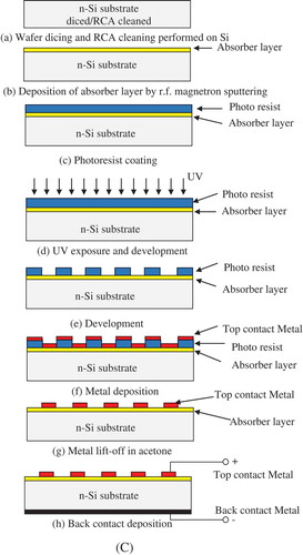
To evaluate the electrical characteristics of deposited contacts, test patterns were defined by photolithography and metal contacts were formed by dc sputter deposition and a subsequent photoresist lift-off procedure. Microposit S1813-positive photo resist was employed for pattern transfer by photolithography.
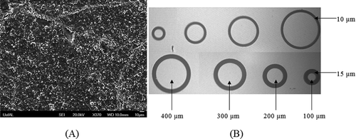
A Headway Research PWM32 spin coater was used to obtain photo resist coating on samples, employing a spin speed of 400 rpm for 5 s and 4,000 rpm for 30 s, to obtain a photo resist thickness of ~1,400 nm. The samples were then soft baked at 90°C for 60 s, and patterns were defined by photolithography using a Karl Suss MJB3 mask-aligner. A UV exposure of 12 s was applied through an appropriate mask. The exposed samples were then developed and patterns visually inspected under a microscope. Figure (A,B) shows a representative scanning electron micrograph of the CuGaSe thin-film surface (X370) and microscopic images of metal contact patterns. Deposition of metal films was performed by dc magnetron sputtering technique. Film deposition rates were studied by measuring the thickness of the deposited metal films while optimizing the process conditions. Contacts to the CGS films were formed by dc sputtering of several metals with varying work function including Ag, Al, W, Cr, Mo, Ni, Au and Pt. Metal contacts were electrically characterized in the as-deposited state and after an anneal treatment using circular contact dot patterns of varying diameter (100, 200, 300 and 400 µm diameter) (CitationSchroder). The fabrication process flow is presented in Figure (C).
Figure 1. (A) Representative SEM micrograph (plan view) of a 200-nm thick CuGaSe film deposited by RF sputtered at 600°C from a stoichiometric target (B). Microscopic image of metal contact patterns developed on a CuGaSe thin film: dots separated from infinite area contact by an annular ring space for contact type determination. (C) Si/CGS heterojunction fabrication process flow.
3. Results and discussion
3.1. Analysis of thin composition and morphology
CGS films deposited at a temperature of 600°C for 90 min yielded a thickness of ~215 nm. These films were visually semitransparent. A representative RBS spectrum obtained from the CGS samples is shown in Figure (A). Average thickness of 215 nm and a composition of Cu1Ga1Se1 were obtained from the RBS spectra using “RUMP-RBS Analysis and Simulation” software. Thin films were prepared from a stoichiometric alloy sputtering target (CuGaSe2). However, since the films were deposited in the absence of excess selenium (Se), the films turned out Se deficient as indicated by RBS. This may be due to Se loss in the vacuum chamber or insufficient Se from the target and may be compensated for by an excess Se supply, higher Se ratios in the target or post-selenization of sputtered films.
Figure 2. (A) Rutherford backscattering (RBS) spectra from CGS films grown for 90 min at a substrate temperature 600°C. Simulated profiles obtained using “RUMP-RBS Analysis and Simulation” package are shown in red. (B) Bright field transmission electron micrograph and (C) dark field cross-sectional transmission electron micrograph showing the polycrystalline nature of the CGS film. Samples of CuGaSe were deposited at a substrate temperature of 600°C for 90 min.
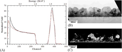
Cross-section TEM was undertaken to examine the details of one CGS-on-Si sample. Accompanying bright and dark field images are shown in Figure (B) and (C), respectively.
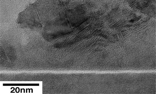
From the micrographs above, film roughness is evident as well as its polycrystalline grain structure. The film thickness was estimated to be 215 nm using RBS and TEM; this agrees well with the thickness estimates using the stylus profiler. High-resolution TEM (HRTEM) results are shown in Figure . An apparent interlayer of ~1.5 nm thickness is observed. It appears that this interlayer prevented heteroepitaxy from occurring.
Figure 3. High-resolution TEM micrograph showing the interface between the Si substrate and the CGS film.
Selected area diffraction patterns (SADPs) were taken; an example is shown in Figure . The reflections associated with the Si [0 1 1] single crystal pattern were used to establish the camera constant and which was used to evaluate the diffraction results from the film; d-spacing results are compiled in Table . We observe that many measured d-spacings are similar and close to those expected from Si. Additionally, we observe evidence of additional reflections, such as the {2 0 0} and {2 2 2}, both of which are not permitted for the diamond cubic lattice. They are, however, permitted from the zinc-blende crystal structure (e.g. GaAs). This implies that we have cation–anion ordering in the film. Interestingly, we have observable, but as of now, not fully explained reflections. These may indicate that there is additional ordering on the cation sublattice and there may be a tendency for the body-centered tetragonal chalcopyrite phase to be present to some degree. The possibility of a mixed phase film cannot, at this time, be ruled out either. At this point, it appears that the film is likely to be mainly cubic with the zinc-blende crystal structure.
Table 2. Compiled electron diffraction results
Figure 4. Selected area electron diffraction pattern of Si [0 1 1] superimposed on the polycrystalline CGS film.
![Figure 4. Selected area electron diffraction pattern of Si [0 1 1] superimposed on the polycrystalline CGS film.](/cms/asset/41441473-713f-4ffa-a0fe-3e17657cb78a/oaen_a_1514941_f0004_b.gif)
The formation of the interlayer at the CGS/Si interface can be attributed to a few factors. There is the possibility of partial oxidation due to the presence of residual amount of O2 and H2O in the sputter chamber. In this work, the pump-down process to reach the base pressure took several hours as the sputter chamber did not have a load lock. There is also the aspect of native oxide growth prior to sample placement in the sputtering chamber. Silicon substrates used for CGS deposition were treated in BOE and dried in N2, and immediately loaded into the sputter chamber. The total time of sample exposure to air was not more than a few minutes. At an ambient temperature of 25°C or less and humidity of 50% or less, this would entail the growth of a native oxide less than 0.5 nm thick before the samples were placed in the sputtering chamber.
3.2. Metal contact characterization, built-in potential and carrier concentration
3.2.1. Current–voltage measurements
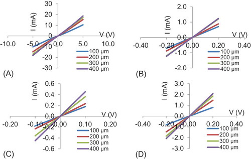
The nature of the contacts (ohmic or rectifying) was investigated by simple current–voltage (I–V) methods. Current–voltage measurements were obtained by probing samples using a Cascade Microtech RHM-06 probe station at room temperature (~25°C). The current and voltage values were acquired using a HP 4155A semiconductor parameter analyzer and an in-house LabView data logging interface. Two contact patterns were used for contact studies. Ohmic contacts were further studied using Transfer Length Method (TLM) analysis to determine the specific contact resistance. Rectifying contacts were analyzed by taking C–V measurements on circular contacts to determine the built-in potential and dopant concentration of the films. Sputter deposition of various metals, Ag, Al, W, Cr, Mo, Ni, Au and Pt, was used to form contacts on CGS. The photolithographically defined circular contact patterns (100, 200, 300 and 400 µm in diameter), surrounded by large-area metalized field regions separated by annular ring spaces, were probed by I–V measurements. It was observed that Al and Ag contacts were rectifying if Au, Pt, W and Cr were ohmic, and Mo and Ni provided semi-ohmic contacts to CGS films. The I–V characteristics of ohmic contacts to CGS films established with Cr, Au, Pt and W are shown in Figure (A–D), respectively. Characteristics of these contacts did not change significantly upon anneal at 400°C for 10 min.
Figure 5. I–V characteristics of 100, 200, 300 and 400 µm ohmic for (A) Cr contact on CGS, (B) Au contact on CGS, (C) Pt contact on CGS and (D) W contact on CGS.
3.2.2. Capacitance–voltage measurements
Rectifying contacts were analyzed by obtaining capacitance–voltage (C–V) measurements at room temperature (~25°C) using an HP4284A Precision LCR (inductance, capacitance and resistance) meter in conjunction with a RHM-06 probe station on the circular contact dots of varying diameter.
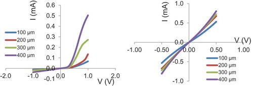
A representative plot of the rectifying and semi-ohmic characteristics produced by Ag and Mo is shown in Figure . Anneal treatments was performed on selected samples (which yielded semi-ohmic or rectifying characteristics) at temperatures between 150 and 400°C for 10–60 min, with the purpose of establishing ohmic contacts or improving the contact quality.
Figure 6. I–V characteristics of 100, 200, 300 and 400 µm: (A) rectifying Ag contacts on CGS and (B) semi-ohmic Mo contacts on CGS.
No significant improvements to the nature of the contacts were observed. Analysis of the ohmic contacts to CGS indicated a specific contact resistance of 7.9 × 10⁻⁴, 9.12 × 10⁻⁵ and 3.06 × 10⁻⁴ Ω cm2 for Au, Pt and Ni, respectively.
The capacitance was measured under reverse bias conditions at a frequency of 1 MHz and an ac signal of 20 mV rms at room temperature. Replicate thin films (N = 5) with metal contacts were prepared. From the C–V measurements, the plot of the 1/C 2 − V was used to determine built-in potential, V bi as shown in Figure (A,B). Dopant concentration was subsequently calculated. It was observed that V bi varied between 1.56 and 2.33 V for Al contact on CGS, whereas a V bi between 0.5 and 0.7 V was observed for Ag contacts on CGS with different contact sizes (diameters).
Figure 7. Capacitance–voltage measurements for rectifying Ag circular dots contacts surrounded by infinite area. (A) C–V characteristics for 400 and (B) 200 µm diameter contacts. The doping concentration and built-in potential were estimated from the slope and the intercept on the V-axis, respectively.
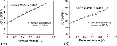
The variation in the V bi is not clearly understood but may be process related. The carrier concentrations of the CGS thin films were also calculated and were found to be in the range of ~5 × 10¹⁵ and ~7.68 × 1015 cm−3 with Al and Ag contact on CGS, respectively. A relative permittivity (ℰ r) of 6.69 and 5.02 were calculated by taking the average ℰ r obtained from the 100 to 400-µm contacts sizes for Al and Ag contact on CGS, respectively.
4. Conclusion
CGS films were deposited on n-Si (1 0 0) substrates by RF magnetron sputtering from a stoichiometric CuGaSe2 target at a substrate temperature of 600°C. Rutherford backscattering analysis yielded a random spectrum and channeling was not observed. A composition of Cu1Ga1Se1 and a thickness of 215 nm were determined from a simulation of the RBS spectrum. TEM of cross-sectional samples indicated the CGS film polycrystalline in nature with large grains. Structure of the films as determined from SADP was mixed zinc-blende structure with a tendency body-centered tetragonal phase. HRTEM micrographs indicated the presence of an approximately 1.5-nm thick layer, likely to be SiO x , at the CGS/Si interface. It is believed that the elimination of the interfacial oxide layer may permit the formation of a heteroepitaxial film. A sputtering target with substantially higher than the stoichiometric Se content is likely to yield stoichiometric CuGaSe2 and eventually high-quality Cu(In,Ga)Se2 films with the introduction of In in the sputtering target. Metal contacts were formed on CGS by sputtering. It was observed that Al and Ag contacts were rectifying, from which the thin-film carrier density was estimated to be ~5 × 10¹⁵ and ~7.68 × 1015 cm−3 with Al and Ag contacts, respectively. Au, Pt, W and Cr were ohmic, and Mo and Ni provided semi-ohmic contacts to CGS films.
Additional information
Funding
Notes on contributors
M. A. Awaah
The research team works on a number of semiconducting material systems for high speed and high efficiency device application. The groups current interests are investigating improved Si Solar Cell efficiency and Next Generation High Efficiency and low-cost Photovoltaics materials. Thin film photovoltaic materials are currently being sought as replacement to current GaAs solar arrays for space applications and as replacements for current silicon based terrestrial technology. Systems based on polycrystalline CuInGaSe2 (CIGS) absorbers have achieved efficiencies above 20%. The current research focuses on the growth and characterization of CuInSe2 (CIS), CuGaSe2 (CGS) material, and contacts studies to these films.
The authors would like to express their sincere gratitude to Drs. S. Jeelani and P. K. Ray, Tuskegee University, for their keen interest in the work and the encouragement they provided, J. Callaway for technical assistance and Tuskegee Center for Advanced Materials for providing experimental facility.
Related Research Data
References
- Bosio, A. , Menossi, D. , Romeo, A. , & Romeo, N. (2013). Polycrystalline Cu(InGa)Se2/CdS thin film solar cells made by new precursors , Edited by A. Morale-Acevedo ISBN, 978-953-51-1003-3, 386, InTech Publication under CC BY 3.0 license. Croation.
- Chen, C. H. , Shih, W. C. , Chien, C. Y. , Hsu, C. H. , Wu, Y. H. , & Lay, C. H. (2012). A promising sputtering route for one-step fabrication of chalcopyrite phase Cu(In,Ga)Se2 absorbers with extra Se supply. Solar Materials and Solar Cells , 103, 25–29. doi:10.1016/j.solmat.2012.04.008
- Eid, J. , Liang, H. , Gereige, I. , Lee, S. , & Van Duren, J. (2015). Combinational study of NaF addition in CIGSe films for high efficiency solar cells. Progress Photovolt: Researcher Applications , 23, 269–280. doi:10.1002/pip.2419
- Green, M. , Hishikawa, Y. , Dunlop, E. , Levi, D. , Hohl-Ebinger, J. , & Ho-Baillie, A. (2018). Solar cell efficiency tables (version 52. Progress in Photovoltaics: Research and Applications , 26(7), 427–436. doi:10.1002/pip.3040
- Hibberd, C. J. , Chassaing, E. , Liu, W. , Mitzi, D. B. , Lincot, D. , & Tiwari, A. N. (2010). Non-Vacuum methods for formation of Cu(In,Ga)(Se.S) 2. Progress in Photovoltaics: Research and Applications , 18, 434–452. doi:10.1002/pip.914
- Hollars, D. R. , Dorn, R. , Paulson, P. D. , Titus, J. , & Zubeck, R. (2005). Large area Cu(In,Ga)Se2 films and devices on flexible substrates made by sputtering. Materials Research Society Symposium Proceedings , 865, 477–482. doi:10.1557/PROC-865-F14.34
- Luque, A. , & Hegedus, S. (Ed.). Handbook of photovoltaic science and engineering: 2nd edition . John Wiley Inc.
- Metzner, H. , Reislohner, U. , Cieslak, L. , Witthun, W. , Hahn, T. , & Krauβlich, J. (2002). Hetero-epitaxial growth of Cu(In,Ga)S2 on Si Substrate. Thin Solid Films , 403–404, 13–16. ns, and so.
- Powalla, M. , Jackson, P. , Witte, W. , Hariskos, D. , Paetel, S. , Tschamber, C. , & Wischmann, W. (2013). High-efficiency Cu(In, Ga)Se2 cells and modules. Solar Energy Materials& Solar Cells , 119, 51–58. doi:10.1016/j.solmat.2013.05.002
- Rocket, A. , & Birkmire, R. W. (1991). CuInSe2 for photovoltaic applications. Journal Applications Physical , 70(R81).
- Salome, P. M. P. , Fjallstromm, V. , Sazaniawski, P. , Leitao, J. P. , Hultqvist, A. , Fernandes, P. A. , … Edoff, M. (2015). A comparison between thin film solar cells made from co-evaporated CuIn1-xGaxSe2 using a one-stage process versus a three-stage process. Progress Photovolt: Researcher Applications , 23, 470–478. doi:10.1002/pip.2453
- Schroder, D. K. Semiconductor material and device characterization (2nd ed.). New Jersey, NJ: John Wiley Inc.
- Siebentritt, S. (2002). Wide gap chalcopyrites: Material properties and solar cells. Thin Solid Films , 403-404, 1–8. doi:10.1016/S0040-6090(01)01525-5
- Siebentritt, S. , Beckers, I. , Riemann, T. , Christen, J. , Hoffmann, A. , & Dworzak, M. (2005). Appl. Physical Letters , 86(091909).
- Swiss Federal Laboratories for Materials Science and Technology (EMPA), www.empa.ch, press release “A new world record for solar cell efficiency”, 18, January 2013.
- You, S. H. , Hong, K. J. , Jeong, T. S. , & Youn, C. J. (2008). Structural and optical propertites of CuGaSe 2 layers grown by hot wall epitaxy. Journal Cryst Growth , 310, 2717. doi:10.1016/j.jcrysgro.2008.02.011