
 ?Mathematical formulae have been encoded as MathML and are displayed in this HTML version using MathJax in order to improve their display. Uncheck the box to turn MathJax off. This feature requires Javascript. Click on a formula to zoom.
Abstract
A flip-chip GaN p-i-n-i-n avalanche photodiode (APD) which integrates the merits of the prevailing APDs—hole-initiated multiplication process and front-illumination is proposed and studied via simulation. The simulation parameters used were firstly calibrated with a fabricated PiN diode. With a 200-nm-thick multiplication layer in the flip-chip GaN p-i-n-i-n diode, the calculated breakdown voltage was around 75 V and the optical gain could reach 105. Geiger-mode APDs were demonstrated using two quenching schemes. With a passive resistive quenching circuit, it took about 30 μs to finish the current quenching and voltage reset process. While by adding an n-MOSFET device to form an active quenching circuit, the current quenching process was significantly accelerated and the dead time was reduced to be dozens of nanoseconds only.
PUBLIC INTEREST STATEMENT
Photodetectors are devices that can sense light or other electromagnetic radiations, playing an important role in many technologies from telecommunications to environmental sensing. III-N-based Avalanche Photodiodes (APDs) are of great interest for ultraviolet (UV) detection due to their low dark current density, high sensitivity, high optical gain, small size, and visible-blind characteristics. In this article, a novel APD device configuration and its working modes are studied to enhance III-N photodetector’s efficiency and sensitivity as well as to speed up the response of those APDs in a repetitive detection process.
1. Introduction
III-N-based Avalanche Photodiodes (APDs) are of great interest for ultraviolet (UV) detection due to their low dark current density, high sensitivity, high optical gain, small size, and visible-blind characteristics (Jones & Kozlowski, Citation1993; Verghese et al., Citation1998; Wanyan et al., Citation2013). APD working in its Geiger mode is of particular interest when it comes to applications such as single-photon detection, photon counting, laser ranging, and so on (Verghese et al., Citation2001).
The first GaN-based APD was reported by A. Osinsky et al. in 1998 using a p-π-n structure (Osinsky et al., Citation1998). The photocurrent was increased rapidly at the breakdown although the multiplication coefficient (M) was only about three. Along with the development of material growth techniques and device technologies, GaN APDs could be classified into two broad categories. One is back-illuminated GaN p-i-n-i-n APDs in order to make full use of high hole ionization coefficient of GaN. GaN-based p-i-n-i-n APD device with a back-irradiation configuration, and a separate absorption and multiplication (SAM) structure is a widely reported structure in the literature (Cai et al., Citation2017; Pau et al., Citation2008). AlGaN/GaN heterostructure was also utilized for electrical field confinement purpose and breakdown voltage improvement (Bulmer et al., Citation2016). However, the back-irradiation scheme requires highly UV-transparent substrates and buffer layers to avoid light loss in the optical path. The other type is front-illuminated GaN p-i-p-i-n APDs. In 2018, Mi-Hee Ji reported a front-illuminated GaN-based SAM UV APDs with various photon detection area (Ji et al., Citation2018; JiYuan et al., Citation2014). In this structure, the multiplication process is initiated by electrons, whose ionization coefficient is reported much lower than that of holes (McClintock et al., Citation2007). Front-illumination scheme could help reduce the loss of UV-light, however, a relatively higher reverse bias is needed to ensure electron ionization occurrence.
In this work, we propose and study via simulation a novel flip-chip GaN p-i-n-i-n APD which combines the features of the above APDs—hole-initiated multiplication process and front-illumination. The numerical simulations are performed to investigate the characteristics of flip-chip GaN p-i-n-i-n APD operating in its liner mode. In addition, the capability of proposed III-N-based APDs working in their Geiger-mode are also evaluated by two different quenching circuits, namely passive quenching circuit and active quenching circuit, respectively (Hu et al., Citation2011; Itzler et al., Citation2008; Liu et al., Citation2007; Yu et al., Citation2018).
2. Flip-chip p-i-n-i-n APD simulation
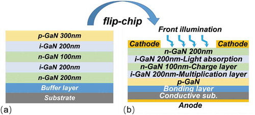
The proposed p-i-n-i-n GaN avalanche photodiode structure could be originally grown on a foreign substrate, such as silicon substrate, sapphire, or SiC. In this study, the initial epitaxial structure includes a 200 nm n-GaN layer (n = 2 × 1019 cm−3) for GaN APD, 200 nm i-GaN layer (n = 1 × 1016 cm−3), 100 nm n-GaN layer (n = 2 × 1018 cm−3), 200 nm i-GaN layer (n = 2 × 1016 cm−3) and 300 nm Mg-doped p-GaN layer (p = 2 × 1018 cm−3). Using a flip-chip and substrate removal process (Zou et al., Citation2016), a fully-vertical structure GaN APD can be achieved with the n-GaN layer as the top layer as shown in Figure ).
Figure 1. (a) Starting epitaxial structure; (b) Proposed device structure using a flip-chip and substrate removal technology.
2.1. Device simulation set up
To ensure the feasibility of simulation parameters, a simple GaN PiN diode (Zhang et al., Citation2017) was fabricated and simulated using the parameters in Table . The GaN PiN diode (with a diameter of 200 μm) consists of 2.1 μm i-layer (n = 1 × 1016 cm−3), 500 nm p-GaN (p = 1 × 1017 cm−3), and 500 nm n-GaN layer (n = 1 × 1019 cm−3). As shown in Figure , the simulated leakage current of the PiN diode matched well with the experimental results, indicating a good mapping of model parameters with the physical device parameters.
Figure 2. Comparison between experimentally measured leakage current and simulated leakage current of PiN diodes.
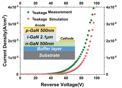
Table 1. Keys parameters used in this study
The carrier generation-recombination process mainly consists of Shockley-Read-Hall (SRH) and optical generation-recombination terms.
where and
are electron and hole lifetimes;
is the optical recombination coefficient. RSRH and ROPT are two major recombination rates of the device.
The impact ionization model (Cao et al., Citation2018) of GaN is incorporated into current continuity equations:
where ,
denotes electron and hole impact ionization coefficient, respectively;
,
,
,
are impact ionization parameters which are associated with materials and electrical field, for electrons and holes, respectively.
In this simulation work, the mobility of holes remains constant as 8 cm2/V-s, and the mobility of GaN electrons was evaluated using “high field mobility model” as follows:
where ,
were set as 400 cm2/Vs and 1.91 × 107 cm/s, respectively.
,
were set as 220 V/cm and 7, which are associated with GaN materials. The keys parameters used in this simulation are listed in the Table .
2.2. Device characteristics
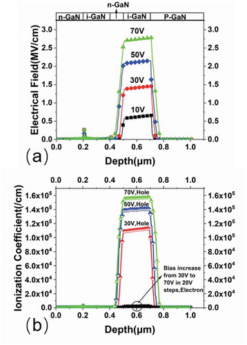
Figure displays the electrical field distribution for the flip-chip GaN p-i-n-i-n APD from reverse 10 V to reverse 70 V. When reverse biased, the electrical field is dominantly supported by the 200 nm i-GaN multiplication layer. At −70 V, the electrical filed almost reached 3 MV/cm, which is quite close to the theoretical breakdown electrical field of GaN.
According to the classical Chynoweth model, both electron and hole ionization coefficient increased exponentially as the electrical field. Figure (b) shows the calculated ionization coefficient for electrons and holes from reverse 30 V to reverse 70 V according to EquationEquations (3)(3)
(3) and (Equation4
(4)
(4) ). When a reverse voltage of 70 V or above was applied, the peak impact ionization coefficient of holes is around 1.6 × 10⁵/cm, almost two orders higher than that of electronics (2.0 × 10³/cm). Thus, multiplication process was initiated and dominated by the holes in the i-GaN multiplication layer of the flip-chip p-i-n-i-n APD.
Figure 3. (a) Electrical field distribution inside GaN APD at various reverse bias; (b) Ionization factors obtained for electrons and holes from reverse 30 V to reverse 70 V. The ionization factor of the hole is nearly two orders higher than that of electrons for the interested bias levels.
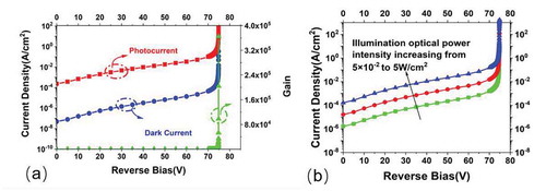
The current–voltage characteristics of GaN APDs were simulated under dark conditions and front UV illumination (λ = 340 nm), as shown in Figure (a). For reverse bias of 60 V or below, the photocurrent was gradually increased with an increasing reverse bias for GaN APD under an optical power density of 5 W/cm2. While as the reverse bias was over 75 V, currents in the flip-chip p-i-n-i-n diode started to increase rapidly, as a result of avalanche multiplication process and the breakdown voltage of 75 V was comparable with the breakdown voltage in the existing literature (Cai et al., Citation2017; Ji et al., Citation2018). The avalanche gain was calculated by the difference of the photocurrent and dark current in the breakdown region divided by the difference of average photocurrent and dark current in the non-breakdown region. The calculated avalanche gain could reach 105 for flip-chip GaN p-i-n-i-n APD. Quantum efficiency is also one of the most important parameters for avalanche photodiode. It is an important parameter to describe the photoelectric conversion capability of optoelectronic devices. It is defined that the ratio of the average number of photoelectrons produced per unit time at a particular wavelength to the number of incident photons and it was calculated as 21%. Figure (b) shows that the GaN APD showed similar responsivity and breakdown voltage for a range of illumination power density from 5 × 10⁻² W/cm2 to 5 W/cm2. The current density increase within the increasing optical power intensity in the non-breakdown region. The reason for this phenomenon is more electron-hole pairs were generated because of energy provided by high illumination power intensity.
Figure 4. (a) Reverse bias I–V characteristics illuminated by a ~ 340 nm source (optical power intensity 5 W/cm2). The photocurrent, dark current and optical gain are plotted versus reverse bias. The avalanche breakdown occurred at around 75 V; (b) Reverse bias I–V characteristics of the GaN APD. The device showed similar responsivity and breakdown voltage for various illumination power density from 5 × 10⁻² W/cm2 to 5 W/cm2.
2.3. Geiger-mode simulation
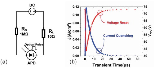
Two quenching circuits have been set-up to evaluate the capability of proposed APD working in its geiger-mode, which is useful in imaging and sensing (Deng et al., Citation2016; Ng et al., Citation2007). Figure shows the schematic of a passive quenching circuit, which is formed by series-connecting APD with two resistors, and one DC source. As the quenching resistor RQ was set to be as large as 1Mohm, the current in the circuit loop was quite small. When a short pulse of light (duration = 400 ns) was shed onto the APD, the number of carriers was increased rapidly due to multiplication and the current was increased sharply. Thus, the voltage across the resistors was increased sharply and the voltage across the APD was decreased dramatically and the avalanche process was ceased as a result of the reduced electrical field inside the device (Jackson et al., Citation2003). As the current was quenched to a certain level, the voltage across the APD was reset to a relatively high level and get ready for the next photon detection process, as shown in Figure (b). The simulation shows the current queching and voltage reset process using a purely resistive elements could be a relatively slow process, which took around 30 µs to finish.
Figure 5. (a) Passive quenching circuit scheme used for Geiger-mode APD; (b) Current quenching and voltage reset process as a function of time.
To reduce the dead-time of APD in a passive quenching circuit, an simple active quenching circuit has been used to accelerate the current quenching process in one avalanche event (Ameri et al., Citation2013; Enne et al., Citation2018; Fenker et al., Citation1992; Kim & Kim, Citation2008; Yu et al., Citation2018; Zappa et al., Citation2009). Figure (a) shows the schematic of the active quenching circuit, which adds a N-MOSFET (Vth = 0.7 V), serving as a switch and an extra current path. In addtion, the active quenching circuit uses two 1 k ohm resistors as RQ and RL, while gets rid of the extremely large resistor in the passive circuit. Figure (b) shows the current quenching process when a short pulse of light (duration = 0.4 ns) was shed onto the APD. Due to multiplication process, the current through the two resistors was increased rapidly, as a result, the voltage at Point A was increased as well to turn on N-MOSFET. Thus, the current could be drained through the N-MOSFET and speed up the quenching process. Figure (b) shows that using the active circuit, the duration to sink the current was reduced to around 15 ns, compared to 30 µs using resistive elements only. And the results suggested that the active quenching circuit had the capability of sensing very short UV light. A benchmarking table summarizing APD device performance in the existing literature and this work is shown in Table . It could be found that the breakdown voltage was comparable with those using similar voltage sustaining thickness and the circuit simulation results indicated the device in this study could offer fast response for practical UV detections.
Figure 6. (a) Active quenching circuit scheme used for Geiger-mode APD; (b) Current quenching and voltage reset process as a function of time.
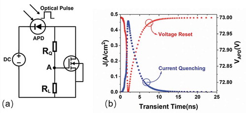
Table 2. Benchmark of GaN APD device performance
3. Conclusions
A novel GaN flip-chip p-i-n-i-n APD that integrates the merits of prevailing APDs—hole-initiated multiplication process and front-illumination is proposed and studied via TCAD-based simulation. With a 200-nm-thick multiplication layer, the calculated breakdown voltage was around 75 V (corresponding quantum efficiency of 21%) for GaN APD whose optical gain could reach 105. The capability of proposed APDs working in Geiger-mode were studied using two quenching circuits. Compared with 30 μs dead time in the purely passive quenching scheme, the active quenching scheme could markedly reduce the dead time to dozens of nanoseconds and showed the capability of sensing very short light pulse.
Correction Statement
This article has been republished with minor changes. These changes do not impact the academic content of the article.
Additional information
Funding
Notes on contributors
Xinbo Zou
Xinbo Zou received the B.E. degree from Beijing University of Posts and Telecommunications (BUPT) and Ph. D. degree from the Hong Kong University of Science and Technology (HKUST). He is currently an Assistant Professor with the School of Information Science and Technology (SIST), ShanghaiTech University. His research interest includes growth, fabrication, and characterization of GaN-based devices and nanostructures.
References
- Ameri, M., Kamrani, E., Hashemi, S., & Sawan, M. (2013, May 4–5). A fast quench-reset integrated circuit for high-speed single photon detection. 2013 IEEE international symposium on Medical Measurements and Applications (MeMeA).
- Bulmer, J., Suvarna, P., Leathersich, J., Marini, J., Mahaboob, I., Newman, N., & Shahedipour-Sandvik, F. S. (2016). Visible-blind APD heterostructure design with superior field confinement and low operating voltage. IEEE Photonics Technology Letters, 28(1), 39–9. https://doi.org/10.1109/LPT.2015.2479115
- Cai, Q., Ge, M., Xue, J., Hu, L., Chen, D., Lu, H., Zhang, R., & Zheng, Y. (2017). An improved design for solar-blind AlGaN avalanche photodiodes. IEEE Photonics Journal, 9(4), 1–7. https://doi.org/10.1109/JPHOT.2017.2725305
- Cao, L., Wang, J., Harden, G., Ye, H., Stillwell, R., Hoffman, A. J., & Fay, P. (2018). Experimental characterization of impact ionization coefficients for electrons and holes in GaN grown on bulk GaN substrates. Applied Physics Letters, 112(26), 262103. https://doi.org/10.1063/1.5031785
- Deng, S., Gordon, D., & Morrison, A. P. (2016). A Geiger-mode APD photon counting system with adjustable dead-time and interchangeable detector. IEEE Photonics Technology Letters, 28(1), 99–102. https://doi.org/10.1109/LPT.2015.2487342
- Enne, R., Steindl, B., Hofbauer, M., & Zimmermann, H. (2018). Fast cascaded quenching circuit for decreasing afterpulsing effects in 0.35-μm CMOS. IEEE Solid-State Circuits Letters, 1(3), 62–65. https://doi.org/10.1109/LSSC.2018.2827881
- Fenker, H., Oliver, J., Regan, T., & Thomas, J. (1992, October 25–31). A method to quench and recharge avalanche photodiodes for use in high rate situations. IEEE conference on nuclear science symposium and medical imaging.
- Hu, C., Zheng, X., Campbell, J. C., Onat, B. M., Jiang, X., & Itzler, M. A. (2011). Characterization of an InGaAs/InP-based single-photon avalanche diode with gated-passive quenching with active reset circuit. Journal of Modern Optics, 58(3–4), 201–209. https://doi.org/10.1080/09500340.2010.515749
- Itzler, M. A., Jiang, X., Ben-Michael, R., Nyman, B., & Slomkowski, K. (2008, February 24–28). Geiger-mode APD single photon detectors. OFC/NFOEC 2008–2008 Conference on optical fiber communication/National fiber optic engineers conference.
- Jackson, J. C., Healy, G., Kelleher, A., Alderman, J., Donnelly, J., Hurley, P. K., Morrison, A. P., & Mathewson, A. (2003, March 30–4 April). Defect passivation and dark count in Geiger-mode avalanche photodiodes. 2003 IEEE international reliability physics symposium proceedings, 2003. 41st annual.
- Ji, M., Kim, J., Detchprohm, T., Zhu, Y., Shen, S., & Dupuis, R. D. (2018). p-i-p-i-n separate absorption and multiplication ultraviolet avalanche photodiodes. IEEE Photonics Technology Letters, 30(2), 181–184. https://doi.org/10.1109/LPT.2017.2779798
- JiYuan, Z., Lai, W., Biao, H. Z., & Yi, L. (2014, August 16–23). A method to realize hole-initiated multiplication in front-illuminated GaN avalanche photodiodes. 2014 XXXIth URSI general assembly and scientific symposium (URSI GASS).
- Jones, B. K., & Kozlowski, D. A. (1993). Low frequency noise and reliability analysis of avalanche photodiodes. Quality and Reliability Engineering International, 9(4), 359–362. https://doi.org/10.1002/qre.4680090421
- Kim, K. H., & Kim, Y. S. (2008). Design and analysis of CMOS single photon counting avalanche photodiodes integrated with active quenching circuits. Journal of Nuclear Science and Technology, 45(sup5), 511–514. https://doi.org/10.1080/00223131.2008.10875903
- Liu, M., Bai, X., Hu, C., Guo, X., Campbell, J. C., Pan, Z., & Tashima, M. M. (2007). Low dark count rate and high single-photon detection efficiency avalanche photodiode in Geiger-mode operation. IEEE Photonics Technology Letters, 19(6), 378–380. https://doi.org/10.1109/LPT.2007.891939
- McClintock, R., Pau, J. L., Minder, K., Bayram, C., Kung, P., & Razeghi, M. (2007). Hole-initiated multiplication in back-illuminated GaN avalanche photodiodes. Applied Physics Letters, 90(14), 141112. https://doi.org/10.1063/1.2720712
- Ng, J. S., Tan, C. H., Rees, G. J., & David, J. P. R. (2007). Effects of dead space on breakdown probability in Geiger mode avalanche photodiode. Journal of Modern Optics, 54(2–3), 353–360. https://doi.org/10.1080/09500340600753814
- Osinsky, A., Shur, M. S., Gaska, R., & Chen, Q. (1998). Avalanche breakdown and breakdown luminescence in p-/spl pi/-n GaN diodes. Electronics Letters, 34(7), 691–692. https://doi.org/10.1049/el:19980535
- Pau, J. L., Bayram, C., McClintock, R., Razeghi, M., & Silversmith, D. (2008). Back-illuminated separate absorption and multiplication GaN avalanche photodiodes. Applied Physics Letters, 92(10), 101120. https://doi.org/10.1063/1.2897039
- Qiu, X., Song, Z., Sun, L., Zhang, Z., Lv, Z., Wen, Q., & Jiang, H. (2019). High-gain AlGaN/GaN visible-blind avalanche heterojunction phototransistors. Journal of Materials Science: Materials in Electronics, 31(1), 652–657.
- Verghese, S., McIntosh, K. A., Molnar, R. J., Chen, C., Molvar, K. M., Melngailis, I., & Aggarwal, R. L. (1998, June 22–24). GaN-based avalanche photodiodes. 56th annual device research conference digest (Cat. No.98TH8373).
- Verghese, S., McIntosh, K. A., Molnar, R. J., Mahoney, L. J., Aggarwal, R. L., Geis, M. W., Molvar, K. M., Duerr, E. K., & Melngailis, I. (2001). GaN avalanche photodiodes operating in linear-gain mode and Geiger mode. IEEE Transactions on Electron Devices, 48(3), 502–511. https://doi.org/10.1109/16.906443
- Wanyan, J., Sun, Z., Shi, S., Wu, M., He, G., & Li, G. (2013, August 19–22). Dependence of electrical field and photoresponse on multiplication region thickness for GaN APDs. 2013 13th international conference on Numerical Simulation of Optoelectronic Devices (NUSOD).
- Yu, Y., Wang, C., Shi, H., Yang, B., & Liu, X. (2018, August 5–8). A review of quenching circuit design based on Geiger-mode APD. 2018 IEEE International Conference on Mechatronics and Automation (ICMA).
- Yuan, Z., Lai, W., Hao, B., & Yi, L. (2014). A method to realize hole-initiated multiplication in front-illuminated GaN avalanche photodiodes. URSI General Assembly and Scientific Symposium (URSI GASS).
- Zappa, F., Tosi, A., Mora, A. D., & Tisa, S. (2009). SPICE modeling of single photon avalanche diodes. Sensors and Actuators. A, Physical, 153(2), 197–204. https://doi.org/10.1016/j.sna.2009.05.007
- Zhang, X., Zou, X., Lu, X., Tang, C. W., & Lau, K. M. (2017). Fully- and Quasi-vertical GaN-on-Si p-i-n diodes: High performance and comprehensive comparison. IEEE Transactions on Electron Devices, 64(3), 809–815. https://doi.org/10.1109/ted.2017.2647990
- Zou, X., Zhang, X., Lu, X., Tang, C. W., & Lau, K. M. (2016). Fully vertical GaN p-i-n diodes using GaN-on-Si epilayers. IEEE Electron Device Letters, 37(5), 636–639. https://doi.org/10.1109/led.2016.2548488