
 ?Mathematical formulae have been encoded as MathML and are displayed in this HTML version using MathJax in order to improve their display. Uncheck the box to turn MathJax off. This feature requires Javascript. Click on a formula to zoom.
Abstract
Effect of LaCl3 concentration on the electrical conduction mechanism of LaF3/porous silicon (PS) structure has been investigated in this work. LaF3 layers have been deposited by a novel chemical bath deposition (CBD) technique. With this simple technique, LaF3 produced as LaCl3 are made to react with hydrofluoric (HF) acid on the porous silicon substrate. This enables direct deposition of LaF3 on the pore walls of the porous silicon leading to a successful passivation of PS. The compositions of the deposited LaF3 were confirmed by Energy Dispersive of X-ray (EDX) analysis. The electrical conduction study has been done by impedance analyzer (HP4294A). From this study it can be concluded that the conductance increases with LaCl3 concentration but decreases for higher concentration.
Public Interest Statement
Recently, there has been increasing interest in semiconductor materials, which find applications in optoelectronic, photovoltaic industries, and photoelectrochemical solar cell devices. Among these materials, LaF3 thin films appear to be promising candidates for many technological applications.
Over the years, many passivation methods have been attempted to improve the stability, as well as efficiency, of PS. However, these passivation methods always carry the danger of a total oxidation of the PS layer and of transforming it into SiO2. The chemical bath deposition method (in our work) is simple and removes all mentioned disadvantages.
On the other hand, the passivating layer of LaF3 on PS can be optimized according to conductance by LaCl3 concentration because the concentration of LaCl3 dominates the LaF3 layer and hence conduction mechanism. This LaF3/PS structure with optimum LaF3 thickness could provide enhancement and stabilization of conduction, which is very important for PS to be a potential material in the fabrication of electronic and optoelectronic devices.
1. Introduction
Recently, there has been increasing interest in semiconductor materials, which find applications in optoelectronic, photovoltaic industries, and photo-electrochemical solar cell devices. Among these materials, LaF3 thin films appear to be promising candidates for many technological applications due to their stability, band gap energy (about 10.3 eV) (Pilvi, Puukilainen, Arstila, Leskelä, & Ritala, Citation2008), transparency, and photoconductor behavior. A disadvantage of this material is the aging, that is, the slow spontaneous oxidation of porous silicon (PS) (Boukherroub, Morin, Wayner, & Lockwood, Citation2000). Porous silicon, PS can be considered as a silicon (Si) crystal having a network of voids in it (Pap, Citation2005). This chemical conversation is slow and basically similar to the aging of Si wafer, i.e. a native oxide layer forms on the surface of the pores and the thickness of this oxide layer grows with time. Due to the aging effect, the structural, compositional, electrical, and optical properties of PS show continuous change with storage time (Boukherroub et al., Citation2000). That is many of its properties, such as photoluminescence, are age dependent and unstable. Tischier et al. observed that the exposure of PS in different ambient results in a rather rapid decrement of photoluminescence (PL) intensity (Fan, Citationn.d.). One possible way to reduce the aging effect could be “passivation” of PS by an active material surface to reduce the chemical reactivity of the surface and protect it against contamination and increase its stability by isolating the surface from chemical and electrical conditions in the environment. Over the years, many passivation methods, such as anodic oxidation and rapid thermal oxidation, have been attempted to improve the stability, as well as efficiency, of PS. However, these passivation methods always carry the danger of a total oxidation of the PS layer and of transforming it into SiO2. Because of various advantages of LaF3 like good moisture resistance (Hopkins, Hoffman, & Kramer, Citation1975), large bad (Pilvi et al., Citation2008), passivation of porous silicon has been investigated for the first time in our previous articles (Al Mortuza, Rahman, Mou, Nain, & Ismail, Citation2012). By reacting LaCl3 with hydrofluoric acid (HF), LaF3 has been tried to deposit in to the pores of porous silicon (PS) surface with a goal of not to allow the PS sample to be oxidized during transportation and drying for passivation like other deposition techniques (Al Mortuza et al., Citation2012). Electrical conduction of LaF3 passivated porous silicon structure changes with LaCl3 concentration. It is because the structure has capacitive properties which depend upon dielectric material as well as frequency. The capacitance changes with LaCl3 concentration (Rahman, Mou, & Ismail, Citation2011). As a result, the thickness of dielectric material changes and the conductivity will also change. The conductance will increase if the frequency increases. This article investigates the influence of LaCl3 concentration on the variation of conductance (G) of chemical-bath-deposited LaF3/PS structure.
2. Experimental
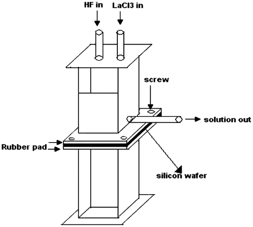
The porous silicon has been prepared in the homemade double-tank cell by anodic etching of silicon wafer (Halimaoui, Citation1997) as shown in Figure . The anodic etching of Si was done in a 1:1 (as the Si substrate was n-type) solution of 48% HF in absolute ethanol. The LaF3 films with different LaCl3 concentration were prepared. The same double-tank chamber in the upright position is used for LaF3 deposition (Figure ).
Figure 1. Schematic drawing of a double-tank chamber for PS fabrication.
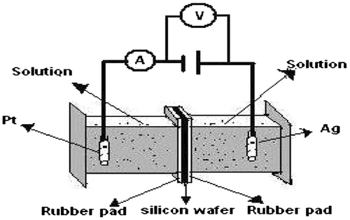
Figure 2. Double-tank chamber in upright position for chemical-bath deposition of LaF3.
Just after the anodic etching, the etching solution was drained out and the fresh HF was introduced in the chamber to wash out any remaining etching solution on the chamber. After draining out the washing HF, solution of LaCl3 and 48% HF were introduced simultaneously into the etching chamber to initiate the chemical reaction and produces LaF3 that deposits on the just prepared PS sample. Thus, the PS is never exposed to the environment before passivation and this CBD method of LaF3 deposition should prevent the PS to be oxidized. The Conductance–Voltage (G-V) characteristics of LaF3-deposited PS samples were determined for different samples. The chemical composition of the samples was determined by the Energy Dispersive of X-ray (EDX) analysis using S-3400 N SEM.
Anodic etching was carried out using an electrolyte of HF (48%) and ethanol (98%) in 1:1 proportion under a constant current density of 15 mA/cm2 for 30 min at room temperature. The electrochemical anodization of Si wafer was done using a double-tank cell setup (Al Mortuza et al., Citation2012). The wafer was cut into pieces and these pieces of Si wafer were cleaned by successively immersing in acetone, ethanol, and deionized water. The electrolyte consisted of HF:C2H5OH in the ratio of 1:1 by volume. After 30 min-anodization, the etching solution and back contact solution were drained out, keeping the samples in the etching chamber (Halimaoui, Citation1997). Fresh HF was then introduced into the chamber to wash out any remaining etching solution on the chamber. After draining out the HF that used for washing, 0.2, 0.4, and 0.6 solution of LaCl3 and 48% HF were introduced simultaneously into the etching chamber through the “HF in” and “LaCl3 in” channels to do the chemical reaction. The chemical reaction that produces LaF3 is pretty simple, at room temperature, the addition of hydrofluoric acid to an aqueous solution of lanthanum chloride precipitates out lanthanum fluoride, LaF3 (Patnaik, Citation2002, p. 448). The formation of white precipitate (LaF3) confirmed the mechanism of film formation. The basic reaction during LaF3 deposition is given below:
The solution inside the etching chamber was stirred for 10 s and resulting LaF3 crystals were allowed to passivate the PS layer for 4 min. After each cycle of reaction, the solution was drained out through the “Solution out” channel and a new solution was introduced into the chamber for the next deposition cycle. In this case, the deposition results from a chemical reaction in solution, which may involve the surface silicon atoms, and in this case, we will speak of chemical grafting of the surface, and the reaction is limited to the formation of monolayer (Hérino, Citation2000). The whole process was repeated to obtain the various thickness of LaF3 on to PS. After completing the required cycle, the wafer was removed from the chamber, rinsed with de-ionized water, and dried in air at room temperature. The prepared samples were annealed at 600°C temperature. For Conductance-Voltage (G-V) characterization of the lanthanum fluoride-deposited PS sample, silver (Ag) film was evaporated onto the front and backside of the sample in a small area using Edwards E-306A vacuum coating unit. Then, the Conductance-Voltage (G-V) study was done by an impedance analyzer (HP 4294A) in room temperature and in a dark chamber.
3. Results and discussion
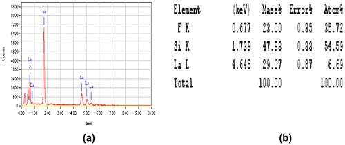
The chemical-bath-deposited LaF3 on porous silicon produces a heterostructure system (LaF3/PS/Si). The SEM images before and after deposition of LaF3 are shown in Figure to see the surface structure of PS. The compositions of the deposited LaF3 were confirmed by Energy Dispersive of X-ray (EDX) analysis. The EDX spectra and the elemental concentrations of 0.4 M LaCl3 sample with 600°C annealing temperatures are shown in Figure (a) and (b), respectively.
Figure 3. SEM image of a macro-porous Si sample (a) before (Ossicini, Pavesi, & Priolo, Citation2003) and (b) after deposition of LaF3.
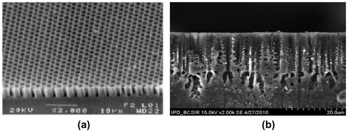
Figure 4. (a) EDX spectra and (b) elemental concentration of 0.4 M LaCl3 samples with 600°C annealing temperature.
The G-V characteristics of LaF3 passivated PS samples with different LaCl3 concentrations are illustrated in Figure .
Figure 5. G-V variation of LaF3 passivated 600°C annealed PS samples with (a) 0.2, (b) 0.4 and (c) 0.6 M LaCl3 concentration for different frequencies.
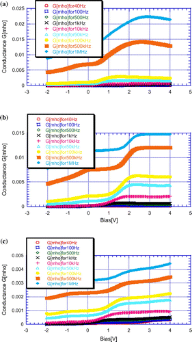
From Figure , it is clear that conductance of LaF3 passivated porous silicon sample varies with LaCl3 concentrations as well as frequencies. The variations of conductance with LaCl3 concentrations as well as with frequencies are shown in Figures and , respectively.
Figure 6. Variation of conductance of 600°C annealed LaF3 passivated PS sample with different LaCl3 concentrations at the frequency of 1 kHz.
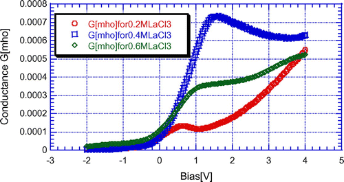
Figure 7. Variation of conductance with frequencies for LaF3 passivated PS samples with 0.2 and 0.4 M LaCl3 at 600°C annealing temperature.
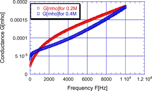
From Figure , it is clear that the peak value of conductance increases with LaCl3 concentration but decreases for higher concentration. It may due to be the increment and decrement of LaF3 layer thickness. From Figure , it is clear that the conductance value of any sample increases with frequencies because the capacitive reactance decreases with frequency.
In this report, LaF3 was deposited on PS by CBD technique with a homemade double-tank cell setup. From the EDX data, it was confirmed that the LaF3 was deposited on PS in the in situ technique. Later the influence of LaCl3 concentration on the conduction mechanism of LaF3/PS structure has been investigated. The peak value of conductance increases with LaCl3 concentration but decreases for higher concentration.
4. Conclusions
In this paper, we attempted to evaluate the conductance of chemical-bath-deposited porous silicon structure. This investigation allowed us to determine the conductance through heterojunction interface. The aim of this work was to investigate the influence of LaCl3 concentration on the conduction mechanism of chemical-bath-deposited LaF3/porous-silicon structure. The EDX confirmed the deposition of LaF3 on PS. Hence, from this research, it can be concluded that LaF3 can be efficiently deposited on PS by the CBD technique.
From these experimental results, it can also be concluded that the passivating layer of LaF3 on PS can be optimized according to conductance by LaCl3 concentration because the concentration of LaCl3 dominates the LaF3 layer and hence conduction mechanism. This LaF3/PS structure with optimum LaF3 thickness (which depends on LaCl3 concentration) could provide enhancement and stabilization of conduction which is very important for PS to be a potential material in the fabrication of electronic and optoelectronic devices.
Funding
This work has been partially supported by the COMSTEC research grant, Rajshahi University and University Grants Commission (UGC), Dhaka, Bangladesh.
References
- Al Mortuza, A., Rahman, M. H., Mou, S. S., Nain, M. J., & Ismail, A. B. M. (2012, August). Passivation of porous silicon by LaF3 using a simple single-source chemical bath technique. International Journal of Materials and Chemistry, 2, 111–115.10.5923/j.ijmc.20120203.05
- Boukherroub, R., Morin, S., Wayner, D. D. M., & Lockwood, D. J. (2000). Thermal route for chemical modification and photoluminescence stabilization of porous silicon. Physica Status Solidi (A), 182, 117–121.10.1002/(ISSN)1521-396X
- Fan, Y. (n.d.). Shanghai: School of Materials Science and Engineering, Shanghai University.
- Halimaoui, A. (1997). Porous silicon formation by anodisation. In L. T. Chanham (Ed.), Properties of porous silicon (pp. 12–13). London: IEE INSPEC, The Institution of Electrical Engineers.
- Hérino, R. (2000). Nanocomposite materials from porous silicon. Materials Science and Engineering: B, 69–70, 70–76.10.1016/S0921-5107(99)00269-X
- Hopkins, R. H., Hoffman, R. A., & Kramer, W. E. (1975). Moisture resistant optical films: Their production and characterization. Applied Optics, 14, 2631.10.1364/AO.14.002631
- Ossicini, S., Pavesi, L., & Priolo, F. (2003). Porous silicon (Vol. 194, pp. 75–122). Springer-Verlag Berlin Heidelberg.
- Pap, A. E. (2005). Investigation of pristine and oxidized porous silicon (Doctoral Dissertation). Oulu: Faculty of Technology, University of Oulu. Retrieved from http://herkules.oulu.fi/isbn9514277759/
- Patnaik, P. (2002). Handbook of inorganic chemicals. New York, NY: McGraw-Hill Professional.
- Pilvi, T., Puukilainen, E., Arstila, K., Leskelä, M., & Ritala, M. (2008). Atomic layer deposition of LaF3 thin films using La(thd)3 and TiF4 as precursors. Chemical Vapor Deposition, 14, 85–91.10.1002/(ISSN)1521-3862
- Rahman, M. H., Mou, S. S., & Ismail, A. B. M. (2011, December ). Fabrication and characterization of lanthanum fluoride (LaF3)-passivated porous silicon (PS) structure prepared by chemical bath deposition technique. Journal of Scientific & Technical Research, 1, 97–101.