
 ?Mathematical formulae have been encoded as MathML and are displayed in this HTML version using MathJax in order to improve their display. Uncheck the box to turn MathJax off. This feature requires Javascript. Click on a formula to zoom.
Abstract
The scheme to realize high-speed (~250 Gb/s) all-optical Boolean logic gates using semiconductor optical amplifiers with quantum-dot (QD-SOA) is introduced and analyzed in this review. Numerical simulation method was presented by solving the rate equation and taking into account nonlinear dynamics including carrier heating and spectral hole-burning. Binary phase shift keyed signal and on–off keyed signal are used to generate high-speed all-optical logic gates. The applications based on all-optical logic gates such as, all-optical latches, pseudo random bit sequence generation, and all-optical encryption, are also discussed in this review. Results show that the scheme based on QD-SOA is a promising method for the realization of high-speed all-optical communication system in the future.
Public Interest Statement
The current optical communication system does not work entirely in optical domain. A larger amount of the switches and data processors are made of electrical circuits which limits the ultimate speed of the existing optical transmission system. One promising solution is all-optical packet switching networks in which the header recognizing, payload processing, buffering, and forwarding of optical packets are all carried out in the optical domain, bringing together the wide fiber bandwidth and high routers forwarding capacity. The key building blocks of all-optical switching network are the all-optical circuits.
These proposed and studied all-optical circuits based on next generation quantum dot devices are the building blocks of the future all-optical network. These all-optical circuits design and simulation are of fundamental importance to the future generation of optical communication systems. These designed all-optical circuits are promising candidates to replace the discrete electrical counterparts currently used in communication systems.
1. Introduction
In future high-speed optical communication systems, logic gates will play important roles, such as signal regeneration, addressing, header recognition, data encoding, and encryption (Li, Citation2015). In recent years, people have demonstrated optical logic using different schemes, including using dual semiconductor optical amplifier (SOA) Mach–Zehnder interferometer(MZI) (Kim et al., Citation2002; Wang et al., Citation2004), semiconductor laser amplifier (SLA) loop mirror (Houbavlis et al., Citation1999), ultrafast nonlinear interferometer (UNI) (Bintjas et al., Citation2000), four-wave mixing (FWM) in SOA (Chan, Chan, Chen, & Tong, Citation2004), and cross gain (XPM)/cross phase (XPM) modulation in nonlinear devices (Li et al., Citation2005). Among above schemes, the SOA-based MZI has the advantage of being relatively stable, simple, and compact. However, optical logic gates have been demonstrated at 40 Gb/s (Webb, Manning, Maxwell, & Poustie, Citation2003) and demultiplexing at 160 Gb/s (Diez, Schubert, Ludwig, & Ehrke, Citation2000) using regular SOA-based Mach–Zhender interferometer. In order to realize higher speed data processing, faster device and schemes are needed. The emergence of semiconductor optical amplifiers with quantum dot active region, i.e. optical amplifiers with quantum-dot (QD-SOA), in recent years, provides a faster device for signal processing. QD-SOAs have high saturated output power, low noise figure (Li, Ma, Hu, & Dutta, Citation2012a), fast carrier relaxation rate between QD energy states (Berg & Mork, Citation2004; Li, Hu, & Dutta, Citation2013a) and a much smaller carrier heating impact on gain and phase recovery times (Reithmaier & Eisenstein, Citation2008) which makes them suitable for high-speed Boolean logic operations.
The current optical communication system does not work entirely in optical domain. A larger amount of the switches and data processors are made of electrical circuits which limits the ultimate speed of the existing lightwave transmission system. One promising solution is all-optical packet switching networks in which the header recognizing, payload processing, buffering, and forwarding of optical packets are all carried out in the optical domain, bringing together the wide fiber bandwidth and high routers forwarding capacity (Dorren et al., Citation2003). In addition, the security of information is very important and all-optical encryption and decryption can be used to protect the information for future all-optical communication system. The key building blocks of optical switching and encryption are the all-optical Boolean logic gates, include XOR, AND, OR, NAND, NOT, and functional circuits built using these gates such as optical latches. Thus, it is very important to build all-optical logic gates capable for high speed and high output quality.
In order to further enhance operation speed of all-optical logic gates, besides using QD-SOA, the other method involves in the use of two-photon absorption (TPA) effect which is an ultrafast nonlinear process of SOA. With a high-intensity pump light injected into SOA, a fast changing TPA-induced phase shift becomes dominant in the total phase change experienced by a weak probe signal. As a result, the SOA will quickly respond to the injected short pulse in the active region which makes it suitable for high-speed operation. Several researches have demonstrated that all-optical logic gates based on TPA effect in common bulk SOA are capable of handling data at speed up to 250 Gb/s (Li, Ma, Hu, & Dutta, Citation2012b; Zhang, Li, Hu, & Dutta, Citation2015a, Citation2015b). However, the method using TPA effect needs a very high-intensity pump light usually with ultrashort pulse width (Hu, Zhang, Li, & Dutta, Citation2016; Li et al., Citation2016; Zhang, Hu, Li, & Dutta, Citation2016) which increases the expense and complexity of practical all-optical system. In order to obtain better output quality of all-optical logic gates, binary phase shift keyed (BPSK) signal instead of on–off keyed (OOK) signal can be used to realize all-optical logic gates. Because BPSK signals carry information on the phase part while keeping the amplitude as a constant, the impairments from optical nonlinear effects and amplified spontaneous emission are greatly reduced.
2. All-optical logic gates based on QD-SOA
In this part, a model which simulates two QD energy level carrier dynamics and nonlinear effects affecting the gain spectrum of the device is presented. Using this model, a more accurate simulation of fast all-optical logic gates including AND, XOR, and NOT is provided. The effect of device induced ASE noise is also discussed.
2.1. QD-SOA structure and rate equations
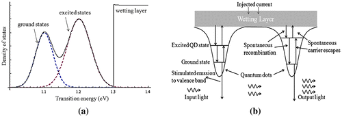
The commonly used QD-SOA is InAs/GaAs, with InAs Stranski–Krastanov (SK) quantum dots embedded in GaAs layer (Akiyama, Wada, et al., Citation2000; Mukai et al., Citation1998). This type of device can provide ~15 dB gain at wavelength 1550 nm with noise figure as low as 7 dB (Berg & Mork, Citation2004). The active layer of the device consists of alternately stacked InAs island layers and GaAs intermediate layers. This configuration can significantly increase areal dot density and the modal gain of the SOA (Li et al., Citation2016) and the gain is nearly polarization independent (Ridha, Li, Rossetti, Patriarche, & Fiore, Citation2008). The density of state of the InAs/InGaAsP/InP QD-SOA (Berg & Mørk, Citation2003) is shown in Figure (a). From the graph, we see the carriers in the QD’s are mostly populated on two groups of almost discrete energy levels (simplified here as two discrete states: QD ground state and QD excited state). The wetting layer has a continuous set of energies, supplying the two levels with carriers through interstate transitions and is able to refill itself using external electric current injection. The transition among the wetting layer, the QD excited state (ES), and the QD ground state (GS) is schematically illustrated in Figure (b). The GaAs layer is the “wetting layer” in Figure which used to feed the ground state and excited state with carriers through interstate recombination. External current is applied to the device and mostly accumulated in the wetting layer.
Figure 1. (a) The QD-SOA density of states as a function of transition energy. (b) The transition diagram of InAs/InGaAsP/InP QD-SOA.
Rate equations are used to describe gain and phase dynamics in QD device (Li, Hu, & Dutta, Citation2013b). The carrier density dynamics can be described as:(1)
(1)
(2)
(2)
(3)
(3)
where w, h, and f are the occupation probabilities of the wetting layer, the QD excited state, and ground state, respectively; Nwm, Nesm, and Ngsm are the maximum possible carrier densities of each state; Гd is the active layer confinement factor, I is the injected current, V is the effective volume of the active layer, a is differential gain, S(t) is photon density in the active region.
The gain dynamics in the QD-SOA include the contribution from the carrier density pulsation dynamics and nonlinear processes including carrier heating (CH) and spectral hole-burning (SHB) effect. Generally, the linear part of gain coefficient is based on the stimulated emission from the QD ground state to the valence band,(4)
(4)
where Nt is the transparent carrier density of the QD ground state. The suppression of the gain coefficient brought by nonlinear CH and SHB effects can be expressed as:(5)
(5)
To a first approximation, ΔgCH and ΔgSHB are proportional to instantaneous light intensity S(t).(6)
(6)
(7)
(7)
where εCH and εSHB are the gain suppression factors of carrier heating and spectral hole-burning effect, respectively. From Equations (5)–(7), we can get (Akiyama, Kuwatsuka, et al., Citation2000):(8)
(8)
The injected light and changed temperature result from carrier heating also changes the refractive index of the active region, and thus a phase change to any probe wave injected.(9)
(9)
where Gl(t) = eg(t)l is the gain factor of the device with l being the effective length of the active layer, α and αCH are the linewidth enhancement factor of the device.
2.2. Principles of QD-SOA-MZI-based all-optical logic gates
A QD-SOA-based Mach–Zehnder interferometer can be used to realize all-optical XOR, AND, NOT operations. As is shown in Figure , two identical QD-SOAs are in the two arms of the interferometer, three optical data streams carried by different wavelengths are injected into the two arms, where the control beam at λ2 is symmetrically split into two branches at port C and guided into the two arms separately. The two beams then interact with data stream A, B and will experience a modulated gain and phase via XGM and XPM processes.
Figure 2. Schematic of a QD-SOA-based Mach–Zehnder Interferometer.
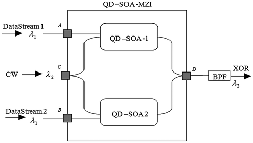
The light in two beams will combine and interfere at port D, after screening the other wavelengths using a band-pass filter (BPF), the output power at wavelength λ2 can be expressed as:(10)
(10)
where Pcb is the control beam power at port C, we can tune the initial phase difference between the two arms by (for example,) adding a tunable phase shifter in one of the arms. For our logic gates used here, we typically tune
= π so that Equation (10) becomes:
(11)
(11)
2.2.1. XOR logic gate
Set control beam as clock wave at the same repetition rate as data A and B, the QD-SOA MZI will function as a XOR logic gate. When A = B = 0 or A = B = 1, the control beams in each arm will see the same cross gain or phase modulation as they go through the QD-SOA. And the output branches of the control beam will have a destructive interference pattern at output because of the initial π phase difference, and the output will be 0 at wavelength λ2. When A and B are not the same, the branches of control beam will undergo different gain, we can have a constructive interference at output port if we can change the power of modulating data streams A and B to make = π, in this case the output will be 1 for wavelength λ2.
2.2.2. AND logic gate
In order to realize AND operation, a scheme similar to Dong, Sun, Wang, Dutta, and Jaques (Citation2006) can be used: data A and a continuous wave (CW), both at wavelength λ1, are injected into each of the two QD-SOAs. Set the power of the CW so that it is the same as the average background optical power to balance the gain and phase impact from the “0” data components, data stream C at wavelength λ2 is injected to both arms as control beam, this configuration will provide a process which gives “1” at output at λ2 only when both data A and C is “1,” functionally the same as all-optical AND gate.
2.2.3. NOT logic gate
Similar to XOR gate, if we change data stream B into a clock wave at wavelength λ1, we will have the setup of an all-optical NOT logic gate, which gives inversed value of data stream A at wavelength λ2 at the output.
2.3. The role of amplified spontaneous emission (ASE) noise
As the pulse trains go through the amplifier, spontaneous emission will be added to the initial wave pattern in the form of white noise. This noise will reduce the signal to noise ratio, the effect is quantitatively described by the noise figure of the amplifier:(12)
(12)
With SNRin and SNRout are corresponding to the signal to noise ratio at the input and output, respectively.
2.4. Simulation results and output quality study
The simulated result can be obtained by solving rate Equations (1)–(3) and setting input light beam power within non-saturated regime. Results of XOR, AND, OR logic operations are shown in Figures –, respectively (Ma, Chen, Sun, & Dutta, Citation2010), 27 − 1 pseudo random bit sequence (PRBS) data signals are used as input. The output eye diagram is also plotted as inset in each figure to show qualitatively the output quality. Quantitative quality evaluation can be done using quality factor method, as described below.
Figure 3. A side-by-side comparison of XOR result for (a) 40 Gb/s and (b) 250 Gb/s XOR operation, insets are the simulated eye diagram of the output wave.
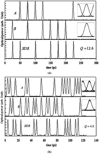
Figure 4. Simulated result for all-optical AND gate operating at 250 Gb/s.
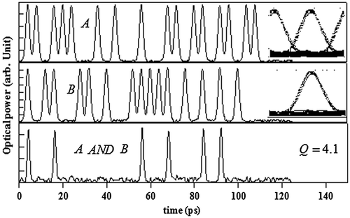
Figure 5. Simulated results for all-optical NOT gate operating at 250 Gb/s.
The quality factor for the output data waveform can be expressed as, Q = (S1 − S0)/(σ1 + σ0) where S1 and S0 are the average value for all the out coming “1” and “0” data’s peak power, respectively; σ1 and σ0 are their standard deviations. The quality factor is related to the gate’s bit-error rate (BER) in terms of .
Since the mechanism for the three different types of logic gates are basically the same, similar output quality for different gates can be obtained at a certain repetition rate. And the quality of this scheme is evaluated without relating to any specific logic operation.
The calculated quality factor shows significant dependence on injected current density, pulse width, transition lifetime from QD excited state to ground state τe−g and single pulse energy. Figure shows the contribution to output quality from injected current and pulse width, at high logic operation bit rate, input single pulse energy is set to 0.5 pJ to make sure the operation takes place in the non-saturated regime of the QD-SOA. From the results we find that at low injected current density level (J < 1.8 kA/cm2), the Q factor is lower and will increase rapidly with increased current density. This can be explained as follows: with increased current density, more carriers are injected to the wetting layer, thus each energy level in the quantum dot can recover faster to initial carrier density level after carrier depletion following optical pulse injection and amplification. This reduces the pattern effect considerably. For very high current density Q values saturate. The smaller pulse width (less energy and hence less carrier depletion) also results in better performance (higher Q value).
Figure 6. Calculated operation quality factor Q at different pulse width and injected current density, single pulse energy is set to 0.5 pJ. (a) 250 Gb/s XOR operation (b) 160 Gb/s operation.
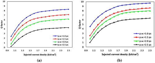
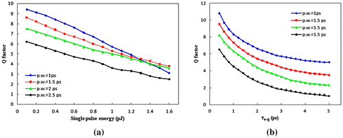
Figure shows the calculated Q factor as a function of single pulse energy and carrier transition lifetime between QD excited state and ground state. The calculation is done with an injected current density of 1.8 kA/cm2. From the results, we see a decrease in output quality (Q factor) with the increase in single pulse energy of the input data and τe−g. As single pulse energy increases, the carrier density of the active region of the device is depleted more, thus it takes longer to recover to initial level. The transition lifetime determines the speed of gain and phase recovery speed in the active region, thus Q-factor is higher for shorter transition times for high-speed operation.
Figure 7. Calculated 250 Gb/s operation quality factor Q at different single pulse energy and transition lifetime from QD excited state to ground state. Injected current density is set to 1.8 kA/cm2. (a) Q factor dependence on single pulse energy (b) Q factor dependence on ES to GS transition lifetime.
3. All-optical logic gates using BPSK signal based on QD-SOA
Although all-optical logic gates using OOK signals based on QD-SOA-MZI have been proved at data rates of ~250 Gb/s the patterning effects and amplified spontaneous emission are very strong for the schemes using OOK signal which will degrade the output quality. Thus, an alternative method of improving the output quality and achieving high-speed all-optical logic operations has been proposed (Li, Hu, & Dutta, Citation2014; Li, Hu, Zhang, & Dutta, Citation2015). This method utilizes a QD-SOA-MZI pair each differentially driven by a data input and its complement.
3.1. Operation principles of all-optical logic gates using BPSK signal
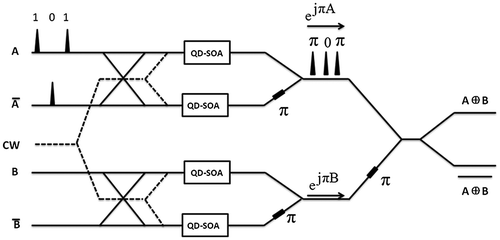
The proposed scheme accomplishing all-optical XOR operations is shown in Figure . It consists of a pair of QD-SOA-MZIs. Each QD-SOA-MZI is differentially driven by data and complement. The arrangement in Figure , in contrast to the conventional single SOA-MZI XOR setup, ensures that each QD-SOA receives a nearly constant-power stream of input pulse train. This is also illustrated in Figure using an example of an on–off keyed (OOK) signal A = [101]. Hence, the patterning effects can be mitigated that arise from the fluctuation in the signal optical powers when QD-SOAs are directly modulated by OOK signals without a differential setup. For instance, the most deleterious situation is avoided, where the QD-SOAs receive a long sequence of 1’s followed by a long sequence of 0’s, or vice versa. Furthermore, because BPSK signals carry information on the phase part while keeping the amplitude as a constant, the impairments from optical nonlinear effects and amplified spontaneous emission are greatly reduced. The working principle as follows: the top QD-SOA-MZI converts the input OOK data streams A and its complement into BPSK signal, exp(jπA). The bottom QD-SOA-MZI similarly outputs a BPSK signal exp(jπB). The conversion of OOK into BPSK was first used for all-optical wavelength conversion of DPSK signals and its process is detailed in Kang et al. (Citation2005, Citation2008). The next step in XOR operation is the linear optical interference between these two BPSK signals. The interference yields two OOK signals, one is XOR logic and the other is NXOR logic. The intensity envelops of the output signals emerging from the constructive and destructive ports of the 2x2 coupler are calculated using:(13)
(13)
(14)
(14)
Figure 8. Schematic of the all-optical XOR logic gate, CW: continuous wave.
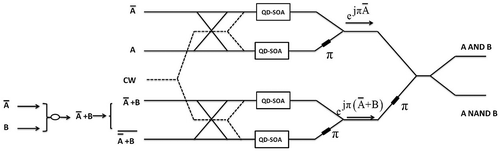
We can use a similar scheme to realize logic AND and NAND operations as shown in Figure . From Boolean algebra, we know . In this scheme, the top QD-SOA-MZI converts the input OOK data
and its complement A into BPSK signal exp(jπ
).The bottom QD-SOA-MZI similarly outputs a BPSK signal exp(jπ(
+ B)). Thus, one output after interference is
which is the same as A AND B and the other output after interference is A NAND B.
is simply realized by an optical coupler.
Figure 9. Schematic of the all-optical AND and NAND logic gates, CW: continuous wave.
3.2. Numerical simulation results
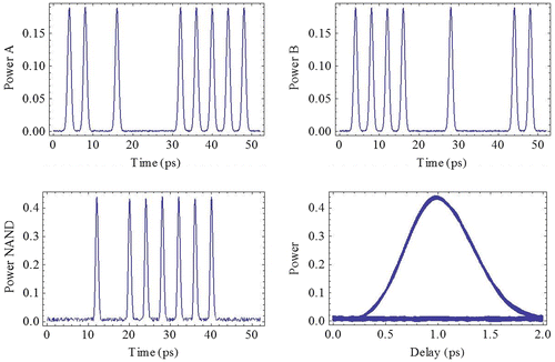
Simulated results of all-optical XOR, AND, and NAND logic gates using the schemes in Figures and are shown in Figures – (Li et al., Citation2014, 2015). The output eye diagrams are also plotted to show the output quality. From the simulated results, it is shown that all-optical XOR, AND, and NAND logic gates using BPSK signal, scheme of a pair of QD-SOA-MZIs, @ ~250 Gb/s are feasible and have improved output quality.
Figure 10. Data A and Data B are shown on the top. Simulated results of output (XOR) and eye diagram of the output are shown below.
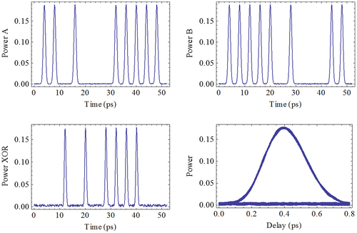
Figure 11. Data A and Data B are shown on the top. Simulated results of output (AND) and eye diagram of the output are shown below.
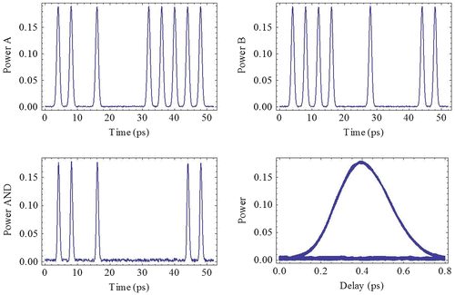
Figure 12. Data A and Data B are shown on the top. Simulated results of output (NAND) and eye diagram of the output are shown below.
4. All-optical latches using QD-SOA
All-optical latches are important for a wide range of applications including communication systems, optical random access memory (RAM), and encryption. For communication system, it can be used for SONET scrambling and descrambling. The basic optical latches are the Set-Reset latch and the D-Flip-Flop. Both of these types of devices can be built using all-optical Boolean logic operations such as NAND and NOT. These operations are also important for all-optical signal processing such as bit pattern matching, PRBS generation, and label swapping.
4.1. Schematic of all-optical latches and QD-SOA structure
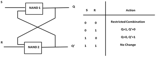
The Set-Reset Latch is considered as one of the most basic logic circuit possible. This simple latch is basically a one-bit memory bistable device that has two inputs, one of which will “SET” the device (meaning the output = “1”), and another which will “RESET” the device (meaning the output = “0”). Then the SR description stands for “Set-Reset.” The reset input resets the flip-flop back to its original state with an output Q that will be either at a logic level “1” or logic “0” depending upon this set/reset condition. The simplest way to make Set-Reset Latch is to connect together a pair of cross-coupled 2-input NAND gates. The schematic of Set-Reset Latch and the truth table for the Set-Reset function are showed in Figure .
Figure 13. The left figure is the schematic of the Set-Reset Latch. The right figure is the truth table for the Set-Reset function.
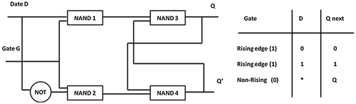
The D-Flip-Flop is also widely used as the building block of a logic circuit. It is also known as a data or delay flip-flop. The D-Flip-Flop captures the value of the D-input at a definite portion of the gate cycle (such as the rising edge of the gate pulse). That captured value becomes the Q output. At other times, the output Q does not change. The D-Flip-flop can be viewed as a memory cell, a zero-order hold, or a delay line. We can use the NAND and NOT gates to make a D-Flip-Flop. The schematic of D-Flip-Flop and the truth table for D-Flip-Flop function are showed in Figure .
Figure 14. The left figure is the schematic of the D-Flip-Flop. The right figure is the truth table for D-Flip-Flop function.
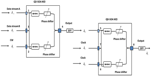
Because the NAND operation is just a series combination of AND and NOT operations, then we can realize the all-optical logic NAND operation using this QD-SOA-MZI scheme as shown in Figure . The first QD-SOA-MZI serves in the system as an optical logic AND gate. After screening out all other wavelength components using a band-pass filter (BPF), the A AND B output data stream (λ2) is amplified to desired power by an amplifier and guided into port 5 as data to one arm of the second MZI for INVERT operation. In this way, the result centered at λ1 coming out of port 8 will be the INVERT of signal injected into port 5, which is the same as logic A NAND B. Based on Figures and , NAND logic gate is the building block of all-optical latches such as Set-Reset and D-Flip-flop. Thus, we can use the QD-SOA-MZI system in Figure to realize all-optical latches.
Figure 15. Schematic of all-optical NAND logic gate based on QD-SOA-MZI.
4.2. Simulation result
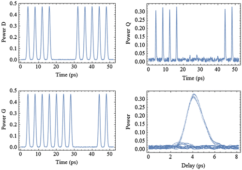
Simulated results of logic gate NAND, Set-Reset latch and D-Flip-Flop are shown in Figures –, respectively (Li, Hu, & Dutta, Citation2013a; Li, Ma, Hu, & Dutta, Citation2012a). The output eye diagram is also plotted to show the output quality. Based on the simulated results in Figures –, it is proved that all-optical Set-Reset latch and D-Flip-Flop operation @ ~250 Gb/s is feasible.
Figure 16. Data A and Data B are shown in the left. Simulated results of output (NAND) and eye pattern of the output are shown in the right.
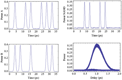
Figure 17. Set and Reset are shown in the left. Simulated results of output (Q) and eye pattern of the output are shown in the right.
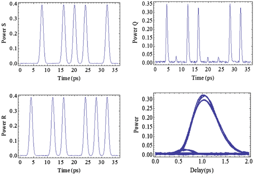
Figure 18. Data and Gate are shown in the left. Simulated results of output (Q) and eye pattern of the output are shown in the right.
5. All-optical encryption and decryption using QD-SOA
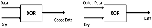
Encryption and decryption has long been used by governments to facilitate secret communication. It is now commonly used in protecting information within many kinds of civilian systems. For example, encryption can be used to protect data being transferred via Internet, mobile telephones, wireless intercom systems and prevent unauthorized use or reproduction of copyrighted material. In an encryption scheme, the message is encrypted using an encryption algorithm. This is usually done with the use of an encryption key, which specifies how the information is to be encoded. An encryption scheme usually needs a key-stream generator to randomly produce keys. The PRBS can be used as the key for encryption and decryption.
The PRBS using linear feedback shift registers (LFSR), which were first introduced in electronics, are characterized by its simplicity of generation, good repeatability, and statistical properties (Golomb, Citation1967). It thus received wide application, including in simulation of noise in signal transmission, data encryption/decryption, and in bit error rate testers (BERT) (Zoiros, Houbavlis, & Kalyvas, Citation2004). The recent achievements in photonics signal processing spurred more interest toward realizing high-speed all-optical PRBS generation. A PRBS can be generated using a linear feedback shift register (LFSR) (Senior, Citation1985). The PRBS sequence generated with a shift register of length m has a period of 2m − 1. To generate a stable all-optical PRBS sequence using LFSR, an optical XOR logic gate is needed. A model to simulate the process of high-speed all-optical encryption and decryption is presented in (Li et al., Citation2013b). The encryption algorithm and the key we used in this model are XOR operation and PRBS. Both of the high-speed all-optical XOR operation and PRBS are realized using the QD-SOA Mach–Zehnder interferometer. Two other kinds of more secure key-stream generators: cascaded design and parallel design were also designed and investigated.
5.1. Schematic of all-optical encryption and decryption
The logic XOR operation can be used to realize the encryption and decryption of the message. The message can be encrypted by applying the bitwise XOR operation to every character using a given key. To decrypt the coded message, we merely reapply the XOR operation with the same key which is used for encryption. The schematic of encryption and decryption using the same key are shown in Figure . The high-speed all-optical logic operations which are used for all-optical encryption and decryption are realized using QD-SOA-MZI as shown in Figure .
Figure 19. The left figure is the schematic of encryption. The right figure is the schematic of decryption.
5.2. Generation of the key
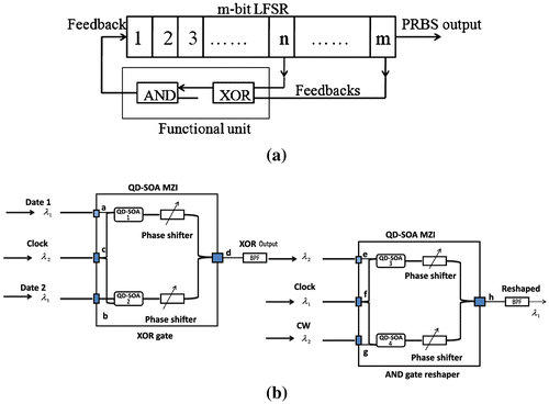
The key used for encryption and decryption is high-speed all-optical PRBS which is generated by a linear feedback shift register (LFSR) composed of QD-SOA-based logic XOR and AND gates, shown in Figure (a). An LFSR has m data storing units (optical delay line in all-optical system), each unit is capable of storing one binary data bit for one clock period (Kalyvas, Yiannopoulos, Houbavlis, & Avramopoulos, Citation2003). The whole system is synchronized with a clock. At each period, the nth and mth bit go through an XOR process (Ma, Li, Hu, & Dutta, Citation2012). Their XOR result gets reshaped and its wavelength is converted back to system’s operation wavelength through an AND gate, and then goes back to the front of LFSR. The output PRBS signals can be tapped from the end of the LFSR. Figure (b) shows the design of the logic functional unit. The main parts of this unit are two Mach–Zehnder interferometers (MZI) each arm of which has a semiconductor optical amplifier (SOA) with a quantum dot (QD) active region. The first MZI serves as an all-optical logic XOR gate for the two bits (m, n), while the other MZI serves as logic AND gate.
Figure 20. Design of PRBS generator. (a): Block diagram of a LFSR (b): functional unit, including two QD-SOA MZIs operating as XOR and AND gates.
The PRBS sequence generated using this scheme has a repetition bit period of T = 2m − 1. Basically, the PRBS sequences are different from truly random bit sequences in that the latter has a continuous spectrum while the former has a discrete spectrum with harmonics (Dutta & Wang, Citation2006). As m increases, the generated PRBS spectrum becomes more and more continuous and the output can better represent a truly random signal. The frequency space between two neighboring lines in the frequency spectrum of PRBS sequences is given by (Dutta & Wang, Citation2006)(15)
(15)
where fb is the bit rate. From the above equation, we can see as m increases the frequency space becomes smaller which means the PRBS frequency spectrum becomes more and more continuous. Thus, as m increases the randomness of PRBS sequence becomes better.
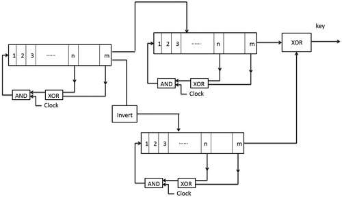
Two other kinds of more secure key-stream generators, cascaded design and parallel design were also presented, shown in Figures and (Akiyama, Wada, et al., Citation2000). The cascaded design consists of three cascaded linear feedback shift registers (LFSR) which can generate all-optical PRBS. The output of the first LFSR can be used as the input of the second LFSR and the output of the second LFSR can be used as the input of the third LFSR. All these three LFSR are realized using the QD-SOA MZIs. The parallel design is composed of three linear feedback shift registers (LFSR), an INVERT gate and a XOR gate. The output of the first LFSR and its invert are used as the input of the second LFSR and the third LFSR, respectively. The final output is the XOR of the output of second LFSR and third LFSR. The three LFSR and all the logic gates are realized using QD-SOA MZIs too.
Figure 21. Block diagram of cascaded designed key-stream generator.
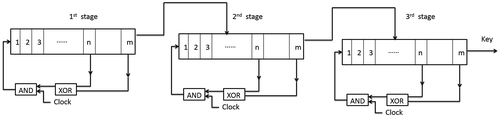
Figure 22. Block diagram of parallel designed key-stream generator.
5.3. Simulation results
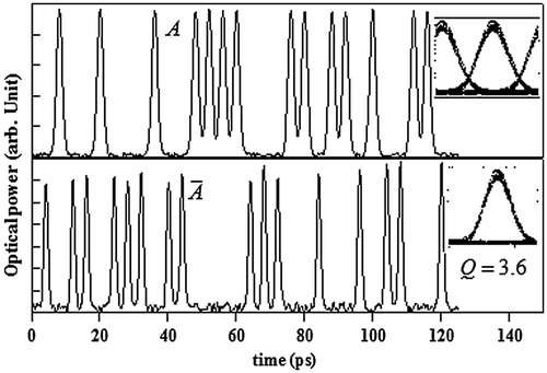
The simulated results of encryption and decryption for the QD-SOA-based XOR operation are shown in Figure (Li et al., Citation2013b). Input data are on the top right and a key (chosen any of bots in this case) is shown on top left. The encrypted in XOR of the input data and key is shown on bottom left. The decrypted data which should be the original data is shown on bottom right. Note that top right and bottom right traces are identical as it should be. Thus, it is proved that all-optical encryption and decryption operation at ~250 Gb/s is feasible. The Q factor was also calculated for the decrypted data in Figure . The Q factor is 8.7, which means a good quality of the decrypted data.
Figure 23. Input data is shown at the top-right corner and key is shown at the top-left corner. Simulated results of encrypted data and decrypted data are shown at the bottom-left corner and bottom-right corner, respectively.
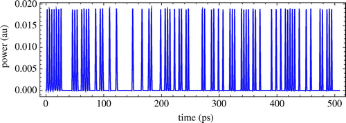
The key used for encryption and decryption is high-speed all-optical PRBS. The all-optical PRBS generated by a 7-bit optical LFSR is simulated by modeling the logic XOR and AND operations based on QD-SOAs as shown in Figure .
Figure 24. Simulation result of PRBS sequences generated by 7-bit LFSR, operating at 250 Gb/s.
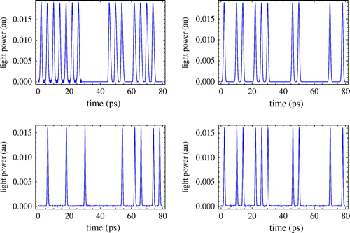
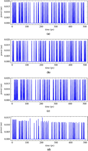
The numerical simulation results of cascaded design and parallel design key-stream generators are shown in Figures and , respectively. As shown in Figures and , the cascaded design and parallel design key-stream generators operating at ~250 Gb/s is feasible. Thus, we can use these two kinds of key-stream generators to produce various more secure keys.
Figure 25. (a) Simulation result of the first stage in cascaded design, input is seven “1”; (b) Simulation result of the second stage in cascaded design, input is “8th–14th” of the output of the first stage; (c) Simulation result of the third stage in cascaded design, input is “15th–21st” of the output of the second stage.
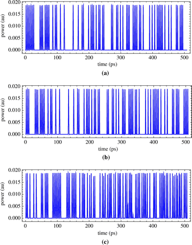
Figure 26. (a) Simulation result of the first LFSR in parallel design, input is seven “1”; (b) Simulation result of the second LFSR in parallel design, input is “8th-14th” of the output of the first LFSR; (c) Simulation result of the third LFSR in parallel design, input is the invert of “8th–14th” of the output of the first LFSR; (d) the final output of parallel design: XOR of the output of second and third LFSR.
6. Summary and perspective
The model to simulate high-speed all-optical logic gates using QD-SOA-based Mach–Zehnder interferometer was presented. Results show that QD-SOA-based MZI can perform logic operations such as AND, XOR, NOT, and NAND at high speed up to 250 Gb/s. The impact on the high-speed output quality (Q-factor), from injected current density, transition lifetime between QD excited state and ground state, pulse width and single pulse energy, are also studied and discussed. The design and simulation of all-optical latches and all-optical encryption using QD-SOA were also presented and investigated. These research results proved that high-speed all-optical logic generation based on QD-SOA-MZI is a feasible and promising method to realize all-optical network in the future. Further investigation on more complex all-optical circuit based on all-optical logic gates is required.
Funding
The authors received no direct funding for this research.
Additional information
Notes on contributors
Hongyu Hu
Hongyu Hu was born in Fuzhou, China, in 1988. He received his BSc from the Harbin Institute of Technology, Harbin, China, in 2011. He completed his PhD in physics from University of Connecticut. His research interests include nonlinear optics, fiber optics communication, and semiconductor lasers.
Xiang Zhang
Xiang Zhang was born in Jiangsu, China, in 1991. He was awarded his Bachelor of Science from Xiamen University, China. He is currently pursuing his PhD at the University of Connecticut. His research interests are in laser optics, fiber optics, and optical communications.
Shuai Zhao
Shuai Zhao was born in Liaoning, China, in 1988. She was awarded her Bachelor of Engineering from Dalian University of Technology, China. She completed her PhD in Chemical Engineering from the University of Connecticut. Her research interests are fuel cell and electrochemistry.
References
- Akiyama, T., Kuwatsuka, H., Simoyama, T., Nakata, Y., Mukai, K., Sugawara, M., … Ishikawa, H. (2000). Application of spectral-hole burning in the inhomogeneously broadened gain of self-assembled quantum dots to a multiwavelength-channel nonlinear optical device. IEEE Photonics Technology Letters, 12(10), 1301–1303.10.1109/68.883810
- Akiyama, T., Wada, O., Kuwatsuka, H., Simoyama, T., Nakata, Y., Mukai, K., … Ishikawa, H. (2000). Nonlinear processes responsible for nondegenerate four-wave mixing in quantum-dot optical amplifiers. Applied Physics Letters, 77(12), 1753.10.1063/1.1311319
- Berg, T., & Mork, J. (2004). Saturation and noise properties of quantum-dot optical amplifiers. IEEE Journal of Quantum Electronics, 40(11), 1527–1539.10.1109/JQE.2004.835114
- Berg, T. W., & Mørk, J. (2003). Quantum dot amplifiers with high output power and low noise. Applied Physics Letters, 82(18), 3083–3085.10.1063/1.1571226
- Bintjas, C., Kalyvas, M., Theophilopoulos, G., Stathopoulos, T., Avramopoulos, H., Occhi, L., … Dall’ Ara, R. (2000). 20 Gb/s all-optical XOR with UNI gate . IEEE Photonics Technology Letters, 12(7), 834–836.10.1109/68.853516
- Chan, K., Chan, C., Chen, L., & Tong, F. (2004). Demonstration of 20 Gb/s all-optical XOR gate by four-wave mixing in semiconductor optical amplifier with RZ-DPSK modulated inputs. IEEE Photonics Technology Letters, 16(3), 897–899.10.1109/LPT.2004.823750
- Diez, S., Schubert, C., Ludwig, R., & Ehrke, H. (2000). 160 Gbit/s all-optical demultiplexer using hybrid gain-transparent SOA Mach–Zehnder interferometer . Electronics Letters, 36(17), 1484–1486.10.1049/el:20001041
- Dong, H., Sun, H., Wang, Q., Dutta, N. K., & Jaques, J. (2006). All-optical logic and operation at 80 Gb/s using semiconductor optical amplifier based on the Mach–Zehnder interferometer. Microwave and Optical Technology Letters, 48(8), 1672–1675.10.1002/(ISSN)1098-2760
- Dorren, H. J. S., Hill, M. T., Liu, Y., Calabretta, N., Srivatsa, A., Huijskens, F. M., … Khoe, G. D. (2003). Optical packet switching and buffering by using all-optical signal processing methods. Journal of Lightwave Technology, 21(1), 2–12.10.1109/JLT.2002.803062
- Dutta, N. K., & Wang, Q. (2006). Semiconductor optical amplifier. Singapore: World Scientific.10.1142/5879
- Golomb, S. W. (1967). Shift register sequences. San Francisco: Holden-Day.
- Houbavlis, T., Zoiros, K., Hatziefremidis, A., Avramopoulos, H., Occhi, L., Guekos, G., … Dall’ Ara, R. (1999). 10 Gbit/s all-optical Boolean XOR with SOA fiber Sagnac gate. Electronics Letters, 35(19), 1650.10.1049/el:19991142
- Hu, H., Zhang, X., Li, W., & Dutta, N. K. (2016). Hybrid mode-locked fiber ring laser using graphene and charcoal nanoparticles as saturable absorbers. SPIE Defense + Security, 983630–983630-8.
- Kalyvas, M., Yiannopoulos, K., Houbavlis, T., & Avramopoulos, H. (2003). Design algorithm of all-optical linear feedback shift registers. AEU - International Journal of Electronics and Communications, 57(5), 328–332.10.1078/1434-8411-54100179
- Kang, I., Dorrer, C., Liming, Z., Dinu, M., Rasras, M., Buhl, L., … Jaques, J. (2008). Characterization of the dynamical processes in all-optical signal processing using semiconductor optical amplifiers. IEEE Journal of Selected Topics in Quantum Electronics, 14(3), 758–769.10.1109/JSTQE.2008.917020
- Kang, I., Dorrer, C., Zhang, L., Rasras, M., Buhl, L., Bhardwaj, A., … Giles, C. R. (2005). Regenerative all optical wavelength conversion of 40-Gb/s DPSK signals using a semiconductor optical amplifier Mach–Zehnder interferometer. In ECOC 2005, paper Th4.3.3.
- Kim, J., Jhon, Y., Byun, Y., Lee, S., Woo, D., & Kim, S. (2002). All-optical XOR gate using semiconductor optical amplifiers without additional input beam. IEEE Photonics Technology Letters, 14(10), 1436–1438.
- Li, W. (2015). High speed all optical switching and encryption using ultrafast devices (Doctoral dissertations). 956. Retrieved from http://digitalcommons.uconn.edu/dissertations/956
- Li, W., Ma, S., Hu, H., & Dutta, N. K. (2012a). All optical latches using quantum-dot semiconductor optical amplifier. Optics Communications, 285(24), 5138–5143.10.1016/j.optcom.2012.07.085
- Li, W., Ma, S., Hu, H., & Dutta, N. K. (2012b). All-optical latches based on two-photon absorption in semiconductor optical amplifiers. Journal of the Optical Society of America B, 29(9), 2603–2609.10.1364/JOSAB.29.002603
- Li, W., Hu, H., & Dutta, N. K. (2013a). Optical latches using optical amplifiers. SPIE Defense, Security, and Sensing, 87200O-1–87200O-9.
- Li, W., Hu, H., & Dutta, N. K. (2013b). High speed all-optical encryption and decryption using quantum dot semiconductor optical amplifiers. Journal of Modern Optics, 60(20), 1741–1749.10.1080/09500340.2013.856486
- Li, W., Hu, H., & Dutta, N. K. (2014). High speed all-optical PRBS generation using binary phase shifted keyed signal based on QD-SOA. SPIE Proceedings, 9202.
- Li, W., Hu, H., Zhang, X., & Dutta, N. K. (2015). High speed all optical logic gates using binary phase shift keyed signal based on QD-SOA. International Journal of High Speed Electronics and Systems, 24(3).
- Li, W., Hu, H., Zhang, X., Zhao, S., Fu, K., & Dutta, N. K. (2016). High-speed ultrashort pulse fiber ring laser using charcoal nanoparticles. Applied Optics, 55(9), 2149.10.1364/AO.55.002149
- Li, Z., Liu, Y., Zhang, S., Ju, H., de Waardt, H., Khoe, G. D., … Lenstra, D. (2005). All-optical logic gates using semiconductor optical amplifier assisted by optical filter. Electronics Letters, 41(25), 1397.10.1049/el:20053385
- Ma, S., Chen, Z., Sun, H., & Dutta, N. K. (2010). High speed all optical logic gates based on quantum dot semiconductor optical amplifiers. Optics Express, 18(7), 6417–6422.10.1364/OE.18.006417
- Ma, S., Li, W., Hu, H., & Dutta, N. K. (2012). Optical processors using semiconductor optical amplifiers. SPIE Defense, Security, and Sensing, 840303–840303-4.
- Mukai, K., Nakata, Y., Shoji, H., Sugawara, M., Ohtsubo, K., Yokoyama, N., & Ishikawa, H. (1998). Lasing with low threshold current and high output power from columnar-shaped InAs/GaAs quantum dots. Electronics Letters, 34(16), 1588.10.1049/el:19981075
- Reithmaier, P., & Eisenstein, G. (2008). Semiconductor optical amplifiers with nanostructured gain material. In Frontiers in Optics, OSA Technical Digest (CD) (Optical Society of America, 2008), paper FTuN1.
- Ridha, P., Li, L., Rossetti, M., Patriarche, G., & Fiore, A. (2008). Polarization dependence of electroluminescence from closely-stacked and columnar quantum dots. Optical and Quantum Electronics, 40(2–4), 239–248.10.1007/s11082-007-9173-6
- Senior, J. M. (1985). Optical fibre communications – Principles and practice. London: Prentice-Hall.
- Wang, Q., Zhu, G., Chen, H., Jaques, J., Leuthold, J., Piccirilli, A. B., & Dutta, N. K. (2004). Study of all-optical XOR using Mach–Zehnder interferometer and differential scheme. IEEE Journal of Quantum Electronics, 40(6), 703–710.10.1109/JQE.2004.828261
- Zhang, X., Hu, H., Li, W., & Dutta, N. K. (2016). High-repetition-rate ultrashort pulsed fiber ring laser using hybrid mode locking. Applied Optics, 55(28), 7885–7891.10.1364/AO.55.007885
- Zhang, X., Li, W., Hu, H., & Dutta, N. K. (2015a). Two-photon absorption-based optical logic. SPIE Defense + Security, 946731–946731-10.
- Webb, R., Manning, R., Maxwell, G., & Poustie, A. (2003). 40 Gbit∕s all-optical XOR gate based on hybrid-integrated Mach–Zehnder interferometer . Electronics Letters, 39(1), 79–81.10.1049/el:20030010
- Zhang, X., Li, W., Hu, H., & Dutta, N. K. (2015b). High speed all-optical encryption and decryption based on two-photon absorption in semiconductor optical amplifiers. Journal of Optical Communications and Networking, 7(4), 276–285.
- Zoiros, K. E., Houbavlis, T., & Kalyvas, M. (2004). Ultra-high speed all-optical shift registers and their applications in OTDM networks. Optical and Quantum Electronics, 36(11), 1005–1053.10.1007/s11082-004-2040-9