
Abstract
The objective of this study was to demonstrate the possibility of using 1-butanol to reliably detect the open-pore current of pyramidal solid-state nanopores produced in silicon wafers. The nanopores were produced through controlled pore formation by neutralizing an etchant (KOH) with a strong acid (HCl). Since nanopores produced by this method are deeper than those made in nanometer-thick membranes, they behave as nanochannels. As a consequence, the open-pore current detection is more challenging. Thus, we report that low amounts of butanol considerably aid in the detection of the open-pore current of nanopores.
Public Interest Statement
In this paper, the nanopores were produced through controlled pore formation by neutralizing an etchant with a strong acid. We report that low amounts of butanol considerably aid in the detection of the open-pore current and help stabilize the current signal.
1. Introduction
Nanopore-based technologies are emerging as powerful tools for single molecule analysis. At present, the production of solid-state nanopores in silicon nitride/dioxide membranes (SiO2/Si3N4) has generated great interest because of potential application such as detection of single-stranded DNA (Chang et al., Citation2004; Iqbal, Akin, & Bashir, Citation2007; Zwolak & Di Ventra, Citation2005), double-stranded DNA (Kwok, Briggs, & Tabard-Cossa, Citation2014; Rodríguez-Manzo, Puster, Nicolaï, Meunier, & Drndić, Citation2015; Yanagi, Akahori, Hatano, & Takeda, Citation2014), and proteins (Fologea, Ledden, McNabb, & Li, Citation2007; Yu et al., Citation2015; Yusko et al., Citation2011). The conventional method for the production of such nanopores involves the use of microscopic equipment such as Focused Ion Beam (Ayub et al., Citation2010; Gadgil, Tong, Cesa, & Bennink, Citation2009; Mussi et al., Citation2010; Stein, McMullan, Li, & Golovchenko, Citation2004) or Transmission Electron Microscopy (Fologea, Uplinger, Thomas, McNabb, & Li, Citation2005; Storm, Chen, Ling, Zandbergen, & Dekker, Citation2003). This type of equipment is expensive, has low throughput, and in many cases it might be difficult to access, limiting the commercial production of solid-state nanopores by these methods. In recent years, several research groups have developed techniques which are easier to reproduce and do not require the use of expensive equipment. Among them are dielectric breakdown (Kwok et al., Citation2014), pulse-voltage injection methods (Yanagi et al., Citation2014), or electrochemical etching combined with an electric control of pore formation (Park, Peng, & Ling, Citation2007). However, these methods require human intervention or an automation method to stop the etching reaction. Additionally, manipulation and washing of thin membranes is challenging because they are fragile and break easily. Therefore, it is necessary to have a reproducible manufacturing method which does not require expensive equipment and is easy to implement at low production costs. We propose an automated and inexpensive method for the production of solid state nanopores in silicon wafers. The fabrication process involves wet silicon etching with potassium hydroxide (KOH) and controlled opening of a nanopore by chemical braking with hydrochloric acid (HCl) in a subsequent step. The depth of nanopore obtained by this method is considerably higher than nanopores made in nanometer-thick membranes.
Due to the lithographic process and the thickness of the silicon wafer used, a pyramidal structure is obtained, where the depth of the pyramid is 200 μm thick. This structure makes these nanopores stiffer than those nanopores made in membranes. However, due to the large depth of the pyramid, bubble formation is favored which could affect the pore resistance. This is an important parameter because it can be associated with the pore size. Thus, as the pore size is smaller, the resistance is higher. If the size is previously known, this value could indicate blockage in the pore, which can be confirmed through the presence of bubbles in the buffer, very common in this type of procedure. To properly determine the resistance or conductance of the pore, the I-V measurements were performed with both sides of the silicon wafer in contact with salt buffer and using Ag/AgCl wires as electrodes (Park et al., Citation2007).
In this paper, the effect of 1-butanol for removing bubbles generated in the buffer due to the depth of the nanopore was studied.
Butanol is a primary alcohol, consisting of four carbons with the formula C4H10O. Because of the four carbons in the alcohol chain, its solubility in water decreases rapidly as the polar hydroxyl group (-OH) is relatively small compared to the hydrocarbon portion (Lee et al., Citation2008). Additionally, the 1-butanol used in this study has great ability to reduce the water interfacial tension (Chen, Siepmann, & Klein, Citation2002). Furthermore, butanol was chosen instead of ethanol, because the dissociation constant of butanol is two orders of magnitude smaller (Müller-plathe, Citation1996). Therefore, butanol is less acidic, because it is a long chain alcohol, allowing the bubbles to dissolve.
2. Methods
2.1. Pattern formation and first chemical etching
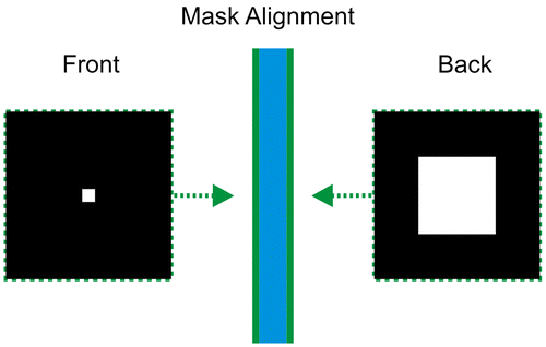
The substrates used were 700 μm thick double-side polished <100> oriented silicon wafers (Virginia Semiconductor In). A silicon nitride layer of 50 nm thickness was grown on a wafer using plasma enhanced chemical vapor deposition (PECVD) at 600°C. The gas used for plasma deposition was hexamethyldisilazane (CH3)3SiNHSi(CH3)3 and nitrogen as reactive gas. Square shapes in both sides of the wafer were defined by photolithography using AZ9260 photoresist (Figure ). The photoresist was spinned on the silicon wafers at 2,400 rpm, then a pre-heating step was conducted for 3 min at 110°C. The photoresist was exposed for 40 s using an EVG 620 mask aligner (300 W UV Plane focus light of 6 in diameter), and developed using AZ 400 developer: DI water 1:4. Subsequently reactive ion etching (RIE) was performed. Thus, it was possible to remove the Si3N4 layer, exposing the square shapes previously defined on the silicon wafer. The RIE (Reactive Ion Etching) process for the Si3N4 passivation layer was carried out in a plasma etching equipment (Plasma lab 80, Oxford). The wafer was placed on a quartz cover plate to avoid sputtering/redeposition of electrode material and gas was injected into process chamber via showerhead gas inlet in the top electrode. Negative self-bias forms on lower electrode and a single RF plasma source determine both ion density and energy. For our experiments, the RF power applied was 13.6 MHz, and the chamber pressure. Subsequently the remaining photoresist was removed with acetone.
Figure 1. Mask design for both sides of the silicon wafer. The front and back squares have 210 μm and 2.1 mm, respectively.
The first etching was performed simultaneously on both sides of the silicon wafer using 7 M KOH at 80°C for 360 min. The reaction was stopped before the inverted pyramids joined. The silicon wafer was then removed from the container in which the first etching was performed.
2.2. Second chemical etching (chemical braking)
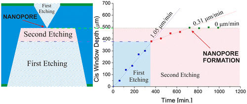
Subsequently, the wafer was placed on a polydimethylsiloxane device between two isolated compartments for carrying out a second etching at 60°C for 630 min with 4 M KOH on one side (cis), while the opposite side was exposed to 12 M HCl (trans). An electric potential of 3 V was applied via platinum electrodes between the two compartments, acting as a driving force for the passage of protons to the trans side and thus accelerating the chemical braking for the controlled nanopore formation (Vega, Lerner, Lasorsa, Pierpauli, & Perez, Citation2016). The inverted pyramid exposed to KOH continues to grow until it meets the other inverted pyramid from the opposite side.
The window depth was measured every 90 min on the cis side (Figure ), and after 750 min it was observed that the depth of the window remained constant, indicating that the etching process was over. In fact, even after 1,000 min no further increase was observed, confirming that the etching reaction had stopped due to the chemical braking.
Figure 2. Rate of nanopore formation using 4 M (KOH) at 60°C and 3 V.
After the second etching, the silicon wafers were immersed in warm DI water (32°C) for 32 h to remove any salt residues, produced in the chemical neutralization process. The samples were oxidized at 800°C with an oxygen flow of 0.5 l min−1 for 30 min in order to fine-tune the pore size and reduce the noise. The thickness of the silicon dioxide layer obtained was approximately 25 nm around the nanopore.
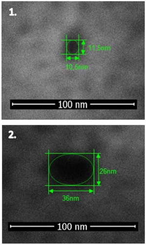
Nanopores of approximately 10 and 35 nm with and without passivation layer were selected to be used in butanol and salt assays. The size of the nanopores was confirmed by scanning electron microscopy (SEM) (Figure ).
Figure 3. SEM images of solid state nanopore after SiO2 deposition.
3. Results and discussion
3.1. Open-pore current detection using butanol
To determine the open-pore current, conductance measurements were carried out on both sides of the silicon wafer. For that, 1 M [KCl] solution was used, with Ag/AgCl electrodes and an Axopatch 200 B device as current amplifier set at 10 kHz sampling rate, and an internal low-pass Bessel filter set at 2 kHz.
To check the behavior and signal stability, the open-pore current was measured in nanopores of similar size (10 and 35 nm) with and without SiO2 insulating layer. Tests were made using buffer KCl Tris 50 mM-HCl pH 7.5 at two different KCl concentrations (0.5 M and 1 M), because they are the most commonly used in biomolecule detection with solid-state nanopores (Chapman, Fee, & Maroncelli, Citation1995; Mussi et al., Citation2009; Wanunu, Sutin, McNally, Chow, & Meller, Citation2008).
The open-pore current signal was unstable after a few minutes for nanopores without SiO2 insulating layer, while for nanopores coated with SiO2 insulating layer it was more stable. It was possible to determine the pore resistance at 90 mV, the results are shown in Figure .
Figure 4. Salt effect concentration on nanopores of two different diameters with and without insulation layer.
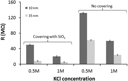
According to Figure , it was possible to establish that: (i) the resistance is higher at low salt concentration. This is similar to that reported by Smeets et al. (Citation2006) for nanopores made in silicon nitride membrane where the ionic conductance also decreased by decreasing the salt concentration. (ii) The resistance values were higher for nanopores without insulation layer. Also, as mentioned above, the generated signal was noisy, unstable, and the pore was finally blocked in about 3 min. The probability of bubble formation is greater in this kind of nanopores, affecting current measurement and finally generating the pore blocking. (iii) The resistance was higher in the 10 nm nanopore with respect to the 35 nm one.
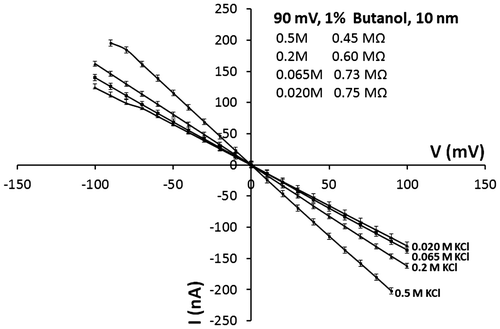
Figure 5. Open-pore current of a 10 nm pore with butanol (1%) at different salt concentrations.
For this reason, the effect of butanol to improve and stabilize the open-pore current was tested. When protons are in excess, because of the high salt concentration, aprotic polar solvents such 1-butanol can form hydrogen bonds (Mussi et al., Citation2009) which can increase and stabilize the current signal. To validate this assumption, different concentrations of KCl and butanol were tested to study the effect on the open-pore current.
3.2. Effect of salt concentration
The experiments were conducted using KCl. To detect the open-pore current, the buffer was supplemented with 1% butanol and voltages up to 100 mV at different salt concentrations (0.02 M, 0.065 M, 0.2 M, 0.5 M KCl) were studied. The results for the 10 nm nanopore are shown in Figure (similar behavior was observed for a 35 nm diameter nanopore).
No significant difference in pore resistance could be observed between 0.020 M and 0.065 M KCl, while 0.2 M to 0.5 M KCl significantly decreased pore resistance. This may be beneficial for sensing biomolecules because in some cases partial pore blockage is generated due to the presence of bubbles or translocation of biomolecules such as DNA through the pore. Smeets et al. (Citation2006) report a gradual decrease in conductance as the potassium chloride concentration is lowered. So the detected current may not be the real signal, for this reason the measurement of DNA studies are usually made between 0.5 and 1 M salt concentration. This is because it improves mobility of DNA through the pore (Keyser et al., Citation2006).
In a 10-nm pore coated with insulating layer, at 0.5 M KCl, the resistance decreases from 61 to 0.45 MΩ when butanol is added. Without insulation layer, the decrease is still more pronounced when butanol is added (from 131 to 0.45 MΩ). This behavior is because butanol helps to remove bubbles generated inside the nanopore. Additionally, in both cases, the addition of butanol shows a stabilization of the current signal for a long period of time (50 min).
3.3. Effect of butanol concentration
In order to determine if the concentration of butanol influences the behavior of the open-pore current, various percentages of butanol in a 0.5 M KCl buffer were studied. As shown in Figure , there is correlation between butanol concentrations and pore resistance. Notably, using 0.5 and 1% butanol, a stable open-pore current could be observed for approximately 50 min. The resistance increases as the percentage of butanol decreases. This behavior may be because at concentrations below 0.5% butanol is insufficient to eliminate bubbles generated inside the nanopore. Additionally, at concentrations lower than 0.5% butanol, the current signal stability was progressively lowered. According to the above, it was established that the optimum conditions are 0.5 M salt concentration and 0.5% butanol.
Figure 6. Open-pore current of a 10 nm pore using the same salt concentration (0.5 M) and varying butanol concentrations.
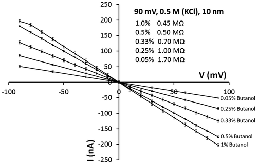
The resistance for a 35 nm nanopore was also determined using 0.5 M KCl and 0.5% butanol at 90 mV, obtaining a value of 0.45 MΩ, which it was a slightly lower value to the resistance of the 10 nm nanopore (0.5 MΩ), as it was expected.
4. Conclusions
We demonstrated that the addition of low concentrations of butanol in the working buffer (1% or less) improves the open-pore current detection and helps to stabilize the current signal.
Butanol eliminates the bubbles generated inside the pore which significantly affect the current measurement, regardless of the pore diameter used, and still maintain the tendency that with a smaller pore diameter, the resistance is higher.
The addition of butanol decreases the resistance of the nanopores regardless of the presence of a passivation layer. At a fixed KCl concentration, increasing the concentration of butanol decreases the resistance of the nanopores.
In summary, butanol was shown to improve current measurements by eliminating bubbles in pyramidal nanopores. Given its properties, it is suggested as a good candidate for use in all types of nanopores.
Funding
This work was supported by CONICET-YPF [PIO-2014]; ANPCyT [PICT2012-575/PICT2013- 0840]; FAN 2014, Argentina.
Cover image
Source: Author
Acknowledgments
The authors thank to Itzel Santizo and J. L. Fernandez for technical support and discussion.
Additional information
Notes on contributors
B. Lerner
Lerner Betiana has wide experience in the development of nanopore devices for more than 10 years.
During this time, she has implemented various nanopore manufacturing methods, such as electrochemical method, laser ablation, optical method, and finally the chemical method. This method has several advantages over the techniques found in literature, as for example: reduction in the processing times, reduction in manufacturing steps, does not require extremely expensive equipment, the manufacturing process stops automatically when the nanopores are formed, and allows scaling.
The research group is also specialized in the design and fabrication of microfluidic devices.
References
- Ayub, M., Ivanov, A., Instuli, E., Cecchini, M., Chansin, G., McGilvery, C., … Albrecht, T. (2010). Nanopore/electrode structures for single-molecule biosensing. Electrochimica Acta, 55, 8237–8243.
- Chang, H., Kosari, F., Andreadakis, G., Alam, M., Vasmatzis, G., & Bashir, R. (2004). DNA-Mediated fluctuations in ionic current through silicon oxide nanopore channels. Nano Letters, 4, 1551–1556.10.1021/nl049267c
- Chapman, C., Fee, R., & Maroncelli, M. (1995). Measurements of the solute dependence of solvation dynamics in 1-propanol: The role of specific hydrogen-bonding interactions. The Journal of Physical Chemistry, 99, 4811–4819.10.1021/j100013a060
- Chen, B., Siepmann, J. I., & Klein, M. L. (2002). Vapor−Liquid interfacial properties of mutually saturated water/1-butanol solutions. Journal of the American Chemical Society, 124, 12232–12237.10.1021/ja027130n
- Fologea, D., Uplinger, J., Thomas, B., McNabb, D. S., & Li, J. (2005). Slowing DNA translocation in a solid-state nanopore. Nano Letters, 5, 1734–1737.10.1021/nl051063o
- Fologea, D., Ledden, B., McNabb, D. S., & Li, J. (2007). Electrical characterization of protein molecules by a solid-state nanopore. Applied Physics Letters, 91, 053901.10.1063/1.2767206
- Gadgil, V., Tong, H., Cesa, Y., & Bennink, M. (2009). Fabrication of nano structures in thin membranes with focused ion beam technology. Surface and Coatings Technology, 203, 2436–2441.10.1016/j.surfcoat.2009.02.036
- Iqbal, S. M., Akin, D., & Bashir, R. (2007). Solid-state nanopore channels with DNA selectivity. Nature Nanotechnology, 2, 243–248.10.1038/nnano.2007.78
- Keyser, U. F., Koeleman, B. N., van Dorp, S., Krapf, D., Smeets, R. M. M., Lemay, S. G., ... Dekker, C. (2006). Direct force measurements on DNA in a solid-state nanopore. Nature Physics, 2, 473–477.10.1038/nphys344
- Kwok, H., Briggs, K., & Tabard-Cossa, V. (2014). Nanopore fabrication by controlled dielectric breakdown. PLoS ONE, 9, e92880.10.1371/journal.pone.0092880
- Lee, S. Y., Park, J. H., Jang, S. H., Nielsen, L. K., Kim, J., & Jung, K. S. (2008). Fermentative butanol production by clostridia. Biotechnology and Bioengineering, 101, 209–228.10.1002/bit.v101:2
- Müller-plathe, F. (1996). An All-Atom Force Field for Liquid Ethanol-Properties of Ethanol-Water Mixtures. Molecular Simulation, 18, 133–143.10.1080/08927029608022358
- Mussi, V., Fanzio, P., Repetto, L., Firpo, G., Valbusa, U., Scaruffi, P., ... Tonini, G. P. (2009). Solid state nanopores for gene expression profiling. Superlattices and Microstructures, 46, 59–63.10.1016/j.spmi.2008.09.003
- Mussi, V., Fanzio, P., Repetto, L., Firpo, G., Scaruffi, P., Stigliani, S., … Valbusa, U. (2010). Electrical characterization of DNA-functionalized solid state nanopores for bio-sensing. Journal of Physics: Condensed Matter, 22, 454104.
- Park, S. R., Peng, H., & Ling, X. S. (2007). Fabrication of nanopores in silicon chips using feedback chemical etching. Small, 3, 116–119.10.1002/(ISSN)1613-6829
- Rodríguez-Manzo, J. A., Puster, M., Nicolaï, A., Meunier, V., & Drndić, M. (2015). DNA translocation in nanometer thick silicon nanopores. ACS Nano, 9, 6555–6564.10.1021/acsnano.5b02531
- Smeets, R. M., Keyser, U. F., Krapf, D., Wu, M.-Y., Dekker, N. H., & Dekker, C. (2006). Salt dependence of ion transport and DNA translocation through solid-state nanopores. Nano Letters, 6, 89–95.10.1021/nl052107w
- Stein, D. M., McMullan, C. J., Li, J., & Golovchenko, J. A. (2004). Feedback-controlled ion beam sculpting apparatus. Review of Scientific Instruments, 75, 900–905.10.1063/1.1666986
- Storm, A., Chen, J., Ling, X., Zandbergen, H., & Dekker, C. (2003). Fabrication of solid-state nanopores with single-nanometre precision. Nature Materials, 2, 537–540.10.1038/nmat941
- Vega, M., Lerner, B., Lasorsa, C. A., Pierpauli, K., & Perez, M. S. (2016). Automated and low cost method to manufacture addressable solid-state nanopores. Microsystem Technologies, 22, 109–117.10.1007/s00542-014-2399-x
- Wanunu, M., Sutin, J., McNally, B., Chow, A., & Meller, A. (2008). DNA translocation governed by interactions with solid-state nanopores. Biophysical Journal, 95, 4716–4725.10.1529/biophysj.108.140475
- Yanagi, I., Akahori, R., Hatano, T., & Takeda, K.-i. (2014). Fabricating nanopores with diameters of sub-1 nm to 3 nm using multilevel pulse-voltage injection. Scientific Reports, 4, 1–7.
- Yu, J.-S., Lim, M.-C., Huynh, D. T. N., Kim, H.-J., Kim, H.-M., Kim, Y.-R., & Kim, K.-B. (2015). Identifying the location of a single protein along the DNA Strand Using Solid-State Nanopores. ACS Nano, 9, 5289–5298.10.1021/acsnano.5b00784
- Yusko, E. C., Johnson, J. M., Majd, S., Prangkio, P., Rollings, R. C., LI, J., ... Mayer, M. (2011). Controlling protein translocation through nanopores with bio-inspired fluid walls. Nature Nanotechnology, 6, 253–260.10.1038/nnano.2011.12
- Zwolak, M., & Di Ventra, M. (2005). Electronic signature of DNA nucleotides via transverse transport. Nano Letters, 5, 421–424.10.1021/nl048289w