
Abstract
Phase change materials are a technologically important materials class and are used for data storage in rewritable DVDs and in phase change random access memory. Furthermore, new applications for phase change materials are emerging. Phase change materials with a high structural quality, such as offered by epitaxial films, are needed in order to study the fundamental properties of phase change materials and to improve our understanding of this materials class. Here, we review the progress made in the growth of crystalline phase change materials by physical methods, such as molecular beam epitaxy, sputtering, and pulsed laser deposition. First, we discuss the difference and similarities between these physical deposition methods and the crystal structures of Ge2Sb2Te5, the prototype phase change material. Next, we focus on the growth of epitiaxial GST films on (0 0 1)- and (1 1 1)-oriented substrates, leading to the conclusion that (1 1 1)-oriented substrates are preferred for the growth of phase change materials. Finally, the growth of GeTe/Sb2Te3 superlattices on amorphous and single crystalline substrates is discussed.
1. Introduction
The wide spread use of phase change materials (PCM), such as GeTe-Sb2Te3 (GST) alloys, makes this material class technologically very relevant [Citation1]. There are two mature main application areas for PCM. The first deals with their use in optical disks for data storage that relies on the optical contrast between the crystalline and amorphous phase of PCM in order to encode digital bits [Citation2]. The second application area is in electronics and is known as phase change random access memory (PRAM) [Citation3,4]. These memory elements exploit the resistance contrast between the amorphous and crystalline phases of PCM. Both applications have in common that they use heat, generated by laser pulses or by Joule heating, in order to switch reversibly between the two phases. Recent years have seen a number of new possible application areas for PCM, ranging from optical displays [Citation5] and photonic memory elements [Citation6] to neuromorphic computing [Citation3,7,8]. More details about the applications of phase change materials can be found in recent review articles [Citation3,8,9].
Great advances have been made in understanding the fundamental properties of PCM by studying amorphous and polycrystalline films. For example, the difference in bonding character between crystalline and amorphous PCM has been identified as the reason for the difference in the optical contrast [Citation10,11]. In addition, crystallization studies have shed light on the fragility of PCM and its influence on the crystallization speed [Citation12,13]. Furthermore, indications for photoassisted amorphization have been found, suggesting that melting is not a prerequisite for amorphization [Citation14,15]. The discussion of the origin of the switching mechanism from the crystalline to amorphous phase is thus still ongoing [Citation16,17]. Moreover, the answer to some questions, such as the determination of the band structure, requires the use of very advanced characterization techniques, such as angle resolved photoemission spectroscopy, that are limited to single crystals or epitaxial thin films.
In recognition of this need, the epitaxial growth of PCM was pioneered using molecular beam epitaxy (MBE) [Citation18]. This made it possible to make initial studies of the band structure of GST [Citation19]. Recent years have seen an increased activity in the growth of epitaxial phase change materials. Besides, MBE epitaxial PCM have now also been grown by pulsed laser deposition (PLD) [Citation20–23], sputtering [Citation24], and metal–organic vapor phase epitaxy (MOVPE) [Citation25,26]. In addition, there is an increased interest in the use of textured PCM due to the enhanced performance of textured GeTe/Sb2Te3 superlattices in PRAM [Citation27]. Given this interest, we think it is the appropriate time to review the growth of epitaxial and textured PCM. Given the fact that the growth of PCM by chemical means has been reviewed recently [Citation28], we restricted ourselves to the growth of PCM by physical means.
This review is organized as follows. First, we discuss the crystal structure of GST alloys. Afterwards, we briefly touch upon the difference between the growth techniques used for the fabrication of crystalline epitaxial PCM. Next, we discuss the growth of epitaxial PCM and look at the influence of the substrate material, as well as substrate orientation. Finally, we review the growth of GST superlattices and textured layers before we end with the conclusions.
2. Crystal structure of GeTe-Sb2Te3 alloys
Ge2Sb2Te5 (GST225) is a prototype phase change material and the growth of PCM has thus focused on this specific alloy. We will discuss the crystal structure of this alloy in the following because the crystal structure is important to epitaxial growth. Crystalline GST has two metastable phases and one stable phase, as shown in the schematic in Figure . GST alloys obey Ostwald’s step rule [Citation29], which states that a crystal first nucleates in the least stable polymorph and subsequently evolves into more stable polymorph before reaching its stable phase. The cubic phase of GST (Figure (a)) is the most unstable crystalline form of GST. It has a lattice constant of 6.0293 Å at room temperature and the NaCl crystal structure, space group [Citation30]. The Te atoms occupy the Cl positions, whereas the Na positions are occupied by Ge and Sb. The occupancy of the Ge/Sb sublattice is however approximately 80%, indicating that there is a large fraction of vacancies (v) present on this sublattice. The random occupation of vacancies is however energetically unstable and the vacancies will form vacancy layers [Citation31]. Thus, upon annealing, the vacancies will order and form vacancy layers on the {1 1 1} planes. Figure (b) shows a GST225 alloy with a completely ordered vacancy layer, which represents the second metastable phase of GST. In reality, films with ordered vacancy layers do not have a perfect ordering of the vacancy layers and the distance between the Te-v-Te planes is about 3.3 Å indicating the presence of some Ge/Sb atoms within the intermediate plane [Citation32]. Furthermore, two successive vacancy layers can be separated by 7, 9, or 11 atomic layers, corresponding to separations of 14, 17, and 21 Å, respectively. This is indicative of a compositional variation [Citation32,33]. In fact, it has to be noted that for GST124, 225 and 326 between two successive vacancy layers 7, 9, and 11 layers are expected, respectively [Citation33]. The vacancy ordered phase is not only characterized by an ordering of vacancies, but also by an ordering Ge and Sb atoms. Specifically, the Sb atoms move closer to the vacancy layer [Citation32].
Figure 1. Schematics (made using VESTA 3[Citation66]) of the metastable and stable crystalline phases of GST. Continuous blue lines represent the unit cell, dashed lines across the Te-ν-Te planes are guide to the eyes for the identification of the cubic and rhombohedral stacking within the cubic ordered and the trigonal phase, respectively.
![Figure 1. Schematics (made using VESTA 3[Citation66]) of the metastable and stable crystalline phases of GST. Continuous blue lines represent the unit cell, dashed lines across the Te-ν-Te planes are guide to the eyes for the identification of the cubic and rhombohedral stacking within the cubic ordered and the trigonal phase, respectively.](/cms/asset/165d3c16-91f7-4fed-9ae3-b8a021dcb2e2/tapx_a_1346483_f0001_oc.gif)
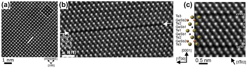
It should be noted that the transition between the two metastable phases is not abrupt, but rather gradual. Atomic imaging of the vacancy ordering process upon annealing of cubic GST exemplarily demonstrated the tendency of vacancies to rearrange from random site within the cation lattice into first patches and subsequently layers ordered along the [1 1 1] directions, thus, demonstrating that the atomic vacancies segregate onto {1 1 1} planes [Citation34]. Such ordering transition can be characterized by an order parameter that is 0 for the first metastable phase and 1 for a fully vacancy ordered phase. A fully ordered vacancy layer will collapse, which will result in the formation of the stable trigonal phase. This transition involves a vertical and horizontal movement of the layers in the lattice. As a result, the atomic columns in the trigonal phase are no longer parallel to each other as shown in Figure (c) by dashed blue lines. The stable phase of GST is very similar to the stable phase of its parent compound Sb2Te3 and is characterized by the presence of van der Waals (vdW) gaps (the collapsed vacancy layers). The symmetry is and the lattice constants are 4.2247 and 17.2391 Å [Citation30]. Initially, it was assumed that the Ge and Sb sublattices in the stable phase were completely ordered and either formed the Petrov [Citation35] or Kooi [Citation36] stacking. However, Matsunaga et al. showed that there is still disorder present in this sublattice and determined that the central layers are for 56 (44)% occupied by Ge (Sb) and layers at the edge for 44 (56)% by Ge (Sb) [Citation30]. Recent scanning transmission electron microscopy investigations have confirmed the existence of these three different phases of GST, as shown in Figure (a)–(c), for the cubic, vacancy ordered and stable phases, respectively. In general, it should be noted that the different phases can exist side by side in a single sample, as is for example observed in MBE epitaxial films [Citation33]. Moreover, the presence of disorder on the Ge/Sb sublattice on the local scale has been confirmed using transmission electron microscopy [Citation20,37].
Figure 2. Real space structural image of the crystalline phases of GST as obtained by transmission electron microscopy.
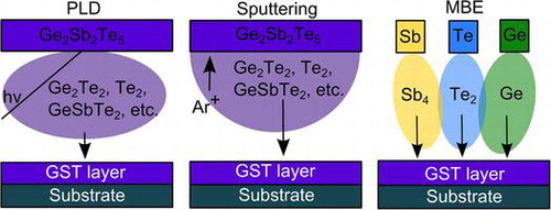
3. Physical deposition methods
The physical deposition methods that have been used to deposit crystalline PCM differ in some aspects that we will discuss here. Figure shows schematic of three different deposition methods used for the fabrication of PCM thin films. In PLD and sputtering, a target with the correct GST composition is typically situated opposite from a heatable substrate holder inside a vacuum chamber. In sputtering, ionized Ar+ atoms are accelerated by an electric field toward the target. Above a critical energy, atomic species are kicked out of the target, i.e. sputtered. These atoms and atom clusters are subsequently deposited on the substrate. In PLD, an intense nanoseconds long UV laser pulse is used to ablate material from the target. Laser Desorption Ionization Time-of-Flight Mass Spectrometry has been used to study the types of clusters that are formed during pulsed laser deposition of GST. It has been shown that the plasma consists of Ge, Ge2, GeTe, Ge2Te, Te, Te2, Te3, GeTe2, Ge2Te2, GeTe3, SbTe2, Sb2Te, GeSbTe2, Sb3Te, and GeSbTe3 [Citation38]. It should be noted that larger clusters might also be present, but could lie outside the detection range of the mass spectrometer. We assume that the plasma in sputtering might consist of similar molecules. Finally, it should be noted that PLD of PCM is typically performed in an Ar background pressure of approximately 0.04 mbar and typical growth rates range from 5 to 40 nm/min [Citation21,22].
Figure 3. Schematics of the different physical deposition methods used for growing epitaxial GST.
In MBE, an ultra-high vacuum (UHV) chamber (<10−9 mbar) is used and the constituents of GST are supplied from independent heatable sources. This makes it possible to control the composition of the growing layer in great extent. Using separate elemental source for each atomic component of the alloy, the elements that arrive at the surface are Ge atoms, Te2, and Sb4 molecules (Sb4 molecules can also be cracked into Sb2 and Sb). Generally, Te2 is supplied in over pressure and the composition is controlled by varying the Ge/Sb4 flux ratio. The typical growth rate is below 1 nm/min. Based on these observations, we can identify a number of differences between these deposition techniques. First, the use of a UHV chamber for MBE implies that the cleanliness of the sample is greater in MBE-grown samples because the background contamination is lower. This is for example important when working with semiconducting substrates, such as silicon. Furthermore, the UHV environment makes it possible to use reflection high energy electron diffraction (RHEED) and line of sight quadrupole mass spectroscopy (QMS) during the deposition. Such techniques can give valuable information about the growth process. Using a differential pumping system it is also possible to use RHEED in PLD [Citation39] or sputtering systems [Citation40]. It should be noted that RHEED is well established for PLD, but not for sputtering. Recently, RHEED has been used to study the growth of Sb2Te3 grown by PLD [Citation41], indicating that it can also be used for other GST compositions during PLD. Finally, the possibility to use separated sources for the constituents in MBE instead of a single compound target as in PLD or sputtering leads to different growth kinetics. In MBE, the molecules react first on the surface, whereas in the other deposition methods, clusters of GST are already present in the vapor phase. In addition, the species that arrive on the substrate surface by means of sputtering or PLD have a much higher energy or are ionized, which influences the deposition [Citation42]. Instead, the energy of molecules that arrives on the surface in MBE is given by the temperature of the effusion cells. The growth using MBE thus occurs closer to thermal equilibrium than the growth using sputtering or PLD. Finally, it has been demonstrated that PCM devices with GST deposited by MBE are comparable with industry standards [Citation43] indicating that MBE can be applied for device fabrication as well.
4. Epitaxial growth of GST
The first demonstration of the epitaxial growth of GST was done by MBE [Citation18]. Recently, the epitaxial growth of GST has also been demonstrated by PLD [Citation22]. The initial aim was to grow the metastable phase of GST. Since the effect of vacancy ordering was unknown at that time, initially, (0 0 1)-oriented GaSb substrates were used as it was expected that GST can be easily grown cube on cube on this substrate. GaSb was chosen as a substrate because it has a low lattice mismatch with cubic GST. Subsequent studies have however shown that (1 1 1)-oriented substrates are more suitable for the growth of GST [Citation44,45], as will be discussed in detail below. It turns out that there indeed is a large difference between the growth on (0 0 1)- and (1 1 1)-oriented substrates that can be attributed to the presence of ordered vacancies in the metastable form of GST. Hence, we will discuss the growth on these two orientations separately. We will focus on the growth dynamics occurring during the initial growth, crystal orientation, and surface morphology among other observations. An overview of the different substrates used for the epitaxial growth of PCM, the corresponding lattice mismatch, and the references can be found in Table .
Table 1. Overview of the different substrates used for the epitaxy of PCM, including their in-plane lattice constant, the lattice mismatch between substrate and PCM, and the references to the articles, where the growth on these substrates is described.
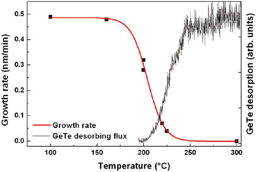
However, before discussing the effect of the substrate orientation, we first consider fundamental aspects that similarly influence the growth for both substrate orientations: desorption and growth temperature. Experimentally it is found that there is a temperature window that allows for epitaxial growth [Citation18,21,45]. Below a substrate temperature of 180 °C, GST films grown by MBE were found to be polycrystalline, whereas amorphous GST was deposited at even lower temperatures [Citation18]. Figure shows the GST deposition rate and the desorption of GeTe as measured by QMS as a function of GaSb(0 0 1) substrate temperature [Citation45]. It can be seen that the desorption of GeTe starts at a temperature above 200 °C and is accompanied by a decrease in the deposition rate. At higher temperatures, the ability to grow epitaxial layers is thus limited by the desorption of the GeTe molecules. For typical growth rates employed in MBE 0.4–0.9 nm/min, this limits the growth window to approximately 180–250 °C. Growth rates up to 250 nm/min are possible using PLD [Citation22] and for growth rates of 5 nm/min a notable desorption only sets in above 300 °C [Citation22] compared to an onset at 200 °C for MBE [Citation45]. The higher onset of desorption cannot only be explained by the increased growth rate of PLD. The difference in background pressure should also be taken into account, being <10−9 mbar [Citation18] and 4 × 10⁻⁵ mbar [Citation22] during MBE and PLD growth, respectively. Furthermore, a difference in nucleation between the different deposition conditions might contribute to the effect. Interestingly, an increase in the growth temperature has opposite effects on the stoichiometry of the deposited films. For films deposited by MBE, an increase in the growth temperature results in a higher Ge content of the film [Citation46], whereas an antimony enrichment is observed at higher growth temperatures for films grown by PLD [Citation22]. It is presently unclear what causes this difference.
Figure 4. The deposition rate and the GeTe desorption as a function of GaSb(0 0 1) substrate temperature.
The lowest reported temperature limit for growing epitiaxial GST is realized using PLD at a remarkable value of 85 °C [Citation21]. This is in fact lower than the crystallization temperature of GST [Citation2] and shows a benefit of the non-thermal nature of growth by PLD. Finally, it should be mentioned that monitoring the growth temperatures in the range of 200–300 °C is rather difficult because normal pyrometers cannot be used in this temperature range and measurements by thermocouples are often imprecise because there is no direct contact with the wafer. QMS, monitoring the amount of desorbing material from a surface, can be used as a probe of the surface temperature during the deposition. In such an experiment, it was concluded that the effective temperature of the substrate surface increases by 20–30 °C during the deposition by MBE [Citation46]. This was attributed to the increased heat absorption by GST due to the lower band gap of GST with respect to the substrate. By adjusting the thermocouple temperature during the deposition, the desorption and hence the surface temperature could be held constant.
4.1. (0 0 1)-oriented substrates
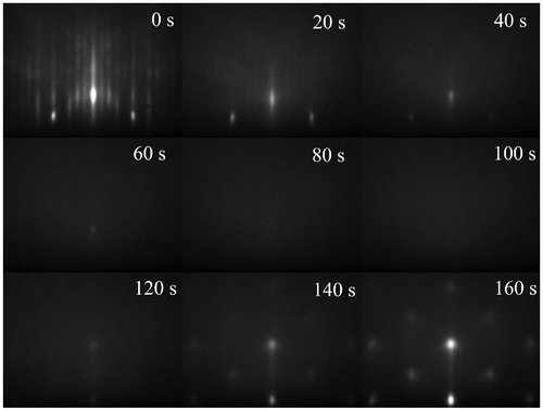
As mentioned above, the first epitaxial GST films were grown on GaSb(0 0 1) [Citation18]. Therefore, we will use this substrate as a starting point for our discussion on the growth on (0 0 1)-oriented substrates. GaSb has a lattice constant of 6.096 Å and thus has a lattice mismatch of 1.1% with respect to metastable cubic GST, which has a lattice constant of 6.029 Å [Citation30]. Besides this lattice mismatch there is also a symmetry mismatch. GaSb has the zincblend structure and GST the rocksalt structure. RHEED investigations revealed an interesting phenomenon that occurs during the initial growth GST on GaSb(0 0 1). Figure shows RHEED patterns taken during the initial stage of the growth on GaSb(0 0 1). Prior to the beginning of the growth one can see a nice diffraction pattern of the reconstructed surface of GaSb. As soon as the deposition starts, the intensity of the diffraction pattern is reduced and after 100 s no RHEED pattern is observed, indicative that the deposited film is amorphous. After a certain amount of time (120 s in this case) diffraction peaks are again observed, indicating that the film has become crystalline. It is here important to point out that the whole film has crystallized, as determined by electron microscopy after the deposition. Shayduk and Braun observed that the occurrence of the amorphous stage is suppressed at higher growth temperatures [Citation47]. Moreover, it was found to be absent when films were grown on InAs(0 0 1) [Citation48], indicating that it depends on the substrate–film interface. Recent studies also observed this transition for the growth of GeTe on Si(1 1 1)-7 × 7,[Citation49] but not for the growth of GeTe on Si(1 1 1)-√3 × √3-Sb [Citation50], which is consistent with this picture. Wang et al. related this transition to the different types of bonding present in conventional semiconductors, such as GaSb and Si, and PCM, such as GST [Citation51].
Figure 5. RHEED diffraction patterns taken during the deposition of GST on GaSb(0 0 1).
Another typical feature for GST films grown on (0 0 1)-oriented substrates can be seen in Figure . The RHEED pattern of the crystalline GST shows clear transmission spots, indicative of a rough surface. Such transmission spots have also been observed for GST films grown on InAs(0 0 1) [Citation45], which has a lower lattice mismatch (0.5%) with GST. Scanning electron microscopy (SEM), transmission electron microscopy (TEM), and RHEED investigations of films grown on GaSb(0 0 1) revealed that the surface of (0 0 1)-oriented films is prone to faceting [Citation18,45,47]. These facets have a (1 1 1) orientation, suggesting that these surfaces are those with the lowest energy. AFM investigations of (0 0 1)-oriented films grown by PLD also revealed a large surface roughness caused by crystallites forming a fishbone pattern [Citation22]. Moreover, TEM investigations of (0 0 1)-oriented GST also revealed a large interface roughness between GaSb and GST [Citation45]. These observations show that the (0 0 1)-surface/interface of GST is unstable.
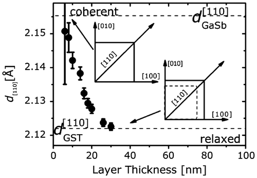
Grazing incidence X-ray diffraction (XRD) investigations of GST films grown on GaSb(0 0 1) revealed that the GST films consisted of domains with the [0 0 1] and the [1 1 1] directions parallel to the [0 0 1] direction of the GaSb substrate [Citation18]. The coexistence of [0 0 1]- and [1 1 1]-oriented grains was also found in GST films grown by PLD on (0 0 1)-oriented KCl [Citation22]. Moreover, it was found that GST films grown on (0 0 1)-oriented Si have almost a full out-of-plane [1 1 1] orientation [Citation48]. Since the (0 0 1) orientation is favored by the substrate, it is concluded that the GST prefers to have its (1 1 1) plane parallel to the surface. This is consistent with a lower surface energy of this surface, as discussed above. Interestingly, Thelander et al. found that the GST orientation depends on the deposition temperature [Citation22]. For growth at 230 °C they obtained a largely (1 1 1)-oriented film, whereas the main orientation of films grown at 290 °C was found to be (0 0 1) [Citation22]. Moreover, they found that part of 68-nm-thick GST film grown at 290 °C had an out-of-plane [2 2 1] direction [Citation22]. Note that this later growth regime has not been studied by MBE because the combination of a relatively low growth rate and desorption prevents the growth of GST in this regime by MBE. In order to overcome this limitation and confirm this observation, the flux rate for MBE grown films should be increased. Finally, grazing incidence XRD has been used to study the in-plane lattice constant of GST grown on GaSb(0 0 1) [Citation52]. Figure shows the in-plane lattice constant of GST as a function of layer thickness. It shows that the crystalline GST formed after disappearance of the amorphous phase is almost coherently strained to the GaSb substrate. The strain is relaxed during the growth and is fully relaxed for thicknesses above 30 nm. Such a relaxation of the strain is typical for lattice mismatched materials.
Figure 6. In-plane lattice constant of GST grown on GaSb(0 0 1) as a function of layer thickness.
4.2. (1 1 1)-oriented substrates
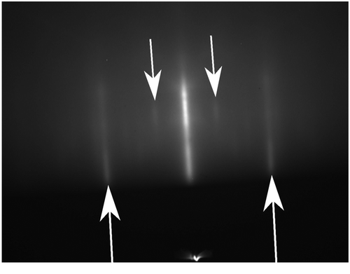
The growth of GST on (1 1 1)-oriented substrates differs significantly from the growth on (0 0 1)-oriented substrate and can be considered as superior [Citation44,45]. An important difference between the growth on these two orientations is that the amorphous to crystalline transition, discussed above, is not observed for growth on (1 1 1)-oriented substrates. Instead, the GST is crystalline during the entire growth. This can for example be seen in the RHEED image in Figure . This image is taken 10 s after the start of the growth. The streaks corresponding to the GST crystal structure, indicated by the upward pointing arrows, are clearly observed. Besides, the GST diffraction peaks due to the Si(1 1 1)-√3 × √3 surface reconstruction, downward pointing arrows, are still observed. This indicates that the substrate surface is not fully covered. The fact that the GST is crystalline at the same time clearly shows the absence of an amorphous phase. Furthermore, RHEED pattern taking during the deposition shows that the GST lattice constant is immediately relaxed. This is similar to the growth of Sb2Te3 and other layered materials and is attributed to the small interaction between substrate and film occurring during van der Waals epitaxy [Citation53]. Interestingly, the presence of a small interaction with the substrate and films results in a surface reconstruction-induced coincidence lattice matching when GST is grown on Si(1 1 1)-7 × 7 [Citation54]. It is likely that the smaller interaction between (1 1 1)-oriented substrates and films also prevents the occurrence of an amorphous stage during the deposition because it reduces the electronic coupling between film and layer.
Figure 7. RHEED pattern taken 10 s after the start of the GST growth on Si(1 1 1)-√3 × √3.
XRD investigations show that GST films grown on (1 1 1)-oriented substrates have a (1 1 1) out-of-plane orientation [Citation44].This is also the case for films grown on insulating substrates, such as (1 1 1)-oriented BaF2 [Citation21]. The GST films normally have a well-defined in-plane alignment with the substrate, but presence of twins is common. The amount of twinning can be controlled to some extent by the substrate temperature during growth [Citation21] or using a (1 1 1)-oriented substrate with a deliberate miscut [Citation55]. Besides the (1 1 1) orientation of the GST films, XRD measurements also revealed the presence of additional peaks (VLp) in the θ-2θ diffraction patterns, shown in Figure (a). It was concluded that they belong to the vacancy ordered phase of GST for MBE-grown samples [Citation33] and to the trigonal phase for PLD-grown samples [Citation21]. Comparison with the expected peak positions of vacancy ordered GST, shown in the calculation displayed below the diffraction profile, revealed the presence of different stacking sequences in the film, such as GST225 and GST326. Hilmi et al. studied the mosaic spread of GST films grown on Si(1 1 1) using XRD rocking curve scans, i.e. Figure (b) and (c) [Citation23]. They found that the out-of-plane Bragg peak consists of two parts: a narrow one with a full width half maximum of 0.06° and a broader one that depends on the growth temperature. As shown in Figure (c), the narrow one is approximately constant, whereas the broad one ranges from 2.5° to 0.18°.
Figure 8. (a) XRD profile of an epitaxial GST film grown on Si(1 1 1)-√3 × √3 and the expected peak position for different GST phases. The observation of a broad vacancy layer peak (VLp) indicates that there is a distribution in the separation between the vacancy layers. Reproduced from Scientific Reports, 6, V. Bragaglia, F. Arciprete, W. Zhang, A.M. Mio, E. Zallo, K. Perumal, A. Giussani, S. Cecchi, J.E. Boschker, H. Riechert, S. Privitera, E. Rimini, R. Mazzarello and R. Calarco, Metal - Insulator Transition Driven by Vacancy Ordering in GeSbTe Phase Change Materials, 23843, (2016)[Citation33] - Published by Nature publishing Group. (b) Mosaic spread of a GST film grown on Si(1 1 1) as measured by XRD rocking curve measurements. (c) The reduction of the FWHM due to an increase in substrate temperature.
![Figure 8. (a) XRD profile of an epitaxial GST film grown on Si(1 1 1)-√3 × √3 and the expected peak position for different GST phases. The observation of a broad vacancy layer peak (VLp) indicates that there is a distribution in the separation between the vacancy layers. Reproduced from Scientific Reports, 6, V. Bragaglia, F. Arciprete, W. Zhang, A.M. Mio, E. Zallo, K. Perumal, A. Giussani, S. Cecchi, J.E. Boschker, H. Riechert, S. Privitera, E. Rimini, R. Mazzarello and R. Calarco, Metal - Insulator Transition Driven by Vacancy Ordering in GeSbTe Phase Change Materials, 23843, (2016)[Citation33] - Published by Nature publishing Group. (b) Mosaic spread of a GST film grown on Si(1 1 1) as measured by XRD rocking curve measurements. (c) The reduction of the FWHM due to an increase in substrate temperature.](/cms/asset/bedc9363-eec1-4d69-a04f-c441f833976e/tapx_a_1346483_f0008_oc.gif)
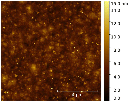
Another difference with respect to the growth on (0 0 1)-oriented substrates is the surface roughness of the layers. For films grown on (1 1 1)-oriented substrates, RHEED investigations typically show a streaky pattern, indicative of a smooth two-dimensional surface. It has been found that the surface roughness of films deposited on (1 1 1)-oriented substrate is lower compared to films grown on (0 0 1)-oriented substrate by MBE [Citation44,45] as well as for films grown by PLD [Citation22]. AFM investigations of (1 1 1)-oriented films, see Figure , show that the surface morphology is determined by the presence of triangular-shaped islands. One can observe two different orientations of the triangles, which is consistent with the presence of crystallographic twins in the GST layer. Such triangular-shaped islands are also typical for the growth of other layered materials, such as Sb2Te3 [Citation56]. They can be formed by spiral growth and thus have a dislocation in the center. However, in the case of layered materials, it is not necessarily an indication of the presence of dislocations propagating from the substrate because the spirals can also form at the substrate step edge [Citation57]. Finally, it should be noted that the use of excess Te during the deposition by MBE can result in the formation of Te precipitates on the GST surface.
Figure 9. AFM image of the surface of an epitaxial GST film grown on Si(1 1 1)-√3 × √3.
4.3. GeTe/Sb2Te3 superlattices
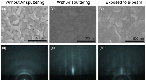
The integration of GeTe/Sb2Te3 superlattices (SLs) in phase change memory cells and the enhanced performance of such memory cells compared to cell based on conventional GST [Citation27] have resulted in an interest to understand the growth and properties of such SLs on crystalline as well as amorphous substrates. Growth of GeTe/Sb2Te3 SLs on amorphous substrates is typically commenced by the deposition of a Sb2Te3 layer [Citation27]. The layered structure of Sb2Te3 results in a preferential texture with a (0 0 0 1) out-of-plane orientation. This layer serves as a template for the subsequent growth of the SL. Experiments have shown that the quality of the texture depends sensitively on the substrate preparation, at least for the growth on oxides [Citation58]. Exposure to Ar+ ions or an electron beam prior to the deposition improved the out-of-plane texture significantly [Citation58,59]. In Figure , the surface morphology and crystal orientation of SL grown on SiO2 surfaces with different kind of surface preparations are shown. Figure (a) and (b) shows that the surface is rough on the untreated surface and the film has a random out-of-plane orientation, as evidenced by the polycrystalline rings observed in the RHEED pattern. For surfaces exposed to Ar+(Figure (c) and (d)) or high energy electrons (Figure (e) and (f)), a good texture and a low surface roughness were obtained. X-ray photoelectron spectroscopy studies showed that this surface preparation resulted in the formation of a silicon suboxide [Citation58]. The use of such a surface preparation was not necessary for carbon substrates [Citation58], indicating that the crystal growth strongly depends on the surface chemistry.
Figure 10. Scanning electron microscopy image (a,c & e) and RHEED patterns (B,d & f) of SL grown on SiO2 surfaces with different surface preparations.
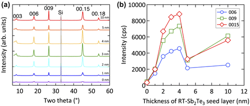
Another method to improve the texture on amorphous substrates is the use of a buffer layer [Citation58,60]. In this case, the first Sb2Te3 layer is grown below the crystallization temperature of Sb2Te3 and is thus initially amorphous. Upon heating the substrate, the layer crystallizes, obtains a good texture, and can be used as a template for the growth of the SL. Saito et al. studied the effect of the buffer layer thickness on the XRD profiles of Sb2Te3 layer grown on the buffer layer. The data in Figure (a) and (b) show that the intensity of the Sb2Te3 diffraction peaks has a maximum for a buffer layer of 3–4 nm. Hence, they concluded that this is the optimum buffer layer thickness.
Figure 11. (a) XRD diffraction profiles and (b) peak intensities of Sb2Te3 thin films grown with buffer layers with different thickness.
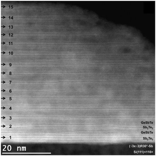
Using this approach, Saito et al. subsequently grew GeTe/Sb2Te3 SL. Figure (a) shows a cross-sectional TEM image of such a SL. It can clearly be seen that the SL has a high quality, as deduced from the low surface roughness, large domain size (approximately 200 nm), and the clear diffraction pattern Figure (b). Even though highly textured films can be obtained using this approach, the in-plane orientation remains random. Epitaxial growth overcomes this problem and the growth of epitaxial GeTe/Sb2Te3 SLs by MBE has thus greatly facilitated their characterization [Citation24,61–63]. Figure shows a STEM image of such a heterostructure. Several important observations were made. First, it was shown that GeTe/Sb2Te3 SL are unstable and transform into trigonal GST upon annealing. Secondly, it was shown that the GeTe layer reacts with 1 nm of the Sb2Te3 and thus forms a GST alloy. This was subsequently also concluded by analyzing GeTe/Sb2Te3 samples grown by sputtering [Citation24]. In a later work, a model describing the intermixing occurring during MBE growth was also presented [Citation63]. These results showed that the switching mechanism in GeTe/Sb2Te3 should be reconsidered.
Figure 12. (a) Transmission electron microscopy image and (b) electron diffraction pattern of a SL grown using a buffer layer.
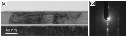
Figure 13. Transmission electron microscopy image of an epitaxial SL.
5. Outlook
During the last decade, impressive progress has been made in the growth of crystalline PCM by means of physical deposition methods. Nevertheless, some challenges remain. For example, the growth of a pure cubic or a pure trigonal GST alloy has not been achieved using these methods. The ability to do so would expand the possibilities of investigating the fundamental properties of GST. The reduction of twinning is also expected to significantly improve the quality of epitaxial GST. At present, it represents an open challenge as it is unclear how this could be achieved. Another interesting direction that has not been attempted yet is the epitaxial growth of PCM, such as Ag5In6Sb59Te30 (AIST). We hope that this review will serve as a reference for future investigation of the growth of PCM and inspire researchers in order to improve the growth of crystalline PCM.
Disclosure statement
No potential conflict of interest was reported by the authors.
Funding
This work was supported by the Leibniz Gemeinschaft within the Leibniz Competition on a project entitled: ‘Epitaxial phase change superlattices designed for investigation of non-thermal switching’.
Acknowledgements
V. Bragaglia is kindly acknowledged for providing Figure . We would like to thank all the people that worked on PCM at PDI for their contribution to this field and M. Hanke for critical reading of the manuscript.
References
- M. Wuttig and N. Yamada, Nat. Mater. 6 (2007) p.824.10.1038/nmat2009
- N. Yamada, E. Ohno, K. Nishiuchi, N. Akahira, M. Takao, J. Appl. Phys. 69 (1991) p.2849.10.1063/1.348620
- G.W. Burr, M.J. BrightSky, A. Sebastian, H.-Y. Cheng, J.-Y. Wu, S. Kim, N. E. Sosa, N. Papandreou, H.-L. Lung, H. Pozidis, E. Eleftheriou, C. H. Lam, IEEE J. Emerg. Sel. Top. Circuits Syst. 6 (2016) p.146.10.1109/JETCAS.2016.2547718
- S. Raoux, W. Wełnic, D. Ielmini, Chem. Rev. 110 (2010) p.240.10.1021/cr900040x
- P. Hosseini, C.D. Wright, H. Bhaskaran, Nature 511 (2014) p.206.10.1038/nature13487
- C. Ríos, M. Stegmaier, P. Hosseini, D. Wang, T. Scherer, C.D. Wright, H. Bhaskaran, W.H.P. Pernice, Nat Phot. 9 (2015) p.725.10.1038/nphoton.2015.182
- T. Tuma, A. Pantazi, M. Le Gallo, A. Sebastian, E. Eleftheriou, Nat. Nanotechnol. 11 (2016) p.693.10.1038/nnano.2016.70
- G.W. Burr, R.M. Shelby, A. Sebastian, S. Kim, S. Kim, S. Sidler, K. Virwani, M. Ishii, P. Narayanan, A. Fumarola, L. L. Sanches, I. Boybat, M. Le Gallo, K. Moon, J. Woo, H. Hwang, Y. Leblebici, Adv. Phys. X 2 (2017) p.89.
- M. Wuttig and S. Raoux, Zeitschrift für Anorg. und Allg. Chemie 638 (2012) p.2455.
- K. Shportko, S. Kremers, M. Woda, D. Lencer, J. Robertson, M. Wuttig, Nat. Mater. 7 (2008) p.653.10.1038/nmat2226
- B. Huang and J. Robertson, Phys. Rev. B 81 (2010) p.81204.10.1103/PhysRevB.81.081204
- J. Orava, A. Greer, B. Gholipour, D. Hewak, C. Smith, Nat. Mater. 11 (2012) p.279.10.1038/nmat3275
- M. Salinga, E. Carria, A. Kaldenbach, M. Bornhöfft, J. Benke, J. Mayer, M. Wuttig, Nat. Commun. 4 (2013) p.2371.
- P. Fons, H. Osawa, A. V. Kolobov, T. Fukaya, M. Suzuki, T. Uruga, N. Kawamura, H. Tanida, J. Tominaga, Phys. Rev. B 82 (2010) p.41203.10.1103/PhysRevB.82.041203
- A.V. Kolobov, P. Fons, J. Tominaga, Phys. Status Solidi B 251 (2014) p.1297.10.1002/pssb.201350146
- A.V. Kolobov, P. Fons, J. Tominaga, Sci. Rep. 5 (2015) p.13698.10.1038/srep13698
- A.V. Kolobov, P. Fons, A. I. Frenkel, A. L. Ankudinov, J. Tominaga, T. Uruga, Nat. Mater. 3 (2004) p.703.10.1038/nmat1215
- W. Braun, R. Shayduk, T. Flissikowski, M. Ramsteiner, H. T. Grahn, H. Riechert, P. Fons, A. V. Kolobov, Appl. Phys. Lett. 94 (2009) p.41902.10.1063/1.3072615
- C. Pauly, M. Liebmann, A. Giussani, J. Kellner, S. Just, J. Sánchez-Barriga, E. Rienks, O. Rader, R. Calarco, G. Bihlmayer, M. Morgenstern, Appl. Phys. Lett. 103 (2013) p.243109.10.1063/1.4847715
- U. Ross, A. Lotnyk, E. Thelander, B. Rauschenbach, J. Alloys Compd. 676 (2016) p.582.10.1016/j.jallcom.2016.03.159
- E. Thelander, J. W. Gerlach, U. Ross, A. Lotnyk, B. Rauschenbach, Appl. Phys. Lett. 105 (2014) p.221908.10.1063/1.4903489
- E. Thelander, J. W. Gerlach, U. Ross, F. Frost, B. Rauschenbach, J. Appl. Phys. 115 (2014) p.213504.10.1063/1.4879419
- I. Hilmi, E. Thelander, P. Schumacher, J. W. Gerlach, B. Rauschenbach, Thin Solid Films 619 (2016) p.81.10.1016/j.tsf.2016.10.028
- J. Momand, F. R. L. Lange, R. Wang, J. E. Boschker, M. A. Verheijen, R. Calarco, M. Wuttig, B. J. Kooi, J. Mater. Res. 31 (2016) p.3115.10.1557/jmr.2016.334
- H. Hardtdegen, S. Rieß, M. Schuck, K. Keller, P. Jost, H. Du, M. Bornhöfft, A. Schwedt, G. Mussler, M. v.d. Ahe, J. Mayer, G. Roth, D. Grützmacher, M. Mikulics, J. Alloys Compd. 679 (2016) p.285.10.1016/j.jallcom.2016.04.013
- M. Schuck, S. Rieß, M. Schreiber, G. Mussler, D. Grützmacher, H. Hardtdegen, J. Cryst. Growth 420 (2015) p.37.10.1016/j.jcrysgro.2015.03.034
- R.E. Simpson, P. Fons, A. V. Kolobov, T. Fukaya, M. Krbal, T. Yagi, J. Tominaga, Nat. Nanotechnol. 6 (2011) p.501.10.1038/nnano.2011.96
- H. Hardtdegen, M. Mikulics, S. Rieß, M. Schuck, T. Saltzmann, U. Simon, M. Longo, Prog. Cryst. Growth Charact. Mater. 61 (2015) p.27.10.1016/j.pcrysgrow.2015.10.001
- W.Z. Ostwald, Zeitschrift für Phys: Chemie 22 (1897) p.289.
- T. Matsunaga, N. Yamada, Y. Kubota, Acta Crystallogr. B. 60 (2004) p.685.10.1107/S0108768104022906
- W. Zhang, A. Thiess, P. Zalden, R. Zeller, P. H. Dederichs, J.-Y. Raty, M. Wuttig, S. Blügel, R. Mazzarello, Nat. Mater. 11 (2012) p.952.10.1038/nmat3456
- A.M. Mio, S. M. S. Privitera, V. Bragaglia, F. Arciprete, C. Bongiorno, R. Calarco, E. Rimini, Nanotechnology 28 (2017) p.65706.10.1088/1361-6528/28/6/065706
- V. Bragaglia, F. Arciprete, W. Zhang, A. M. Mio, E. Zallo, K. Perumal, A. Giussani, S. Cecchi, J. E. Boschker, H. Riechert, S. Privitera, E. Rimini, R. Mazzarello, R. Calarco, Sci. Rep. 6 (2016) p.23843.10.1038/srep23843
- B. Zhang, W. Zhang, Z. Shen, Y. Chen, J. Li, S. Zhang, Z. Zhang, M. Wuttig, R. Mazzarello, E. Ma, X. Han, Appl. Phys. Lett. 108 (2016) p.191902.10.1063/1.4949011
- I.I. Petrov, R. M. Imamov, Z. G. Pinsker, Sov. Phys. - Crystallogr. 13 (1968) p.339.
- B.J. Kooi and J.T.M. De Hosson, J. Appl. Phys. 92 (2002) p.3584.10.1063/1.1502915
- A. Lotnyk, U. Ross, S. Bernütz, E. Thelander, B. Rauschenbach, Sci. Rep. 6 (2016) p.26724.10.1038/srep26724
- J. Houška, E. M. Peña-Méndez, J. Kolář, J. Přikryl, M. Pavlišta, M. Frumar, T. Wágner, J. Havel, Rapid Commun. Mass Spectrom. 28 (2014) p.699.
- G.J.H.M. Rijnders, G. Koster, D. H. A. Blank, H. Rogalla, Appl. Phys. Lett. 70 (1997) p.1888.10.1063/1.118687
- J.P. Podkaminer, J. J. Patzner, B. A. Davidson, C. B. Eom, APL Mater. 4 (2016) p.86111.10.1063/1.4961503
- I. Hilmi, Lotnyk, J. W. Gerlach, P. Schumacher, B. Rauschenbach, APL Mater. 5 (2017) p.50701.10.1063/1.4983403
- J.E. Boschker, E. Folven, Å. F. Monsen, E. Wahlström, J. K. Grepstad, T. Tybell, Cryst. Growth Des. 12 (2012) p.562.10.1021/cg201461a
- J.E. Boschker, M. Boniardi, A. Redaelli, H. Riechert, R. Calarco, Appl. Phys. Lett. 106 (2015) p.23117.10.1063/1.4906060
- P. Rodenbach, R. Calarco, K. Perumal, F. Katmis, M. Hanke, A. Proessdorf, W. Braun, A. Giussani, A. Trampert, H. Riechert, P. Fons, A. V. Kolobov, Phys. Status Solidi Rapid Res. Lett. 6 (2012) p.415.10.1002/pssr.v6.11
- F. Katmis, R. Calarco, K. Perumal, P. Rodenbach, A. Giussani, M. Hanke, A. Proessdorf, A. Trampert, F. Grosse, R. Shayduk, R. Campion, W. Braun, H. Riechert, Cryst. Growth Des. 11 (2011) p.4606.10.1021/cg200857x
- K. Perumal, W. Braun, H. Riechert, R. Calarco, J. Cryst. Growth 396 (2014) p.50.10.1016/j.jcrysgro.2014.03.039
- R. Shayduk and W. Braun, J. Cryst. Growth 311 (2009) p.2215.10.1016/j.jcrysgro.2008.11.028
- K. Perumal, Epitaxial Growth of Ge-Sb-Te Based Phase Change Materials, Humboldt-Universität zu Berlin, Berlin, 2013.
- A. Giussani, K. Perumal, M. Hanke, P. Rodenbach, H. Riechert, R. Calarco, Phys. Status Solidi 249 (2012) p.1939.10.1002/pssb.201200367
- R. Wang, J. E. Boschker, E. Bruyer, D. Di Sante, S. Picozzi, K. Perumal, A. Giussani, H. Riechert, R. Calarco, J. Phys. Chem. C 118 (2014) p.29724.10.1021/jp507183f
- R. Wang, W. Zhang, J. Momand, I. Ronneberger, J. E. Boschker, R. Mazzarello, B. J. Kooi, H. Riechert, M. Wuttig, R. Calarco, NPG Asia Mater. accepted (2017).
- F. Katmis, M. Schmidbauer, S. M. Bokoch, P. Rodenbach, H. Riechert, R. Calarco, Phys. Status Solidi 251 (2014) p.769.10.1002/pssb.201350138
- A. Koma, Thin Solid Films 216 (1992) p.72.10.1016/0040-6090(92)90872-9
- J.E. Boschker, J. Momand, V. Bragaglia, R. Wang, K. Perumal, A. Giussani, B. J. Kooi, H. Riechert, R. Calarco, Nano Lett. 14 (2014) p.3534.10.1021/nl5011492
- E. Zallo, S. Cecchi, J. E. Boschker, A. M. Mio, F. Arciprete, S. Privitera, R. Calarco, Sci. Rep. 7 (2017) p.1466.10.1038/s41598-017-01502-z
- J.E. Boschker, L. A. Galves, T. Flissikowski, J. M. J. Lopes, H. Riechert, R. Calarco, Sci. Rep. 5 (2015) p.18079.
- Y. Liu, M. Weinert, L. Li, Phys. Rev. Lett. 108 (2012) p.115501.10.1103/PhysRevLett.108.115501
- J.E. Boschker, E. Tisbi, E. Placidi, J. Momand, A. Redaelli, B. J. Kooi, F. Arciprete, R. Calarco, AIP Adv. 7 (2017) p.15106.10.1063/1.4974464
- Y. Saito, P. Fons, A. V. Kolobov, J. Tominaga, Phys. Status Solidi 252 (2015) p.2151.10.1002/pssb.v252.10
- Y. Saito, P. Fons, L. Bolotov, N. Miyata, A. V Kolobov, J. Tominaga, AIP Adv. 6 (2016) p.45220.10.1063/1.4948536
- J. Momand, R. Wang, J. E. Boschker, M. A. Verheijen, R. Calarco, B. J. Kooi, Nanoscale 7 (2015) p.19136.10.1039/C5NR04530D
- B. Casarin, A. Caretta, J. Momand, B. J. Kooi, M. A. Verheijen, V. Bragaglia, R. Calarco, M. Chukalina, X. Yu, J. Robertson, F. Lange, M. Wuttig, A. Redaelli, E. Varesi, F. Parmigiani, M. Malvestuto, Sci. Rep. 6 (2016) p.22353.10.1038/srep22353
- R. Wang, V. Bragaglia, J. E. Boschker, R. Calarco, Cryst. Growth Des. 16 (2016) p.3596.10.1021/acs.cgd.5b01714
- R. Shayduk, F. Katmis, W. Braun, H. Riechert, J. Vac. Sci. Technol. B 28 (2010) p.1.
- I. Hilmi, Lotnyk, J. W. Gerlach, P. Schumacher, B. Rauschenbach, Mater. Des. 115 (2017) p.138.10.1016/j.matdes.2016.11.003
- K. Momma and F. Izumi, J. Appl. Crystallogr. 44 (2011) p.1272.10.1107/S0021889811038970
- A. Lotnyk, S. Bernütz, X. Sun, U. Ross, M. Ehrhardt, B. Rauschenbach, Acta Mater. 105 (2016) p.1.10.1016/j.actamat.2015.12.010