
 ?Mathematical formulae have been encoded as MathML and are displayed in this HTML version using MathJax in order to improve their display. Uncheck the box to turn MathJax off. This feature requires Javascript. Click on a formula to zoom.
ABSTRACT
Photovoltaic (PV) conversion of solar energy starts to give an appreciable contribution to power generation in many countries, with more than 90% of the global PV market relying on solar cells based on crystalline silicon (c-Si). The current efficiency record of c-Si solar cells is 26.7%, against an intrinsic limit of ~29%. Current research and production trends aim at increasing the efficiency, and reducing the cost, of industrial modules. In this paper, we review the main concepts and theoretical approaches that allow calculating the efficiency limits of c-Si solar cells as a function of silicon thickness. For a given material quality, the optimal thickness is determined by a trade-off between the competing needs of high optical absorption (requiring a thicker absorbing layer) and of efficient carrier collection (best achieved by a thin silicon layer). The efficiency limits can be calculated by solving the transport equations in the assumption of optimal (Lambertian) light trapping, which can be achieved by inserting proper photonic structures in the solar cell architecture. The effects of extrinsic (bulk and surface) recombinations on the conversion efficiency are discussed. We also show how the main conclusions and trends can be described using relatively simple analytic models. Prospects for overcoming the 29% limit by means of silicon/perovskite tandems are briefly discussed.
Graphical Abstract
1. Introduction
Solar energy has the largest potential among renewable energy sources, and it can be transformed into usable electricity by photovoltaic (PV) conversion in solar cells. PV solar power is starting to give an appreciable contribution to the energy mix in many countries; for example, solar power contributes about 4% of the averaged grid electricity in the European Union, and more than 7% in countries like Germany and Italy [Citation1,Citation2]. The installed (cumulated) PV power has increased at a high rate (~30–40% per year) in the last 15 years and is growing rapidly worldwide, thanks to increased efficiency and to reduced costs of commercial PV modules. Actually the production costs of solar cells and modules have decreased to such an extent that the solar cell impacts for a fraction of the total cost, while more than 50% is due to electrical and other components (balance of system) and to indirect costs like installation, maintenance, insurance, financing. Thus, in order to reduce the overall cost of PV energy (known as the levelized cost of electricity), it is of paramount importance to increase the conversion efficiency (which impacts the total cost/watt), while the production cost of the solar cell has a lesser impact.
The world PV market is largely dominated (above 90%) by wafer-based silicon solar cells, due to several factors: silicon has a bandgap within the optimal range for efficient PV conversion, it is the second most abundant material on the earth’s crust, it is nontoxic and its technology is well mastered by chemical and semiconductor industries. The energy conversion efficiency of silicon solar cells in the lab reached a record value of 25% in 1999 (the PERL cell based on p-type silicon [Citation3,Citation4]) which stood unsurpassed for 15 years. The record efficiency rose to 25.6% in 2014 [Citation5] and to 26.7% in 2017 [Citation6,Citation7] thanks to the heterojunction (HJ) intrinsic thin layer technology based on thin a-Si passivating layers and on interdigitated back contacts (IBCs) on n-type silicon wafers. The efficiency of wafer-based silicon modules has reached 24.4% and is constantly rising both in the lab and in the market. The strength of silicon technology can best be appreciated by looking at the International Technology Roadmap for Photovoltaic [Citation8].
On the theoretical side, the limiting efficiency of single-junction solar cells was first calculated in a seminal paper by Shockley and Queisser [Citation9] by a thermodynamic treatment that assumes detailed balance. The main assumptions are that all the light above the semiconductor bandgap is absorbed, and that the excited electron-hole pairs can only decay by radiative recombination. For an incident blackbody radiation at T = 6000 K, the Shockley–Queisser efficiency has a maximum around 30% with an optimal bandgap around 1.1 eV. When the incident radiation is taken to be the real AM1.5G solar spectrum, the thermodynamic efficiency limit is calculated to be around 33% [Citation10], the optimal bandgap range being between 1.1 and 1.4 eV. For the case of silicon, which has an indirect bandgap at 1.12 eV and long radiative recombination lifetimes, nonradiative Auger recombination of electron-hole pairs strongly limits the radiative efficiency and reduces the maximum conversion efficiency to about 29% [Citation10,Citation11]. The optimal crystalline silicon (c-Si) thickness is calculated to be ~100 µm. In real solar cells, extrinsic recombination mechanisms like defect-related (Shockley–Read–Hall, SRH) and surface recombination reduce the efficiency below the limiting values. Such effects were often investigated using a simplified model based on the ideal diode equation [Citation10,Citation12–Citation14]. Further effects like incomplete absorption of incident light and nonideal contacts play an important role in real solar cells. A nice review of older approaches to the efficiency limits is given by Swanson [Citation15].
In this paper, we review the limits to conversion efficiency in solar cells made of c-Si and analyze the role of extrinsic (nonradiative) recombination processes on the conversion efficiency. The emphasis is on the thickness dependence of the calculated figures of merit (conversion efficiency, short-circuit current, open-circuit voltage, fill factor (FF)) in order to understand how the optimum thickness changes for given material quality and target performance. Our results are based on theoretical models with different levels of complexity: in particular, we compare the results of analytic treatments with those of full device simulations that employ numerical solutions of the transport equations. For the case of ideal light trapping (see below), most results can be reproduced by an analytic model, validated against the full numerical simulations and implemented in a freely available Python code.
A properly designed solar cell has to be optically thick (i.e. to absorb all or most of the incident sunlight) and electronically thin (i.e. to collect the photoexcited electron-hole pairs with little or no losses). These two requirements lead to an optimal thickness that maximizes the efficiency. Thus, in order to understand the limiting efficiency we need to tackle both the optical and the electronic problem. In view of this, the rest of this paper is organized as follows. In Section 2, we briefly review the problem of light trapping in solar cells, with emphasis on the so-called Lambertian limit that is obtained in the presence of a scatterer that randomizes the optical path of light. In Section 3, we discuss full electro-optical calculations for selected photonic and solar cell structures. In Section 4, we assume the Lambertian limit for light trapping and evaluate the efficiency limits both for ideal c-Si solar cells and in the presence of bulk/surface recombination. Also, we briefly mention how the 29% efficiency limit can be potentially overcome by the use of tandem structures employing the recently discovered perovskite solar cells. Section 5 summarizes the main conclusions and the outlook.
2. Light trapping and Lambertian limit
Assuming 100% carrier collection, the short-circuit current density of a solar cell is given by the density of photogenerated carriers as:
where is the absorptance of the photoactive layer (i.e. the spectrally resolved absorption probability), and
is the photon flux corresponding to the AM1.5G solar spectrum. For a thickness
and an absorption coefficient
, neglecting reflection losses, the single-pass absorptance is simply given by
, as in the scheme of ). Usually, solar cells have a metal back reflector (BR) characterized by high reflectivity and low loss, which nearly doubles the optical path of light. To increase the optical path beyond the single- or double-pass absorption, we need to apply proper light-trapping schemes, based on surface texturization or on the insertion of scatterers (or a combination of both). This problem was first considered by Yablonovitch in two influential papers [Citation16,Citation17], where the top surface of the solar cell was assumed to act as a Lambertian scatterer that fully randomizes the optical path of light, as schematically shown in ). In the ray-optics case and in the limit of weak absorption, the effect of a Lambertian scatterer is to increase the light path by a factor
, where
is the refractive index of the sample. This enhancement factor can also be related to the increase of the optical density of states within the absorbing layer that results from total internal reflection [Citation16]. In the general case of Lambertian light trapping with arbitrary absorption, the increased absorptance and the electric field distribution within the sample can be calculated by the approach developed by Green [Citation18].
Figure 1. Schematic geometry of (a) a solar cell with a single layer leading to single-pass absorption or (b) a layer with a Lambertian scatterer in the front and a back reflector in the rear side, leading to Lambertian light trapping; (c) short-circuit current density for c-Si, a-Si:H, GaAs, and CIGS (taking
) as a function of thickness, under AM1.5 solar spectrum. Dashed lines refer to the single-pass case, while solid lines refer to the Lambertian limit with
, as defined in Ref. [Citation18]. Reflection losses are neglected throughout. Notice that the silicon curves differ from those published in Ref. [Citation23], due to the use of different data for c-Si [Citation19,Citation24] and for a-Si:H [Citation20].
![Figure 1. Schematic geometry of (a) a solar cell with a single layer leading to single-pass absorption or (b) a layer with a Lambertian scatterer in the front and a back reflector in the rear side, leading to Lambertian light trapping; (c) short-circuit current density Jsc for c-Si, a-Si:H, GaAs, and CIGS (taking x=0.08) as a function of thickness, under AM1.5 solar spectrum. Dashed lines refer to the single-pass case, while solid lines refer to the Lambertian limit with Rb=1, as defined in Ref. [Citation18]. Reflection losses are neglected throughout. Notice that the silicon curves differ from those published in Ref. [Citation23], due to the use of different data for c-Si [Citation19,Citation24] and for a-Si:H [Citation20].](/cms/asset/17323ce6-5ce7-4491-a2c0-0802e01ebd83/tapx_a_1548305_f0001_oc.jpg)
The results for the photocurrent as a function of material thickness are shown in ) for c-Si, using recent data for its optical functions [Citation19], and for other common PV materials with direct bandgap, namely hydrogenated amorphous silicon (a-Si:H) [Citation20], gallium arsenide (GaAs) [Citation21], and CuInGa
Se
(CIGS) [Citation22]. The case of cadmium telluride (CdTe) [Citation23] is similar to GaAs, as their bandgaps are nearly identical. Dashed lines refer to single-pass absorption, while solid lines refer to the case of Lambertian light trapping [Citation18]. It can first be seen that the photocurrent calculated with single-pass absorption is quite low for silicon, due to its indirect bandgap, unless the thickness exceeds several tens of microns. For direct bandgap materials, on the other hand, a few microns are already sufficient to yield full absorption and the maximum photocurrent. Light trapping is imperative in c-Si, as it allows to obtain a high photocurrent with a thickness around 100–200 µm [Citation24]. The current industrial standard for wafer-based silicon solar cells is 180 µm [Citation8]. The results of ) are valid in the ray-optics regime, such that the thickness is much larger than the wavelength of visible light. In this regime, surface texturization approaching the Lambertian limit of light trapping is commonly achieved with random pyramids, which are easily obtained via chemical etching of the silicon surface [Citation25,Citation26]. An even better solution is provided by inverse pyramids arranged in a regular lattice: this type of texturization is implemented in the PERL cell, but is not suitable for industrial production as it requires a lithographic step.
Notice that the limit of Lambertian light trapping amounts to consider zero reflection losses as well as maximum absorption in the solar cell material. In order to optimize both antireflection and light-trapping action, it may be useful to have only an antireflection coating (ARC) on the top surface, and to insert the scattering layer on the rear surface. In the Lambertian limit, the spectrally resolved photogeneration rate profile of the excited electron-hole pairs is given in closed form as [Citation27]:
where is the refractive index, and
is the reflectance of the rear mirror. In Equation (2),
denotes the effective absorption coefficient defined as
, where
is the absorption coefficient of the cell material, and
represents the optical path enhancement calculated in Ref. [Citation18]. In the following sections, we show that the carrier generation rate of Equation (2) can be usefully employed to reduce the full three-dimensional (3-D) electro-optical problem to a much simpler one-dimensional (1-D) problem depending only on the variable
, leading to analytic solutions of the transport equations.
In the last few years, much interest and intense research has been focused on the problem of light trapping in thin-film solar cells in the wave-optics limit, i.e. when the cell thickness is of the order of the wavelength of light. This is usually called the regime of photonic light trapping and it can be realized with structures that are either periodic (diffraction gratings or photonic crystals [Citation23,Citation28–Citation51]), modulated or aperiodic [Citation52–Citation55], disordered [Citation56–Citation69], quasi-random or with correlated disorder [Citation70–Citation72]. For reviews of the light-trapping problem and/or comparison of different structures, see Refs [Citation73–Citation78].
Considering the case of silicon material, an important clarification has to be made here. Solar cells based on noncrystalline (amorphous or micro-crystalline) silicon fall among the class of thin-film devices, i.e. solar cells with a thickness of the order of a micron (200–300 nm for a-Si, ~2 µm for microcrystalline silicon). Clever light-trapping schemes have been implemented for such silicon-based thin-film solar cells; however, their stabilized conversion efficiency remains low (less than about 11% for single-junction cells, less than ~14% for multijunctions) due to the poor quality of the noncrystalline material and of the interfaces. Solar cells based on amorphous/microcrystalline silicon are running out of the market as their low efficiencies make the cost per watt to be noncompetitive. Solar cells based on c-Si face the problem of low absorption in the infrared part of the spectrum due to the indirect bandgap. Ultrathin (micron-size) c-Si solar cells with Lambertian light trapping may have photocurrents slightly above 35 mA/cm2, see . The increase of the photocurrent over the single-pass value is substantial, but the absolute value of falls considerably short of the maximum practical value ~44 mA/cm2, thereby setting a limitation to actual conversion efficiencies.
The absolute limit of light trapping in the wave-optics regime is not known and it may exceed the Lambertian limit as defined above, especially in restricted spectral and/or angular ranges. It is not easy to compare the light-trapping efficiency in the presence of different photonic structures, as the reference thickness for the flat structure is not uniquely defined. The general issue of light-trapping limits in micron-sized absorbing layers has been addressed in a number of papers [Citation79–Citation84], for a recent reassessment on this debated problem see Ref. [Citation85]. We emphasize here that solar cells based on such ultra-narrow c-Si layers can hardly compete with conventional (wafer-based) silicon solar cells in terms of conversion efficiency. We show in this work that the range of thicknesses 20–100 µm is very interesting for solar cell performance, as it may lead to conversion efficiencies that exceed those of wafer-based silicon solar cells in realistic cases.
When considering light trapping in a wide range of thickness, say from ~1 to 200 µm, it is important to employ optical structures whose design is weakly dependent on thickness. Usual texturization based on random pyramids fulfills this criterion [Citation25]. We have studied another kind of texturization, namely a randomly rough interface with Gaussian disorder [Citation59,Citation60], whose design is also thickness independent to a large extent. The Gaussian disorder is defined by two parameters – the root mean square (RMS) height of the roughness and the in-plane correlation length – which can be optimized and yield a random structure approaching the Lambertian light trapping in a wide range of thicknesses. In the following section, we shall present examples of full electro-optical calculations of solar cells incorporating this kind of thickness-independent roughness.
3. Electro-optical modeling for thin-film silicon solar cells
Modeling the optical together with the electrical behavior of solar cells, especially in the presence of complex photonic structures for light trapping, is not a trivial task. Optical simulations covering both the wave-optics and the ray-optics regimes can be performed with well-known methods like rigorous coupled-wave analysis (RCWA) or finite-difference time-domain, while electrical simulations require the solution of transport equations with the finite-element method (FEM) or alike.
In this section, we briefly review an approach to electro-optical modeling of solar cells with photonic light trapping [Citation27,Citation86–Citation88], which relies on full optical simulations performed with the RCWA method. The electrical problem (i.e. the drift-diffusion equations for the p-n junction in the solar cell) is solved by the FEM method as implemented in the Silvaco-ATLAS software [Citation89], and we also compare with a simple 1-D model that allows for an analytic solution. We consider c-Si solar cells with Gaussian roughness for light trapping, focusing on the thickness dependence of the figures of merit and on the effect of extrinsic recombination. Our main goal is to understand realistic efficiency limits and prospects for thin-film c-Si solar cells produced with non-wafer-based techniques like layer transfer or liquid-phase recrystallization [Citation90–Citation95], which are needed for thicknesses below the wafer limit of ~80 µm.
In ), we show the photogeneration rate profile calculated by RCWA for a 10-µm thick c-Si layer with a randomly rough texture defined by Gaussian disorder. The photogeneration profile is integrated over the spectral interval from 1.1 to 4.2 eV and averaged over both polarizations. The photogeneration profile does not exhibit any mode pattern, as the roughness approaches a Lambertian scatterer. ) shows instead the solar cell structure that is considered in the electro-optical calculations. In the absorbing silicon layer, this includes a narrow and highly doped n-type emitter on top of a lightly doped p-type base. The spectrally resolved photogeneration profile calculated by RCWA is used as a source term in the drift-diffusion equations describing the transport of minority carriers in the silicon p-n junction. In the numerical approach, these equations are solved by the FEM. In principle, a 2-D surface roughness leads to a 3-D problem for the electronic transport. In practice, we consider a 1-D surface roughness and we rescale the photogeneration rate in order to account for isotropic scattering (see Ref. [Citation88] for details). This way, we need to solve only a 2-D electro-optical problem, which is a considerable simplification. In Ref. [Citation88], we also show that the photogeneration rate profile can be averaged over the parallel
direction and then fitted by the Lambertian profile of Equation (2), thereby allowing for an analytic approach. The solution of drift-diffusion equation in 1-D by the generalized Hovel model is described in the next section.
Figure 2. (a) Photogeneration profile of a 10-µm thick c-Si solar cell with Gaussian disorder, described by the RMS deviation of height nm and the lateral correlation length lc = 160 nm. The whole cell is shown in the inset, while the main plot shows the photogeneration profile close to the texture. All lengths are in µm. Reprinted from Ref. [Citation87], with the permission of AIP Publishing. (b) Structure considered in the FEM simulations. The p-n junction is made of an 80-nm thick n-type layer with donor concentration Nd = 1019 cm−3, and a p-type layer of thickness d−80 nm with acceptor concentration Na = 1016 cm−3. The ARC and silver layers serve as front and back contacts, respectively.
![Figure 2. (a) Photogeneration profile of a 10-µm thick c-Si solar cell with Gaussian disorder, described by the RMS deviation of height σ=300 nm and the lateral correlation length lc = 160 nm. The whole cell is shown in the inset, while the main plot shows the photogeneration profile close to the texture. All lengths are in µm. Reprinted from Ref. [Citation87], with the permission of AIP Publishing. (b) Structure considered in the FEM simulations. The p-n junction is made of an 80-nm thick n-type layer with donor concentration Nd = 1019 cm−3, and a p-type layer of thickness d−80 nm with acceptor concentration Na = 1016 cm−3. The ARC and silver layers serve as front and back contacts, respectively.](/cms/asset/436f28b7-c2c2-454b-8763-e1702188c977/tapx_a_1548305_f0002_oc.jpg)
In , we show the short-circuit current density , the open-circuit voltage
, the FF, and the efficiency
calculated with the FEM method, with materials parameters close to those of a c-Si solar cell fabricated by layer transfer [Citation90]. It should first be noticed that
increases with increasing thickness because of improved absorption, while
increases with decreasing thickness thanks to improved current collection. As a consequence, the conversion efficiency has a broad maximum
% for a thickness in the 10–50 µm range (the experimental value is 19% for a 43-µm thick cell [Citation90]). In Refs [Citation27,Citation88], we have shown that the approximate model based on fitting the photogeneration rate with a rescaled Lambertian profile agrees nicely with the full FEM simulations over a wide range of parameters, the main discrepancy being in the FF for very small thicknesses.
Figure 3. The main electrical parameters for c-Si solar cells without surface recombination: (a) open-circuit voltage and short-circuit current density
, (b) fill factor FF and conversion efficiency η. The diffusion lengths related to SRH recombination are LB = 232 µm for electrons in the p-type base [Citation90], and LE = 23.2 µm for holes in the n-type emitter [Citation25].
![Figure 3. The main electrical parameters for c-Si solar cells without surface recombination: (a) open-circuit voltage Voc and short-circuit current density Jsc, (b) fill factor FF and conversion efficiency η. The diffusion lengths related to SRH recombination are LB = 232 µm for electrons in the p-type base [Citation90], and LE = 23.2 µm for holes in the n-type emitter [Citation25].](/cms/asset/3e66e045-cf46-4575-86df-02b98a3fd7f4/tapx_a_1548305_f0003_oc.jpg)
Next, we study the effect of extrinsic recombination. In ), we plot the dependence of the conversion efficiency on the thickness and on the electron diffusion length in the base, which is mainly determined by SRH recombination. The efficiency increases with
and it may reach values above 25% when the diffusion length tends to macroscopic values. The high-efficiency limit will be properly discussed in the next section. The optimal values of the thickness for a given
are indicated by blue symbols and connecting lines. The optimal thickness increases with the diffusion length, i.e. with the material quality. In ), we display the conversion efficiency as a function of surface recombination velocity (SRV)
of minority electrons in the base. (It is shown in Ref. [Citation88] that the efficiency depends more critically on the back SRV than on the front SRV, as most of the photocurrent is generated in the base.) The conversion efficiency is generally reduced by surface recombination, especially for small thicknesses. The maximum efficiency around 20% is maintained as long as the SRV is below about
cm/s. Surface recombination below this level may be ensured by proper passivation or by a back surface field.
Figure 4. (a) Energy conversion efficiency for solar cells with perfect surface passivation (SB = SE = 0 cm/s) as a function of the electron diffusion length in the base (with LE = 23.2 µm) and of the cell thickness. The optimal configurations lie along the blue solid line with symbols. (b) Energy conversion efficiency as a function of the back surface recombination velocity
and of the cell thickness for LB = 232 µm, LE = 23.2 µm, and SE = 103 cm/s. All results are calculated by the FEM. Reprinted (with adaptation) from Ref. [Citation88], with permission from Elsevier.
![Figure 4. (a) Energy conversion efficiency for solar cells with perfect surface passivation (SB = SE = 0 cm/s) as a function of the electron diffusion length in the base LB (with LE = 23.2 µm) and of the cell thickness. The optimal configurations lie along the blue solid line with symbols. (b) Energy conversion efficiency as a function of the back surface recombination velocity SB and of the cell thickness for LB = 232 µm, LE = 23.2 µm, and SE = 103 cm/s. All results are calculated by the FEM. Reprinted (with adaptation) from Ref. [Citation88], with permission from Elsevier.](/cms/asset/428c05f5-4c6e-4c30-a8a6-656674a308c5/tapx_a_1548305_f0004_oc.jpg)
In this section, we have shown that modeling c-Si solar cells with photonic light trapping requires proper merging of optical and electrical simulations. Optical simulations with methods appropriate to the wave-optics limit provide the photogeneration rate profile of electron-hole pairs, which is used as an input to electrical simulations with the FEM. Complex photonic structures for light trapping impose the need of full 3-D electrical simulations. However, for nearly Lambertian light trapping, it is possible to implement a spatial averaging of the photogeneration profile, which reduces the electronic problem to a 1-D one and allows for an analytic solution of transport equations. Turning to the results, the conversion efficiency of c-Si solar cells has a maximum at a given value of the thickness, which is in the range 10–80 µm for typical parameters of non-wafer-based silicon. The maximum efficiency, as well as the optimal thickness, depends on nonradiative recombination processes via the diffusion length (for bulk or SRH) and via the SRV. Depending on material quality, the efficiency of such thin-film c-Si solar cells may compete with that of their bulk (wafer-based) counterparts. Future developments of thin-film c-Si solar cells will depend on progress in the material processes for the preparation of non-wafer-based silicon (layer transfer, liquid-phase recrystallization, and the like).
4. Efficiency limits with Lambertian light trapping
In this section, we tackle the more general problem of the efficiency limits in c-Si solar cells, assuming the structure to have no overall reflection and to contain ideal scattering interfaces that lead to Lambertian light trapping in the silicon layer. The photogeneration rate profile in the silicon layer is given by Equation (2), and we further assume perfect back reflection (). We thereby neglect all reflection or parasitic losses, and we also neglect free-carrier absorption which is a relatively minor effect [Citation10]. We do not consider radiative recombination and photon recycling: these two effects become important in the radiative limit, which is never realized in silicon as Auger recombination dominates under typical solar cell conditions. We consider Auger recombination according to a recent parameterization [Citation96] and we also include the effect of bandgap narrowing [Citation97], which is important when varying the doping concentrations.
We have studied the efficiency limits by comparing the results of three different models, here listed in order of increasing complexity:
4.1. Ideal diode equation
In this model, the J-V characteristic of the solar cell is given by
where is the short-circuit current density calculated assuming unity electron-hole pair collection efficiency (i.e. it corresponds to the photogenerated current density),
is again the cell thickness, and
is the total recombination rate per unit volume. This includes Auger, SRH, and also surface recombination [Citation98]. In this simplified model, a p-n junction does not explicitly appear, although it has still to be considered in order to quantify the effect of Auger recombination.
4.1.1. Generalized Hovel model
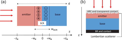
In this model, which was first formulated in Ref. [Citation99] for the case of thick solar cells with single-pass absorption, we solve the carrier transport equations with the source term given by the Lambertian photogeneration profile of Equation (2). Carrier dynamics is modeled under the assumption of the depletion region approximation [Citation25]. A space charge region (SCR) of width settles up across the junction plane, and is surrounded by two quasi-neutral (qn) regions, as schematically illustrated in ). The electrical transport in the SCR is dominated by the electric field which easily sweeps photogenerated carrier out of the region, allowing to neglect collection losses in the SCR. On the other hand, transport in the qn regions is dominated by diffusion of minority carriers and their collection is strongly affected by bulk or surface recombination. For the case of minority carriers in the base region, the diffusion equation under illumination may be written as:
Figure 5. (a) Scheme of the p-n junction for the generalized Hovel model. The impurity charges in the space charge region correspond to an n-emitter, p-base configuration, although the formulation of the model applies to both n-p and p-n configurations. The emitter is usually more narrow and highly doped than the base. (b) Scheme of the solar cell structure for the three models, including front and back contacts (serving also as ARC and back reflector, respectively) and the Lambertian scattering layer.
where denotes the excess carrier concentration,
is the diffusion constant, and
is the effective lifetime of minority carriers. This lifetime takes into account all possible recombination channels in the bulk, namely radiative (which is usually negligible in silicon), Auger, and SRH (defect-related). In the dark, when radiative and SRH contributions are evaluated from material parameters and doping levels, the diffusion length of minority carriers in the base is defined as
. This important parameter quantifies the material quality and is subject to requirements in order to reach high efficiency. Under illumination, the carrier density increases and Auger recombination starts to contribute to the lifetime, thus an effective diffusion length can be defined as well. The effective diffusion length governs the transport of minority carriers to the electrode. A similar treatment holds for carriers in the emitter qn region. Boundary conditions for the excess carrier density in the base are given by the following equations:
and
where is the intrinsic concentration,
is the concentration of majority carriers in the base, and
is the SRV at the rear surface. Analogous equations hold for the excess minority carrier density in the emitter, and they contain the front SRV
. Taking
as the majority carrier concentration (instead of the doping as done in Ref. [Citation99]) extends the validity of the treatment to the high-injection regime, when
becomes larger than the doping. The diffusion Equation (4) with the source term
(but notice the change of
coordinate from to )) and with the boundary conditions (5) and (6) can be solved analytically, as the source function is a linear combination of exponentials, allowing to calculate the EQE and the I-V characteristics. The detailed procedure is described in Ref. [Citation98]. Our Python code implementing the generalized Hovel model is freely available through the web [Citation100].
4.1.2. Full device modeling
In this approach, expression (2) is integrated with respect to the energy and then used as the generation term in the drift-diffusion equations, which are solved using the FEM with Silvaco-ATLAS.
By an extensive comparison between the generalized Hovel model and the full FEM calculations, we found the extended boundary condition (5) to be valid in a wide range of parameters, except in the high-injection regime when surface recombination is present. The generalized Hovel model (as well as the ideal diode equation approach) can still be used in the presence of surface recombination, but only in the most common regime of low injection, when the concentration of photogenerated carriers remains lower than the doping in the base (typically around 1016 cm−3). When the conversion efficiency approaches the Auger limit, under high voltage, the photogenerated carrier concentration may exceed the base doping and drive the system to the high-injection regime: in this peculiar situation (usually not realized experimentally), the effects of surface recombination can be properly described only by the full device modeling.
To calculate the efficiency limits, we adopt the solar cell structure sketched in ). We assume perfect antireflection action at the front interface, a BR with unit reflectivity, and Lambertian light trapping [Citation16,Citation18]. The Lambertian scattering layer is schematically shown in ); however, we notice that the structure considered in the calculations is 1-D. In all three approaches, we have used the same material parameters and physical models to describe the transport of carriers. We treat intrinsic Auger recombination via a parameterization recently reported by Richter et al. [Citation96] and we also include bandgap narrowing [Citation97]. We take the intrinsic carrier concentration equal to [Citation101]. The diffusion coefficients are taken to be DE = 12.5 cm2/s in the n-type emitter and DB = 25 cm2/s in the p-type base. We assume a solar cell structure with a 5-nm thick n-type emitter, to minimize recombination losses in this heavily doped layer, and we take optimal doping values [Citation102]: the emitter doping is equal to
, while the base doping is equal to
.
In , we show the short-circuit current, the open-circuit voltage, the FF, and the conversion efficiency calculated with the three approaches as a function of silicon thickness. The maximum efficiency is % and it occurs for a silicon thickness of 80 µm. This value is slightly smaller than the 29.43% maximum efficiency calculated in Ref. [Citation14], in fact our model is less precise because of the neglect of free-carrier absorption, radiative recombination, and photon recycling. The maximum is very broad and relative deviations are smaller than 1% in the range 40–200 µm. The three methods are in very good agreement with each other (small discrepancies occur for
and FF only in the limit of very small thicknesses). The excellent agreement between the three methods is even more surprising, as the maximum efficiency is obtained in the generalized Hovel model and in the full FEM calculations by properly maximizing the base doping, while no p-n junction is assumed in the ideal diode equation model. Physically, the optimal doping is determined by the condition that carrier recombination exactly balances the generation term, leading to the same maximum efficiency for the three models.
Figure 6. (a) Short-circuit current density , (b) open-circuit voltage
, (c) fill factor FF, and (d) efficiency
as a function of the absorber thickness. Results are calculated with the diode equation model (red lines), with the generalized Hovel model (blue dotted lines), and by the FEM method (black solid lines). We include only intrinsic Auger recombination, and assume no Shockley–Read–Hall or surface recombination. The triangles indicate the parameters of the record silicon solar cell with 26.3% efficiency [Citation6]. Reproduced (with adaptation) from Ref. [Citation98], with permission from IOP Publishing.
![Figure 6. (a) Short-circuit current density Jsc, (b) open-circuit voltage Voc, (c) fill factor FF, and (d) efficiency η as a function of the absorber thickness. Results are calculated with the diode equation model (red lines), with the generalized Hovel model (blue dotted lines), and by the FEM method (black solid lines). We include only intrinsic Auger recombination, and assume no Shockley–Read–Hall or surface recombination. The triangles indicate the parameters of the record silicon solar cell with 26.3% efficiency [Citation6]. Reproduced (with adaptation) from Ref. [Citation98], with permission from IOP Publishing.](/cms/asset/6ce2c3c5-b43e-472e-ad11-be1d898ef974/tapx_a_1548305_f0006_oc.jpg)
The triangles in indicate the parameters of the silicon HJ solar cell with IBCs with a 26.3% efficiency [Citation6]. Comparison with the theoretical curves allows to discuss the main factors that reduce the efficiency from the maximum value. Referring to the detailed loss analysis of Ref. [Citation6], the relative efficiency reduction of ~10% is attributed to a 5.3% reduction in FF, a 3.4% reduction in , and a 1.1% reduction in
. The reduction in
points to optical losses due to surface reflection and parasitic absorption, which make the short-circuit current to be slightly lower than the Lambertian limit, while the reduction in
and, especially, FF points to the effects of nonradiative recombination and to resistive losses. We notice that the 160-µm thickness of the record cell is slightly higher than the optimal value, but the effect on the efficiency is very small (~0.3% relative).
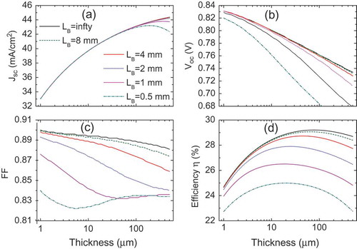
To appreciate the effect of SRH recombination, in we show ,
, FF, and the efficiency
with the same parameters as those of , but reducing the diffusion length of minority carriers in the base (
in the dark, as discussed above) from
to LB = 500 µm. The maximum efficiency is reduced from 29.2% to 25% and the optimal thickness is decreased from 80 to 20 µm. A more complete analysis of the optimal thickness for a given material quality also in the presence of parasitic losses, and of the requirements to reach a given efficiency target, is given in Ref. [Citation102]. Notice that the short-circuit current is unchanged, unless the diffusion length becomes comparable to or smaller than the cell thickness. The open-circuit voltage and the FF, instead, are much more strongly affected by a reduction in the diffusion length. Comparing with the record HJ-IBC solar cell parameters [Citation6] shown in , we can estimate the diffusion length in the dark to be larger than at least 4 mm. The minority carrier lifetime in the base,
, must be larger than ~10 ms, which agrees well with direct measurements [Citation6].
Figure 7. Effect of Shockley–Read–Hall recombination, expressed by the diffusion length, , for different absorber thicknesses. Other parameters are the same as in . Results are calculated with the generalized Hovel model.
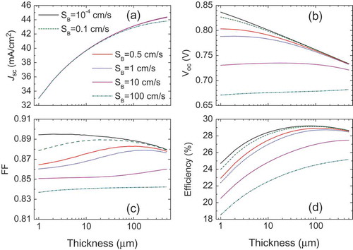
The results of and are calculated in the absence of surface recombination. Surprisingly, the maximum efficiency is found to be very sensitive to surface recombination even at very small levels. To show this point, in we show ,
, the FF, and the efficiency η for different values of the SRV at the rear surface. It can be seen that both
and FF are strongly affected by surface recombination, even at values below S = 1 cm/s. The effect is largest at small thicknesses, which is physically intuitive, as the role of surfaces is expected to become more important for thinner samples. However the effect of surface recombination is nonnegligible at any thickness: for example, assuming
cm/s leads to a maximum efficiency
% [Citation102]. The reason for this high sensitivity to surface recombination lies in the fact that c-Si solar cells close to the efficiency limits are in the high-injection regime, in which the photogenerated carrier density becomes larger than the doping. This regime is characterized by an unusually high concentration of photogenerated carriers, which accumulate at the interfaces and are more subject to surface recombination. A full account of surface recombination in this regime requires simulations with the FEM method. Nevertheless, it should be said that silicon solar cells must be very close to ideal conditions for the high-injection regime to occur. Moreover, the limit of vanishing SRV (
) is an idealized one that is never approached in practice. The record SRV value measured on silicon surfaces is ~0.2 cm/s [Citation103], typical values for the Si/SiO2 interface are around 1 cm/s, and passivation of complex morphological structures by atomic-layer deposition is considered to be very good when it reaches ~10 cm/s [Citation104].
Figure 8. Effect of surface recombination, expressed by the surface recombination velocity at the rear surface, for different absorber thicknesses. Other parameters are the same as in . Results are calculated with the finite-element method.
The current record efficiency % of c-Si solar cells [Citation6,Citation7] is already very close to the limiting value of ~29%, and some further increase is expected in the near future [Citation6]. Also, the module efficiency (which has by now a record value of ~24.4% in the lab and ~21% in the market [Citation1]) has still margins for improvements, which are expected to contribute to further reduction of the cost of PV power in the coming years [Citation8]. Yet, these are incremental improvements on the line of the existing technology of single-junction solar cells, and they are eventually bound by the ~29% limit.
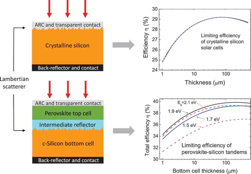
Breakthrough improvements of silicon PVs beyond this limit can come from the concept of tandem solar cells, i.e. by adding a second solar cell with a higher bandgap material on top of the high-efficiency c-Si cell. In the last 5 years, exciting progress has been made with so-called perovskite solar cells, which are usually based on the methylammonium-lead-halide (MALI) material with a perovskite structure [Citation105,Citation106]. In ), we show the schematic structure of a silicon/perovskite tandem. We consider a four-terminal configuration, i.e. the two solar cells are assumed to be electrically independent. In ), we show the calculated efficiency limits (we model the top perovskite cell by the diode equation and the bottom silicon cell by the generalized Hovel model, see Ref. [Citation98] for details) when the perovskite bandgap is changed from 1.5 eV (the typical value for MALI) to 2.1 eV. The efficiency limit is nearly 40%; it occurs for a silicon thickness in the range 100–300 µm and a perovskite bandgap between 1.8 and 2 eV. This value can be compared with the detailed-balance limit for an unconstrained two-cell tandem, which is 45.7% [Citation107,Citation108]. The present ~40% limit is lower because the value of the silicon bandgap is slightly higher than the optimal one for the bottom cell, and because of Auger recombination in silicon. In any case, these results confirm that silicon/perovskite tandems have the potential for drastically improving the efficiency of silicon-based solar cells over current values. However, actual realization of this possibility will depend on materials science progress related to perovskite solar cells to solve the crucial issues of proper bandgap, long-term stability, and toxicity due to Pb content. A detailed study of the efficiency limits of perovskite/silicon tandems is presented in Ref. [Citation109], and a recent review of this hot area is given in Ref. [Citation110].
Figure 9. (a) Scheme of the silicon/perovskite tandem solar cell. (b) Efficiency of the tandem as a function of the thickness of the silicon bottom cell, calculated for different values of the perovskite bandgap. Adapted from Ref. [Citation98], with permission from IOP Publishing. Inset: maximum efficiency as a function of perovskite gap.
![Figure 9. (a) Scheme of the silicon/perovskite tandem solar cell. (b) Efficiency of the tandem as a function of the thickness of the silicon bottom cell, calculated for different values of the perovskite bandgap. Adapted from Ref. [Citation98], with permission from IOP Publishing. Inset: maximum efficiency as a function of perovskite gap.](/cms/asset/ee79168f-96c0-4a2e-b5d1-f590d160a104/tapx_a_1548305_f0009_oc.jpg)
Another possibility for improving upon the efficiency of single-junction silicon solar cells is that of III-V/silicon multijunctions. Recently, a III-V/Si triple-junction solar cell with 30.2% efficiency has been fabricated by means of wafer bonding of two independently prepared c-Si and GaInP/AlGa
As solar cells [Citation111]. The efficiency rises to 32.8% for mechanically stacked (independently operated) III-V/Si double junctions, and to 35.9% for triple junctions [Citation112]. Although the cost of epitaxial III-V materials represents an obstacle to industrial exploitation, these benchmark results confirm the potential of multijunction structures to overcome the efficiency limits of single-junction c-Si cells.
5. Conclusions
We have discussed theoretical approaches for calculating the conversion efficiency of solar cells, focusing on single-junction c-Si devices. For what concerns the optical part (i.e. the spectral absorptance and the photogeneration profile), the indirect gap of silicon imposes the use of proper light-trapping structures to enhance the optical path of light in the material. However, optimal light trapping can hardly exceed the Lambertian limit as provided by a random scatterer, except in narrow spectral or angular ranges. The short-circuit current – i.e. the integrated absorptance weighted with the solar spectrum – approaches the maximum value for thicknesses larger than several 10 µm. Micron-size c-Si solar cells (i.e. whose thickness is of the order of the wavelength of visible light) are interesting as they operate in the nanophotonic limit; however, their efficiency cannot compete with that of thick (wafer-based, >100 µm thick) devices.
For what concerns the electrical part of the problem (i.e. the collection of photogenerated carriers), we have discussed three different approaches, namely the ideal diode equation, an analytic model for solving drift-diffusion equations in 1-D (the generalized Hovel model), and full device simulations with the FEM. We have shown that it is possible to combine rigorous optical calculations of a randomly rough interface with full electrical simulations by the FEM method. Analytic approaches to the electrical calculations are also possible and are in good agreement with the full simulations. This allows to describe c-Si solar cells in a wide range of thicknesses, from ~1 µm to several 100 µm, taking into account the effects of bulk and surface recombination. The optimal values of silicon thicknesses – for material parameters that correspond to non-wafer-based silicon – lie in the range 20–100 µm, depending on material quality.
The efficiency limits of c-Si solar cells can be calculated by assuming Lambertian light trapping and by neglecting defect-related recombinations. The limiting efficiency including Auger recombination is ~29% and it occurs for 80-µm thickness, with a broad maximum. The three approaches to the electronic transport properties agree well with each other as long as surface recombination is neglected. The maximum efficiency may occur under high-injection conditions, i.e. when the density of photogenerated carriers is much larger than the doping: in this peculiar situation, the efficiency is highly sensitive to surface recombination even at very small levels, and this effect can be rigorously calculated only with the full FEM approach. However, under normal (experimentally realized) conditions, the generalized Hovel model gives a very good description of silicon solar cells as a function of thickness, including the effects of bulk and surface recombinations. Improving the efficiency of silicon-based solar cells beyond the 29% limit requires the use of tandem structures, which potentially have a much higher (~40%) efficiency limit. Both perovskite/silicon and III-V/silicon multijunctions are of great interest in this respect.
Continuous cost reduction and efficiency improvements of silicon solar cells will be crucial in order to increase the share of PV electricity in the energy mix in the coming years. While silicon solar cells are approaching the efficiency limits, margins of improvement are still present and will be undoubtedly implemented both in the lab and in industrial processes. Breakthrough improvements with silicon tandems are more prospective and are still the focus of intense lab research. Cross-disciplinary research combining physics, chemistry, materials science, engineering, and economics will be a key for short- and long-term progress in the field.
Disclosure statement
No potential conflict of interest was reported by the authors.
Additional information
Funding
References
- Fraunhofer ISE Photovoltaics Report (12 July 2017), available at https://www.ise.fraunhofer.de/en/publications/studies/photovoltaics-report.html
- European Commission - JRC, PV Status Report 2017 (10 November 2017), available at https://ec.europa.eu/jrc/en/publication/eur-scientific-and-technical-research-reports/pv-status-report-2017
- J.H. Zhao, A. Wang and M. Green, Progr. Photov.: Res. Appl. 7 (1999) pp. 125–148. doi:10.1002/(SICI)1099-159X(199911/12)7:6<471::AID-PIP298>3.0.CO;2-7
- M.A. Green, Progr. Photov.: Res. Appl. 17 (2009) pp. 183–189. doi:10.1002/pip.892
- K. Masuko, M. Shigematsu, T. Hashiguchi, D. Fujishima, M. Kai, N. Yoshimura, T. Yamaguchi, Y. Ichihashi, T. Mishima, N. Matsubara, T. Yamanishi, T. Takahama, M. Taguchi, E. Maruyama and S. Okamoto, IEEE J. Photovoltaics. 4 (2014) pp. 1433–1435. doi:10.1109/JPHOTOV.2014.2352151
- K. Yoshikawa, H. Kawasaki, W. Yoshida, T. Irie, K. Konishi, K. Nakano, T. Uto, D. Adachi, M. Kanematsu, H. Uzu and K. Yamamoto, Nat. Energy. 2 (2017) pp. 17032 (8pp). doi:10.1038/nenergy.2017.32
- M.A. Green, Y. Hishikawa, E.D. Dunlop, D.H. Levi, J. Hohl-Ebinger and A.W. Ho-Baillie, Progr. Photov Res. Appl. 26 (2018) pp. 3–12. doi:10.1002/pip.2978
- International Technology Roadmap for Photovoltaic, available at http://www.itrpv.net/
- W. Shockley and H.J. Queisser, J. Appl. Phys. 32 (1961) pp. 510–519. doi:10.1063/1.1736034
- T. Tiedje, E. Yablonovitch, G.D. Cody and B.G. Brooks, IEEE Trans. Electron Devices. 31 (1984) pp. 711–716. doi:10.1109/T-ED.1984.21594
- M.A. Green, IEEE Trans. Electron. Devices. 31 (1984) pp. 671–678. doi:10.1109/T-ED.1984.21588
- M.A. Green, Progr. Photov.: Res. Appl. 7 (1999) pp. 327–330. doi:10.1002/(SICI)1099-159X(199907/08)7:4<327::AID-PIP250>3.0.CO;2-B
- M.J. Kerr, A. Cuevas and P. Campbell, Progr. Photov.: Res. Appl. 11 (2003) pp. 97–104. doi:10.1002/pip.464
- A. Richter, M. Hermle and S.W. Glunz, IEEE J. Photov. 3 (2013) pp. 1184–1191. doi:10.1109/JPHOTOV.2013.2270351
- R. Swanson, Thirty-First IEEE Photovoltaic Specialists Conference. (2005) pp. 889–894. doi: 10.1109/PVSC.2005.1488274
- E. Yablonovitch, J. Opt. Soc. Am. 72 (1982) pp. 899–907. doi:10.1364/JOSA.72.000899
- E. Yablonovitch and G.D. Cody, IEEE Trans. Electron. Dev. 29 (1982) pp. 300–305. doi:10.1109/T-ED.1982.20700
- M.A. Green, Progr. Photov.: Res. Appl. 10 (2002) pp. 235–241. doi:10.1002/pip.404
- M.A. Green, Sol. Energy Mater. Sol. Cells. 92 (2008) pp. 1305–1310. doi:10.1016/j.solmat.2008.06.009
- C.S. Schuster, P. Kowalczewski, E.R. Martins, M. Patrini, M.G. Scullion, M. Liscidini, L. Lewis, C. Reardon, L.C. Andreani and T.F. Krauss, Opt. Express. 21 (2013) pp. A433–A439. doi:10.1364/OE.21.017108
- E. Palik, Handbook of Optical Constants of Solids, Academic Press, London, 1985.
- M.I. Alonso, M. Garriga, C. Durante Rincón, E. Hernández and M. Léon, Appl. Phys. A. 74 (2002) pp. 659–664. doi:10.1007/s003390100931
- A. Bozzola, M. Liscidini and L.C. Andreani, Opt. Express. 20 (2012) pp. A224–A244. doi:10.1364/OE.20.00A224
- Notice that Jsc for c-Si keeps increasing even for thicknesses larger than 103 or even 104 µm. This is due to sub-bandgap absorption, which goes to zero slowly below 1.12 eV (i.e., in the wavelength range ~1000–1200 nm). The precise behavior of Jsc at large thicknesses depends on the detailed form of the dielectric functions below the bandgap [19], however it is unimportant as the interesting range of thicknesses for high efficiency is below a few 100 µm.
- J. Nelson, The Physics of Solar Cells, Imperial College Press, London, 2003.
- A. Smets, K. Jäger, O. Isabella, R. Van Swaaij and M. Zeman, Solar Energy, UIT Cambridge, England, 2016.
- A. Bozzola, P. Kowalczewski and L.C. Andreani, J. Appl. Phys. 115 (2014) pp. 094501. doi:10.1063/1.4867008
- C. Heine and R.H. Morf, Appl. Opt. 34 (1995) pp. 2476–2482. doi:10.1364/AO.34.002476
- S. Hava and M. Auslender, Sol. Energy Mater. Sol. Cells. 61 (2000) pp. 143–151. doi:10.1016/S0927-0248(99)00107-5
- P. Bermel, C. Luo, L. Zeng, L.C. Kimerling and J.D. Joannopoulos, Opt. Express. 15 (2007) pp. 16986–17000.
- A. Chutinan and S. John, Phys. Rev. A. 78 (2008) doi:10.1103/PhysRevA.78.023825
- C. Ulbrich, M. Peters, B. Blaesi, T. Kirchartz, A. Gerber and U. Rau, Opt. Express. 18 (2010) pp. A133–A138. doi:10.1364/OE.18.025008
- S. Zanotto, M. Liscidini and L.C. Andreani, Opt. Express. 18 (2010) pp. 4260–4272. doi:10.1364/OE.18.025008
- K.X. Wang, Z. Yu, V. Liu, Y. Cui and S. Fan, Nano Lett. 12 (2012) pp. 1616–1619. doi:10.1021/nl204550q
- V. Depauw, X. Meng, O. El Daif, G. Gomard, L. Lalouat, E. Drouard, C. Trompoukis, A. Fave, C. Seassal and I. Gordon, IEEE J. Photov. 4 (2014) pp. 215–223. doi:10.1109/JPHOTOV.2013.2286521
- J. Buencuerpo, L.E. Munioz-Camuniez, M.L. Dotor and P.A. Postigo, Opt. Express. 20 (2012) pp. A452–A464. doi:10.1364/OE.20.00A452
- X. Meng, V. Depauw, G. Gomard, O.E. Daif, C. Trompoukis, E. Drouard, C. Jamois, A. Fave, F. Dross, I. Gordon and C. Seassal, Opt. Express. 20 (2012) pp. A465–A475. doi:10.1364/OE.20.00A465
- X. Meng, E. Drouard, G. Gomard, R. Peretti, A. Fave and C. Seassal, Opt. Express. 20 (2012) pp. A560–A571. doi:10.1364/OE.20.00A560
- M. Peters, C. Battaglia, K. Forberich, B. Blaesi, N. Sahraei and A.G. Aberle, Opt. Express. 20 (2012) pp. 29488–29499. doi:10.1364/OE.20.029488
- F.J. Haug, K. Söderström, A. Naqavi, J. Li and C. Ballif, Appl. Phys. Lett. 103 (2013) pp. 131108. doi:10.1063/1.4822105
- G. Gomard, R. Peretti, E. Drouard, X. Meng and C. Seassal, Opt. Express. 21 (2013) pp. A515–A527. doi:10.1364/OE.21.017108
- O. Isabella, S. Solntsev, D. Caratelli and M. Zeman, Progr. Photov.: Res. Appl. 21 (2013) pp. 94–108. doi:10.1002/pip.1257
- S. Eyderman, S. John and A. Deinega, J. Appl. Phys. 113 (2013) pp. 154315 (11pp). doi:10.1063/1.4802442
- A. Deinega, S. Eyderman and S. John, J. Appl. Phys. 113 (2013) pp. 224501 (9pp). doi:10.1063/1.4809982
- J. Eisenlohr, J. Benick, M. Peters, B. Blaesi, J.C. Goldschmidt and M. Hermle, Opt. Express. 22 (2014) pp. A111–A119. doi:10.1364/OE.22.00A111
- K.X. Wang, Z. Yu, V. Liu, A. Raman, Y. Cui and S. Fan, Energy Environ. Sci. 7 (2014) pp. 2725–2738. doi:10.1039/C4EE00839A
- S. Eyderman, S. John, M. Hafez, S.S. Al-Ameer, T.S. Al-Harby, Y. Al-Hadeethi and D.M. Bouwes, J. Appl. Phys. 118 (2015) pp. 023103 (7pp). doi:10.1063/1.4926548
- J. Eisenlohr, N. Tucher, H. Hauser, M. Graf, J. Benick, B. Blaesi, J.C. Goldschmidt and M. Hermle, Sol. Energy Mater. Sol. Cells. 155 (2016) pp. 288–293. doi:10.1016/j.solmat.2016.06.033
- Y. Tanaka, K. Ishizaki, M.D. Zoysa, T. Umeda, Y. Kawamoto, S. Fujita and S. Noda, Progr. Photov.: Res. Appl. 23 (2015) pp. 1475–1483. doi:10.1002/pip.2577
- M. De Zoysa, K. Ishizaki, Y. Tanaka, H. Sai, K. Matsubara and S. Noda, Appl. Phys. Express. 10 (2017) doi:10.7567/APEX.10.012302
- K. Ishizaki, A. Motohira, M. De Zoysa, Y. Tanaka, T. Umeda and S. Noda, IEEE J. Photovoltaics. 7 (2017) pp. 950–956. doi:10.1109/JPHOTOV.2017.2695524
- O. Isabella, J. Krc and M. Zeman, Appl. Phys. Lett. 97 (2010) pp. 101106 (3pp). doi:10.1063/1.3488023
- A. Ingenito, O. Isabella and M. Zeman, Progr. Photov.: Res. Appl. 23 (2015) pp. 1649–1659. doi:10.1002/pip.2606
- H. Tan, E. Moulin, F.T. Si, J.W. Schuettauf, M. Stuckelberger, O. Isabella, F.J. Haug, C. Ballif, M. Zeman and A.H.M. Smets, Progr. Photov.: Res. Appl. 23 (2015) pp. 949–963. doi:10.1002/pip.2639
- O. Isabella, R. Vismara, A. Ingenito, N. Rezaei and M. Zeman, Opt. Express. 24 (2016) pp. A708–A719. doi:10.1364/OE.24.029465
- S. Fahr, T. Kirchartz, C. Rockstuhl and F. Lederer, Opt. Express. 19 (2011) pp. A865– A874. doi:10.1364/OE.19.00A865
- C. Battaglia, C.M. Hsu, K. Söderström, J. Escarré, F.J. Haug, M. Charriére, M. Boccard, M. Despeisse, D.T.L. Alexander, M. Cantoni, Y. Cui and C. Ballif, ACS Nano. 6 (2012) pp. 2790–2797. doi:10.1021/nn300287j
- K. Vynck, M. Burresi, F. Riboli and D.S. Wiersma, Nat. Mater. 11 (2012) pp. 1017–1022. doi:10.1038/nmat3442
- P. Kowalczewski, M. Liscidini and L.C. Andreani, Opt. Lett. 37 (2012) pp. 4868–4870. doi:10.1364/OL.37.002250
- P. Kowalczewski, M. Liscidini and L.C. Andreani, Opt. Express. 21 (2013) pp. A808–A820. doi:10.1364/OE.21.017108
- M. Burresi, F. Pratesi, K. Vynck, M. Prasciolu, M. Tormen and D.S. Wiersma, Opt. Express. 21 (2013) pp. A268–A275. doi:10.1364/OE.21.017108
- S. Wiesendanger, M. Zilk, T. Pertsch, F. Lederer and C. Rockstuhl, Appl. Phys. Lett. 103 (2013) pp. 131115. doi:10.1063/1.4823554
- A. Oskooi, M. De Zoysa, K. Ishizaki and S. Noda, ACS Photonics. 1 (2014) pp. 304–309. doi:10.1021/ph400140f
- A. Ingenito, O. Isabella and M. Zeman, ACS Photonics. 1 (2014) pp. 270–278. doi:10.1021/ph4001586
- C. Trompoukis, I. Abdo, R. Cariou, I. Cosme, W. Chen, O. Deparis, A. Dmitriev, E. Drouard, M. Foldyna, E. Garcia-Caurel, I. Gordon, B. Heidari, A. Herman, L. Lalouat, K.D. Lee, J. Liu, K. Lodewijks, F. Mandorlo, I. Massiot, A. Mayer, V. Mijkovic, J. Muller, R. Orobtchouk, G. Poulain, P. Prod’Homme, P. Roca I Cabarrocas, C. Seassal, J. Poort-Mans, R. Mertens, O. El Daif and V. Depauw, Phys. Status Solidi A Appl. Mat. Sci. 212 (2015) pp. 140–155. doi:10.1002/pssa.201431180
- C. Trompoukis, I. Massiot, V. Depauw, O.E. Daif, K. Lee, A. Dmitriev, I. Gordon, R. Mertens and J. Poortmans, Opt. Express. 24 (2016) pp. A191–A201. doi:10.1364/OE.24.029465
- A. Gaucher, A. Cattoni, C. Dupuis, W. Chen, R. Cariou, M. Foldyna, L. Laloua, E. Drouard, C. Seassal, P. Roca I Cabarrocas and S. Collin, Nano Lett. 16 (2016) pp. 5358–5364. doi:10.1021/acs.nanolett.6b01240
- L. Lalouat, H. Ding, B. Gonzalez-Acevedo, A. Harouri, R. Orobtchouk, V. Depauw, E. Drouard and C. Seassal, Sol. Energy Mater. Sol. Cells. 159 (2017) pp. 649–656. doi:10.1016/j.solmat.2016.04.031
- V. Jovanov, E. Moulin, F.J. Haug, A. Tamang, S.I.H. Bali, C. Ballif and D. Knipp, Sol. Energy Mater. Sol. Cells. 160 (2017) pp. 141–148. doi:10.1016/j.solmat.2016.10.005
- E.R. Martins, J. Li, Y. Liu, V. Depauw, Z. Chen, J. Zhou and T.F. Krauss, Nat. Commun. 4 (2013) pp. 2665. doi:10.1038/ncomms3665
- F. Pratesi, M. Burresi, F. Riboli, K. Vynck and D.S. Wiersma, Opt. Express. 21 (2013) pp. A460–A468. doi:10.1364/OE.21.017108
- A. Bozzola, M. Liscidini and L.C. Andreani, Prog. Photovolt. 22 (2014) pp. 1237–1245.
- S. John, Nat. Mater. 11 (2012) pp. 997–999. doi:10.1038/nmat3503
- C.S. Schuster, A. Bozzola, L.C. Andreani and T.F. Krauss, Opt. Express. 22 (2014) pp. A542–A551. doi:10.1364/OE.22.00A542
- F. Priolo, T. Gregorkiewicz, M. Galli and T.F. Krauss, Nat. Nanotechnol. 9 (2014) pp. 19–32. doi:10.1038/nnano.2013.271
- M. Burresi, F. Pratesi, F. Riboli and D.S. Wiersma, Adv. Opt. Mat. 3 (2015) pp. 722–743. doi:10.1002/adom.201400514
- C.S. Schuster, S. Morawiec, M.J. Mendes, M. Patrini, E.R. Martins, L. Lewis, I. Crupi and T.F. Krauss, Optica. 2 (2015) pp. 194–200. doi:10.1364/OPTICA.2.000194
- C.S. Schuster, Diffractive Optics for Thin-Film Silicon Solar Cells, Springer Theses, Springer International Publishing AG, Switzerland, 2017.
- Z. Yu, A. Raman and S. Fan, Proc. Natl. Acad. Sci. U.S.A. 107 (2010) pp. 17491–17496. doi:10.1073/pnas.1008296107
- Z. Yu, A. Raman and S. Fan, Opt. Express. 18 (2010) pp. A366–A380. doi:10.1364/OE.18.025008
- Z. Yu, A. Raman and S. Fan, Appl. Phys. A Mater. Sci. Process. 105 (2011) pp. 329–339. doi:10.1007/s00339-011-6617-4
- Z. Yu and S. Fan, Appl. Phys. Lett. 98 (2011) pp. 011106. doi:10.1063/1.3532099
- Z. Yu, A. Raman and S. Fan, Phys. Rev. Lett. 109 (2012) pp. 173901. doi:10.1103/PhysRevLett.109.173901
- A. Naqavi, F.J. Haug, C. Battaglia, H.P. Herzig and C. Ballif, J. Opt. Soc. Am. B. 30 (2013) pp. 13–20. doi:10.1364/JOSAB.30.000013
- S. Buddhiraju and S. Fan, Phys. Rev. B. 96 (2017) pp. 035304. doi:10.1103/PhysRevB.96.035304
- A. Bozzola, P. Kowalczewski and L.C. Andreani, J. Appl. Phys. 117 (2015) pp. 026102. doi:10.1063/1.4905183
- P. Kowalczewski, A. Bozzola, M. Liscidini and L.C. Andreani, J. Appl. Phys. 115 (2014) pp. 194504. doi:10.1063/1.4876223
- L.C. Andreani, A. Bozzola, P. Kowalczewski and M. Liscidini, Sol. Energy Mater. Sol. Cells. 135 (2015) pp. 78–92. doi:10.1016/j.solmat.2014.10.012
- Silvaco-ATLAS, Available at https://www.silvaco.com/products/tcad/device.simulation/atlas/atlas.html
- J.H. Petermann, D. Zielke, J. Schmidt, F. Haase, E.G. Rojas and R. Brendel, Progr. Photov.: Res. Appl. 20 (2012) pp. 1–5. doi:10.1002/pip.1129
- M.S. Branham, W.C. Hsu, S. Yerci, J. Loomis, S.V. Boriskina, B.R. Hoard, S.E. Han and G. Chen, Adv. Mater. 27 (2015) pp. 2182–2188. doi:10.1002/adma.201405511
- H.S. Radhakrishnan, R. Martini, V. Depauw, K. Van Nieuwenhuysen, T. Bearda, I. Gordon, J. Szlufcik and J. Poortmans, Sol. Energy Mater. Sol. Cells. 135 (2015) pp. 113–123. doi:10.1016/j.solmat.2014.10.049
- R. Cariou, W. Chen, I. Cosme-Bolanos, J.L. Maurice, M. Foldyna, V. Depauw, G. Patri-Arche, A. Gaucher, A. Cattoni, I. Massiot, S. Collin, E. Cadel, P. Pareige and P. Roca I Cabarrocas, Progr. Photov.: Res. Appl. 24 (2016) pp. 1075–1084. doi:10.1002/pip.2762
- G. Koeppel, D. Amkreutz, P. Sonntag, G. Yang, R. Van Swaaij, O. Isabella, M. Zeman, B. Rech and C. Becker, IEEE J. Photov. 7 (2017) pp. 85–90. doi:10.1109/JPHOTOV.2016.2618605
- C. Gemmel, J. Hensen, S. Kajari-Schroeder and R. Brendel, IEEE J. Photov. 7 (2017) pp. 430–436. doi:10.1109/JPHOTOV.2016.2642640
- A. Richter, S.W. Glunz, F. Werner, J. Schmidt and A. Cuevas, Phys. Rev. B. 86 (2012) pp. 165202. doi:10.1103/PhysRevB.86.165202
- A. Schenk, J. Appl. Phys. 84 (1998) pp. 3684–3695. doi:10.1063/1.368545
- P. Kowalczewski, L. Redorici, A. Bozzola and L.C. Andreani, J. Opt. 18 (2016) pp. 054001 (11 pp). doi:10.1088/2040-8978/18/5/054001
- H.J. Hovel, Semiconductors and Semimetals. Solar Cells, Vol. 11, Academic, New York, 1975.
- https://github.com/kowalczewski/Lisa
- P.P. Altermatt, A. Schenk, F. Geelhaar and G. Heiser, J. Appl. Phys. 93 (2003) pp. 1598–1604. doi:10.1063/1.1529297
- P. Kowalczewski and L.C. Andreani, Sol. Energy. Mater. Sol. Cells. 143 (2015) pp. 60–268. doi:10.1016/j.solmat.2015.06.054
- E. Yablonovitch, D.L. Allara, C.C. Chang, T. Gmitter and T.B. Bright, Phys. Rev. Lett. 57 (1986) pp. 249–252. doi:10.1103/PhysRevLett.57.1324
- M. Otto, M. Kroll, T. Käsebier, R. Salzer, A. Tünnermann and R.B. Wehrspohn, Appl. Phys. Lett. 100 (2012) pp. 191603. doi:10.1063/1.4714546
- M. Grätzel, Nat. Mater. 13 (2014) pp. 838–842. doi:10.1038/nmat4065
- W. Zhang, G.E. Eperon and H.J. Snaith, Nat. Energy. 1 (2016) pp. 16048 (5pp).
- A.S. Brown and M.A. Green, Physica E. 14 (2002) pp. 96–100. doi:10.1016/S1386-9477(02)00364-8
- M. Green, Third-Generation Photovoltaics, Springer, Berlin, 2003.
- M.H. Futscher and B. Ehrler, ACS Energy Lett. 1 (2016) pp. 863–868. doi:10.1021/acsenergylett.6b00405
- J. Werner, B. Niesen and C. Ballif, Adv. Mater. Interfaces. (2017) doi:10.1002/admi.201700731
- R. Cariou, J. Benick, P. Beutel, N. Razek, C. Floetgen, M. Hermle, D. Lackner, S.W. Glunz, A.W. Bett, M. Wimplinger and F. Dimroth, IEEE J. Photov. 7 (2017) pp. 367–373. doi:10.1109/JPHOTOV.2016.2629840
- S. Essig, C. Allebé, T. Remo, J. Geisz, M. Steiner, K. Horowitz, L. Barraud, J. Ward, M. Schnabel, A. Descoeudres, D. Yound, M. Woodhouse, M. Despeisse, C. Ballif and A. Tamboli, Nat. Energy. 2 (2017) pp. 17144 (9pp). doi:10.1038/nenergy.2017.144