
ABSTRACT
In this article, we discuss the recent progress on controlled structural modification of 2D materials by means of molecular functionalization, with a focus on scanning probe microscopy techniques for their characterization. For many practical applications of these novel materials, it is necessary to tune their electronic and optical properties, and molecule-based functionalization is a powerful approach to reach this. We discuss recent covalent and non-covalent approaches, for functionalization of graphene, transition metal dichalcogenides, black phosphorus, and hexagonal boron nitride. Nanostructuring approaches and their impact on 2D materials’ properties are highlighted.
Graphical abstract
Past decades have witnessed advancement in material science beginning from experimental revelations of novel properties of graphene, a material which was earlier considered as thermodynamically unstable at finite temperature. Remarkably high electron mobility of 2.0 × 105 cm2 V−1 s−1 at room temperature [Citation1], 1TPa of Young’s modulus, along with high flexibility lead to potential applications in touch screens, capacitors, spintronic devices, fuel cells, batteries, sensors, transparent conductive films, high-frequency circuits, toxic material removal, and flexible electronics. A limitation of graphene arises from the Dirac-like linear dispersion, which on the one hand limits the range of applications due to the absence of a band gap, but on the other hand, can lead to unexpected physics with a lot of fascinating properties to explore. Thus, it was soon realized that tuning the electronic band structure of this material is an important target. For this purpose different methods to functionalize graphene by chemisorbed or physisorbed molecules [Citation2–Citation5], substitutional doping [Citation6], intercalation of molecules [Citation7] and metal atoms, and other reactions such as hydrogenation and fluorination were explored.
Modifications of graphene by physisorbed organic molecules or chemisorption of reactive molecules via covalent bonds have resulted in the overall modification of the electronic properties of graphene. Functionalization of graphene by physisorbed molecules (randomly adsorbed or self-assembled) has been shown to induce n-type or p-type doping. Due to the presence of delocalized π electrons, graphene is highly susceptible to adsorbates on the surface. Therefore, organic molecules with the highest occupied molecular orbital (HOMO) and lowest unoccupied molecular orbital (LUMO) at a suitable position with respect to Fermi level of graphene can be used to dope graphene [Citation8,Citation9]. Chemisorption of reactive molecules occurs via formation of covalent bonds between graphene carbon atoms and molecules, resulting in transforming sp2 carbon atoms of graphene in sp3 carbon atoms at the site of molecule attachment [Citation9,Citation10]. Chemisorption of molecules is more stable when compared to physisorption but at the same time can cause detrimental effects on the novel properties of graphene. Covalent functionalization of graphene is considered as the best possible way to robustly modify the electronic band structure of graphene thus promoting its application in future nanoelectronic devices. For covalent functionalization of graphene different organic functional groups such as diazonium [Citation10–Citation12], and maleimide [Citation13] have been used. Among these, covalent functionalization using diazonium chemistry is most thoroughly studied.
The growth of graphene research has led to exploring other layered 2D inorganic materials such as transition metal dichalcogenides (TMDs), black phosphorus, and hexagonal boron nitride. These can be thinned down to monolayers. The atomically thin nature of these materials results in unique structural and physical properties and provides access to novel fundamental properties which are not present in their bulk counterparts. Synthetic methods such as vapor phase methods, wet chemical synthesis, and liquid phase exfoliation are the most prominent methods for growth of 2D TMDs [Citation14,Citation15]. Bulk TMDs have found applications in energy conversion and storage. The electronic band structure is what makes TMDs interesting, whereby the bandgap of TMDs is highly dependent on the number of layers in a TMD stack and also on the constituent atoms as well as the coordination of these materials [Citation16], which is a basic fundamental property not found in graphene. The combination of atomic scale thickness, layer dependent electronic band structure, strong spin-orbit coupling, and superior mechanical properties makes these materials interesting for applied as well as fundamental research.
However, for developing practical and reliable high performance (opto)-electronic devices based on 2D TMDs, a controlled tuning of their electronic properties is necessary. Doping of 2D TMDs is important for minimizing the Schottky barrier at the interface of the TMD and metal contact to reduce the charge carrier recombination rate at the interface. Conventional methods of doping such as ion implantation and substitutional doping are not suitable for 2D TMDs as they can create defects in the layer, having a negative impact on the electronic properties. A number of different approaches have been proposed to overcome this hurdle which are discussed in a recent review on doping engineering of TMDs by different methods [Citation17]. Among these approaches, the most promising are the ones involving physisorption and chemisorption of organic molecules with functional groups having strong interactions with the TMD layers.
Charge transfer interactions and dipolar interactions are two prominent factors that can result in doping of TMDs. Charge transfer doping is mostly dependent on the redox potential of molecules with respect to the Fermi level of TMDs, whereas molecules on TMDs with dipolar interactions create an electric field that modulates the local charge carrier density of TMDs. Creating interfaces of TMDs with molecules can, therefore, improve the device performance characteristics by controlling the doping (n-type or p-type). Self-assembly of molecules with fixed a dipole can create a non-zero field, therefore, creating macroscopic changes to the (opto)-electronic properties of TMDs.
In addition to physisorption, also chemisorption approaches are very promising. A lot of focus has been devoted towards improving the dispersibility of TMDs in solutions by covalent functionalization with molecules to develop methods for large area processing of TMDs. Covalent functionalization of MoS2, the most popular TMD, has been carried out by number of approaches such as thiol addition [Citation18–Citation24], addition of dibenzene thiophene [Citation25], aryl diazonium molecules [Citation26,Citation27] and organohalides [Citation28,Citation29]. Pristine MoS2, either CVD grown or chemically exfoliated, always has structural defects in the form of sulfur vacancy sites along with other point defects. These defects act as scattering centers for the majority of charge carriers in MoS2. Covalent functionalization by sulfur containing groups or diazonium groups can result in passivating the surface defects by grafting at such defect sites. Additionally, for 2D TMDs covalent functionalization is a facile and robust method of doping compared to traditional ion-implantation methods. Molecular chemistry approaches for covalent and well as non-covalent functionalization of TMDs is comprehensively reviewed by Bertolazzi et al. [Citation30].
In this review, we will focus on recent work on non-covalent and covalent functionalization of substrate-supported graphene and other 2D materials, which result in a modulation of their properties. We mostly focus on recent work that involves the use of scanning probe microscopy (SPM) based techniques to visualize the supramolecular assemblies as well as covalently grafted molecules on the 2D material. SPM techniques provide access to sub-nanometer level resolution, thus, any change in the molecular and 2D material properties upon interaction with the 2D material can be directly visualized. We demonstrate that SPM-based methods, such as Kelvin probe force microscopy (KPFM) and scanning tunneling spectroscopy (STS), can give insight into the charge transfer interactions between molecules and the 2D material. In section 1, the impact and importance of primarily self-assembled molecular layers are discussed. Covalent functionalization is discussed in section 2.
Non-covalent functionalization of 2D materials
Given the ultrathin nature of 2D materials, surface functionalization using molecular species is a promising approach for tuning the properties of these materials. Non-covalent functionalization of 2D materials provides a way to tune the electronic and physical properties without disrupting crystal structure. Physisorbed molecules interact with 2D materials via van der Waals (vdW) interactions or electrostatic forces, which can be used to controllably tune doping levels. Non-covalent functionalization of 2D materials can be carried out by physisorbed molecules, forming self-assembled structures or adsorbing randomly on the top (or bottom) surface of the 2D material.
Self-assembly of organic molecules on highly oriented pyrolytic graphite (HOPG) into self-assembled molecular networks (SAMNs) [Citation31], which can be considered as a model system for molecular assembly on graphene, has been thoroughly studied experimentally and theoretically, resulting in a good understanding of molecular self-assembly on planar surfaces. Similarly, functionalization by SAMNs is being considered a promising approach for other 2D materials. In the case of graphene, a number of reviews published in the past few years have summarized different approaches towards non-covalent functionalization by self-assembled molecules [Citation2–Citation5].
Thus, for graphene, we will only focus on recent studies on the non-covalent functionalization with molecules leading to a charge transfer. Charge transfer interactions result in a redistribution of electrons between the molecules and the underlying 2D material, thereby tuning the electronic band structure, i.e. doping the 2D material.
Non-covalent functionalization of graphene
A number of planar aromatic molecules such as 3,4,9,10-tetracarboxylic-3,4,9,10-dianhydride (PTCDA), perylene-3,4,9,10-tetracarboxylic-3,4,9,10-diimide (PTCDI), tetracyanoquinodimethane (TCNQ), tetrafluoro-tetracyanoquinodimethane (F4-TCNQ), and metal phthalocyanine (MPc) have been studied on graphene. These types of molecules generally adsorb with their aromatic rings parallel to graphene to maximize π-π-interactions between molecule and graphene. That is, the delocalized π electrons of graphene can interact efficiently with the π electrons belonging to aromatic rings of these molecules, therefore lowering the adsorption energy and playing an important role in alignment and orientation of these molecules on graphene.
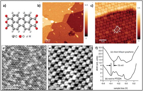
Initial work on molecular functionalization of graphene was focused on planar aromatic molecules such as PTCDA deposited via sublimation on epitaxial graphene grown on SiC (EG/SiC) )). The self-assembly of PTCDA molecules has been studied by different research groups on epitaxial graphene using scanning tunneling microscopy (STM) [Citation32–Citation34] in ultra-high vacuum (UHV) conditions at room temperature as well as at 77K. An important aspect of PTCDA SAMN formation on graphene is that the PTCDA domains don’t get discontinued at EG-SiC step edges but are in full compliance with graphene topology and propagate over step edges as shown in ). Slight n-type doping of graphene by PTCDA molecules was confirmed by Huang et al. [Citation33] and Lauffer et al. [Citation34] at low temperature in separate studies by scanning tunneling spectroscopy (STS) measurements ()). However, such n-type doping is not observed upon measurements at room temperature. Recently, H. J. Karmel et al. studied the structural and thermal stability of PTCDI molecules on a monolayer of G/SiC using UHV-STM and temperature-dependent X-ray reflectivity (XRR) [Citation35], showing a high thermal stability compared to PTCDA of up to 311.15 ± 10 K. Recent theoretical studies have suggested strong π-π interactions of these molecules with graphene, which potentially can result in doping as well as the introduction of a small bandgap.
Figure 1. (a) Molecular structure of PTCDA. (b) Large-scale STM image showing a monolayer SAMN of PTCDA on EG-SiC. (c) High-resolution STM image showing a continuous PTCDA layer over a step edge. Adapted with permission from ref. 32. Copyright © 2009 Nature Publishing Group (d) and (e) Molecular self-assembly of PTCDA on bilayer graphene. (f) STS spectra on pristine bilayer graphene compared with STS spectra on a region close to a PTCDA layer, showing a shift of 75 mV caused by charge transfer. Adapted with permission from ref. 34. Copyright © 2008 Wiley-VCH.
Due to different intermolecular interactions, TCNQ and its fluorinated counterpart F4-TCNQ self-assemble differently on graphene, as observed by Barja et al. and Stradi et al. in separate studies using high-resolution STM measurements [Citation36,Citation37]. With an electron affinity of 5.24eV the LUMO of F4-TCNQ is below the Dirac point of graphene, making it a very strong p-type dopant, as shown by Chen et al. for epitaxial graphene on SiC [Citation38]. Using high-resolution photoemission spectroscopy (PES) a clear evidence of electron transfer from molecules to graphene was obtained.
Metal phthalocyanines (MPc) are another class of molecules with an extended delocalized π-electron system, which have been used to functionalize graphene as well as other 2D materials. They are a class of highly stable molecules consisting of a macrocycle of alternating carbon and nitrogen atoms with a single metal atom in the center. Over the past few years, a number of MPc molecules with different central metal atoms have been studied on graphene grown on various substrates [Citation39–Citation42]. Thereby, MPc molecules have shown variable adsorption behavior on graphene depending on the level of coverage, peripheral functionalization and central metal atom as revealed by a number of separate STM studies. Mao et al [Citation39]. demonstrated the formation of a Kagome lattice of H2Pc, NiPc, and (t-bu)4-ZnPc molecules which follows the moiré pattern of underlying graphene. These Kagome lattices had different spins depending on the metal atom of the MPc molecule, which demonstrates the prospect of using these molecules to tune the spin interaction of graphene. A slight doping of graphene by a single layer of FePc molecules deposited in UHV conditions was revealed by Scardamaglia et al. using photoemission spectroscopy techniques [Citation43].
Additionally, organic molecules with long alkyl chains with functional groups are also used for controlled tuning of the doping levels of graphene. Li et al. showed that SAMNs of oleylamine (OA) molecules on graphene on SiC can result in n-type doping [Citation8] via electron transfer from the NH2 groups, while the alkyl chains direct the self-assembly of these molecules. Homogeneous SAMNs were observed by STM and AFM measurements in ambient conditions. The n-type doping caused by OA molecules was expected to modify the electronic properties of graphene and confirmed by electric transport measurements carried out on back-gated graphene field effect transistors (FETs), which showed a shift of the charge neutrality point towards more negative values (−16 V and −28 V) after the first and second deposition cycles of OA molecules.
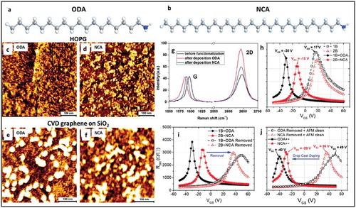
Recently, Phillipson et al. demonstrated the tuning of the Fermi level by varying the chain-length of alkylated amine molecules forming SAMNs on graphene [Citation44]. Control of the surface concentration of amino groups resulted in tunable n-type doping of graphene as shown by Raman spectroscopy measurements and charge transport characteristics measured by FETs (). Raman spectroscopy measurements carried out on octadecylamine (ODA) and nonacosylamine (NCA) functionalized graphene on SiO2 are shown in ). A higher n-type doping from ODA compared to NCA molecules was observed based on a larger redshift of the G peak position and a higher increase in the I(2D)/I(G) ratio. The charge carrier concentration found was 1.59 times higher with ODA compared to NCA, which is in good agreement with the ratio of alkyl chain length of NCA and ODA (1.6 times longer). The doping mechanism was explained by the formation of a dipole layer between graphene and the NH2 groups of ODA and NCA molecules. The transport measurements by FET also showed a 1.52 times higher doping for ODA functionalized devices compared to NCA functionalized ones.
Figure 2. (a) and (b) chemical structure of ODA and NCA molecules, respectively. (c) and (d) show AFM topographical images of ODA and NCA self-assembled on HOPG. (e) and (f) show AFM topographic images of ODA and NCA molecules self-assembled on CVD graphene. The lamellar structure of molecules is clearly observed in these images on both substrates. (g) Typical Raman spectra of CVD grown graphene before and after deposition of ODA and NCA. (h) Transfer characteristics of devices before and after functionalization with ODA and NCA via dip coating. (i) Transfer characteristics of devices doped and after dopant removal. (j) Transfer characteristics after doping by drop casting. Adapted with permission from ref 44. Copyright © 2016 The Royal Society of Chemistry.
Prado et al. showed p-type doping of graphene resulting from non-covalent functionalization via the formation of SAMNs using phosphonic acid molecules with long alkyl chains, namely octadecylphosphonic acid (OPA) and tetradecyl phosphonic acid (TPA), in ambient conditions [Citation45]. The phosphonic acid headgroup is an electron acceptor, leading to p-type doping of graphene. The molecules were deposited on graphene flakes exfoliated on SiO2 layers. AFM images showed well-organized monolayers consisting of OPA and TPA dimers, respectively. The alkyl chains of the molecules were arranged in a zigzag alignment aligned along a high-symmetry direction of graphene. Raman spectroscopy of the OPA functionalized graphene showed a shift of G peak (νG = 1586 cm−1) towards a higher wavenumber compared to the pristine graphene flake (νG = 1593 cm−1). A decrease in FWHM of the G-peak after functionalization and decrease in the I(2D)/I(G) ratio was also observed, which was attributed to p-type doping of graphene by the OPA molecules. However, no information was given concerning doping levels of graphene functionalized by TPA molecules.
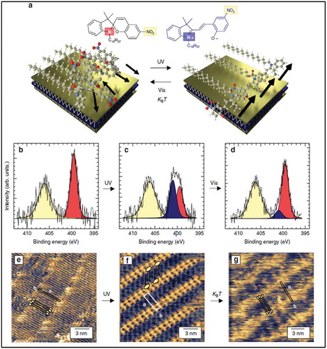
In all of the studies discussed above, tuning of graphene’s properties was achieved by varying the type of functional group and density of the molecules. Recently, P. Samorì and coworkers demonstrated the formation of periodic potential on graphene using SAMN formation. The surface potential of graphene was modulated by the change in dipole of the self-assembled molecules [Citation46]. Although this is an interesting aspect for the application of graphene for advanced electronics, it does not offer precise control, which future solid state devices based on graphene will require. One approach towards this goal is to include specific functional groups in self-assembling molecules, which can be modulated by external stimuli, also demonstrated by P. Samorì and coworkers [Citation47]. They showed that the transport properties of graphene and MoS2 can be modulated by using photochromic molecules. In this study, the authors have used a spiropyran (SP) derivative with an 18 carbon long alkyl chain for self-assembly on 2D materials. SP molecules can be reversibly switched to merocyanine (MC) forms, the latter having a large dipole moment. The conversion from the SP to the MC form takes place upon irradiation with ultraviolet (UV) light as shown by the schematic in ). The reversible reaction can be induced either thermally or by irradiation with visible light. Upon irradiation with UV-light, the change in the molecular dipole moments causes a shift in the work function of the 2D material. The isomerization from SP to MC upon UV irradiation was confirmed with STM in ambient conditions, as shown in . The SP isomer is characterized by a lamellar structure in which different rows of alkanes lie flat on the surface and are separated by bright fuzzy regions, while STM images after isomerization show fully immobilized MC groups lying close to each other and the alkyl chains form an interdigitated lamellar structure. Back-gated FET, fabricated using graphene, showed a strong shift in the charge neutrality point upon irradiating SP/graphene with UV light, suggesting a strong n-type doping with an electron density reaching = 4.4 × 1012 cm−2. This effect was reverted back upon irradiation with a green light. A similar effect was observed for SP/MoS2 hybrids. Irradiation at a precise location of the SP covered graphene leads to SP→MC isomerization only at that particular region, resulting in mixed transport characteristics of the devices.
Figure 3. (a) Schematic representation of SAMN monolayers formed by spiropyran derivatives on MoS2, undergoing photo-induced isomerization, leading to a structural rearrangement. Black arrows indicate the molecular dipoles, which align upon photo-induced isomerization. N1s core level spectra of SP molecules coated on HOPG when kept in the dark (b) after UV-irradiation (c) and after irradiation by green light (d), show different N hybridization states in agreement with the schematic in (a). High-resolution STM images of SP molecules on HOPG after spin coating (e) after UV irradiation (f) and) 48 h after UV-irradiation (g), showing molecular ordering upon UV irradiation. Adapted with permission from ref 47. Copyright © 2018 Nature Publishing Group.
Non-covalent functionalization of TMDs
Following different methods developed for the functionalization and tuning of the electronic properties of graphene by self-assembled molecules, similar approaches for other 2D materials such as TMDs and hBN were also developed. Bulk MoS2, one of the most studied material from the TMD family was used a number of times as an alternative substrate to study molecular self-assembly. Here we will discuss some of the studies which dealt with the modulation of properties of TMDs by molecules adsorbed on the surface. The pioneering work on the functionalization of MoS2 by SAMNs was carried out by M. Hara et. al, who used STM to determine the impact of substrates on the self-assembly of the smectic liquid crystal 4ʹ-n-octyl-4-cyanobiphenyl (8CB) at the air/solid interface [Citation48]. These authors have demonstrated that the molecules assemble in an energetically unfavorable manner due to strong interactions with the underlying substrate suggesting epitaxial growth of molecular layers on the MoS2 lattice. A year later Cincotti et al. demonstrated SAMN formation of dotriacontane (C32H66) molecules at the liquid-MoS2 (and MoSe2) interface [Citation49]. These initial studies were mostly focused on using TMD as substrates for a better understanding of molecular self-assembly forming SAMNs and the impact of the lattice structure of the underlying surface.
An interesting approach towards tuning the physical and chemical properties of TMD is using self-assembled monolayers (SAMs) [Citation50,Citation51]. In contrast to SAMNs, where the molecules are physisorbed on the surface, typically with their long axis parallel to the surface, SAMs are formed by molecules consisting of (i) a functional anchoring group such as thiol, silane or phosphoric acid to chemisorb molecules on the target substrate, (ii) a molecular backbone, typically alkyl chains, which can stabilize the SAM via intermolecular van der Waals interactions and (iii) a functional head group, which determines the surface energy and dipole moment after SAM formation, thereby allowing to tune the physicochemical properties of the exposed surface. The interactions among the molecular backbone of the SAMs generally result in high crystallinity, which causes molecules to orient edge on with respect to the substrate plane. This makes it possible for single molecule dipoles to sum up and align, resulting in a sufficient electric field to interact with TMDs. In addition to acting as a substrate for the deposition of a SAM [Citation49,Citation52], TMDs can also be deposited on SAM-modified substrates[Citation53]. When TMDs are in contact with a SAM, the dipole moments of the end functional groups affect the Fermi levels of TMDs. An upward or downward shift of the TMD Fermi level may occur depending on the functional group, resulting in doping of TMDs.
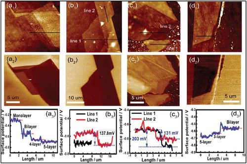
Molecular doping of TMDs, such as MoS2 and WSe2, by self-assembled monolayers (SAM) with a silane anchoring group has been demonstrated to result in the tuning of the optoelectronic properties in a number of experimental studies [Citation53–Citation57]. Li et al. studied the doping behavior of different molecules with a silane end group, such as octyltrichlorosilane (C8H17SiCl3)(or OTS); 3-(trimethoxysilyl)-1-propanamine (NH2(CH2)3Si(OCH3)3)(or APTMS); and trichloro(1H,1H,2H,2H perfluorooctyl)silane (CF3(CF2)5CH2CH2SiCl3) (or FOTS), with different dipole moments to modify the work function of MoS2 [Citation53]. These molecules form monolayers on SiO2 and therefore can act as an interface between MoS2 and SiO2. The self-assembled monolayers of these molecules were characterized using AFM and XPS. KPFM, Raman Spectroscopy and transport characteristics by FET were used to determine the modulation in the doping levels of MoS2. Depending on the dipole moment and polarity, these molecules showed different hole and electron doping abilities. MoS2 on OTS SAMs showed very little change in Raman spectra compared to pristine MoS2 flakes with the same thickness on SiO2, suggesting very little charge transfer between MoS2 and the octyltrichlorosilane (OTS) molecules. However, for substrates functionalized by APTMS and FOTS, blue shifts of 1.6 cm−1 and 1.7 cm−1, respectively, were observed. Spatial charge distribution measurements to determine the charge transfer between MoS2 nanoflakes and SAM-modified SiO2 surface were carried out using KPFM, showing a shift of the Fermi levels of monolayer MoS2 by more than 0.45 eV due to the interactions with FOTS and APTMS, respectively. shows a clear contact potential difference (CPD) between different layers of MoS2 flakes deposited on the SAM-modified SiO2 surface. A shift in the Fermi level, calculated from CPD measurements, confirms the charge transfer process between the molecules and MoS2.
Figure 4. (a1-d1) AFM topographic images of MoS2 flakes and (a2-d2) KPFM surface potential maps corresponding to the areas sown in a1-d1. (a3-d3) show the corresponding surface profiles. Adapted with permission from ref 53. Copyright © 2013 American Chemical Society.
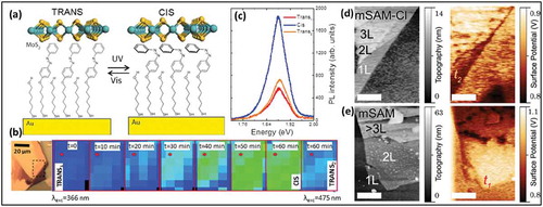
These studies showed the possibility to induce unique characteristics in TMDs by using molecules of interest as SAMs, as recently demonstrated with SAMs composed of thiolated photochromic azobenzene (AZO) molecules (E)-6-(4-(phenyldiazenyl) phenoxy)hexane-1-thiol (HS-C6AZO) and (E)-6-(4-((4-chlorophenyl) diazenyl)phenoxy)hexane-1-thiol (HS-C6AZO-Cl) as electropositive and electronegative SAMs chemically attached to a gold substrate [Citation58] as shown in )). These molecules were mixed with spacer molecules (6-(2-mercapto)-1-hexanol) to form mixed monolayers. Azo molecules are photochromic and can be switched between a cis and a trans isomer upon irradiation of light at a different wavelengths. In this work, photoswitching of molecules between the cis and trans state resulted in a modification of surface energetics of single MoS2 layers deposited on top of the SAMs. The change in the surface potential of MoS2, resulting from photoswitching between cis and trans state, was demonstrated using KPFM. Photoluminescence (PL) measurements revealed that for n-type phototunable doping the PL intensity between trans-mSAM and cis-mSAM is increased ()), while the opposite behavior was recorded for phototunable p-type doping. This Au/AZO-SAM/MoS2 stack was also used to demonstrate the application in photo switchable vertical diodes. In these diodes, the current flowing vertically through the Au/SAM/MoS2 stack is measured by placing a conductive AFM tip in contact with MoS2. Current rectification behavior was observed when the AZO-SAM is in the trans state, which is suppressed when the AZO-SAM is isomerized to cis state, thus demonstrating the possibility to reversibly tune the energetics of TMDs using molecular capabilities such as photoswitching.
Figure 5. (a) Schematic of a diazo gated sample in trans and in the cis state. (b) Series of the PL intensity recorded from the MoS2-mSAM after UV exposure, irradiating the sample for the different duration and switching back to trans state after 120 min of white light exposure. (c) PL spectra showing switching from trans to cis and back to trans states (d) AFM (left) and KPFM (right) measurements recorded from multilayer MoS2-mSAM-Cl and (e) from multilayers MoS2-mSAM samples in trans state. Adapted with permission from ref 58. Copyright © 2014 American Institute of Physics.
An n-type doping of MoS2 nanoflakes on SiO2/Si using SAMNs of physisorbed oleylamine (OA) molecules was recently reported as an efficient way to reduce the contact resistance between metal contacts and MoS2 in FETs [Citation59]. AFM measurements revealed that OA molecules were self-assembled on the MoS2 surface in the form of lamellar domains as shown in ). Raman and PL spectroscopy along with electrical characterization using a four probe back-gated FETs showed clear evidence of n-type doping of MoS2 resulting from OA molecules shown in ). An increase in ION by a factor of 1.9 suggested an increase in the carrier concentration arising from doping by amine groups. The increased carrier concentration was also attributed to the negative dipole moment of the amine groups that influence the tunneling of interface-trapped carriers to the conduction band of the MoS2 film.
Figure 6. AFM images of an oleylamine functionalized MoS2 flake (and d) and the corresponding height profile (b). (c) shows Raman spectra before and after functionalization of the MoS2 by oleylamine molecules. A tentative model of self-assembled oleylamine molecules is shown in (e). Transport characteristics before doping, after doping and after removal of OA doping are compared in f. Adapted with permission from ref 59. Copyright ©2016 American Institute of Physics.
Benzyl viologen (BV) is one of the most used molecules to understand and study the impact of doping on properties of MoS2. Kiriya et al. have studied confocal absorption spectra for doped and undoped MoS2 samples [Citation60]. In this study, the authors used BV to induce n-type doping in MoS2. Air-stable benzyl viologen was adsorbed on the surface of few-layer MoS2, which resulted in a stable charge transfer doping. The charge transfer doping between BV molecules and MoS2 was probed by using the functionalized MoS2 in FET devices in back gate configuration and by Raman spectroscopy of the functionalized MoS2. After doping with BV molecules, the MoS2 FET devices did not show gate voltage dependence of the on current (IDS), which was increased by an order of magnitude (IDS = 1.3 × 10 − 4 A at VGS = 40 V). Poor gate voltage dependence and the increased current density are clear indications that MoS2 was strongly doped by BV molecules. Devices of doped MoS2 retained the observed characteristics with minimal changes even after 9 days of exposure to ambient conditions. Reversing the functionalization of MoS2 by immersing the devices in toluene lead to increasing the gate voltage dependence of the current, similar to the curve obtained for pristine MoS2 FETs. This shows that BV molecules on MoS2 form air stable charge transfer complexes, which disintegrate upon immersing the MoS2 layers in toluene. Raman spectroscopy carried out on BV functionalized MoS2 showed a shift in the A1g vibration modes towards lower wavenumbers compared to non-functionalized MoS2 as a result of high electron concentration. These studies suggest that physisorbed molecules can potentially be used for air-stable and reversible functionalization of few-layer MoS2.
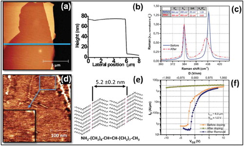
For tuning the properties of MoS2, several molecules which have been thoroughly studied on graphene were also used. F4-TCNQ was used as a p-type dopant of MoS2 in a couple of studies [Citation61,Citation62]. Wang et al. [Citation62] recently reported that charge transfer from MoS2 to F4-TCNQ leads to the formation of van der Waals interface when the molecules are deposited on MoS2 surface in vacuum conditions ()). The molecules lead to p-doping of the MoS2 layer along with a depletion of residual electrons from the sulfur vacancies, resulting in bringing the onset voltage value of the MoS2 FET close to zero, while no reduction in the mobility of MoS2 FETs were observed after the deposition of F4-TCNQ molecules. Scanning Kelvin probe force microscopy studies further verified the charge transfer mechanism ()). The authors have also shown that such interesting charge transfer effects in van der Waals interfaces between organic-inorganic hybrid systems can have potential applications for sensing applications, as illustrated by using this hybrid system in FET configuration for NH3 sensing. F4-TCNQ was also deposited on MoS2 flakes by solution-based techniques. Mouri et al. [Citation61]. studied doping characteristics of molecules including F4-TCNQ drop casted on MoS2 flakes. They have shown that depositing F4-TCNQ molecules on MoS2 leads to a strong enhancement in PL intensity of the MoS2. This enhancement was the result of switching the dominant PL process, i.e. the recombination of the negative trion which usually occurs in as-prepared 1L-MoS2, to the recombination of the exciton instead.
Figure 7. (a) Surface topography of F4-TCNQ functionalized MoS2, showing island-like F4-TCNQ particles with an average height around 20 nm. (b) Surface potential distribution of the same area as in a), the dark areas correspond to F4-TCNQ island sites. (c) and (d) show surface topography and potential distribution, respectively, after annealing the samples, (e) shows cross-section profile of the lines marked in (c) and (d). (f) Schematic of space charge region in F4-TCNQ molecules. Adapted with permission from ref 62. Copyright © 2018 Wiley-VCH.
Functionalization of MoS2 based photodetectors by organic dyes, such as perylenediimides (PDIs) and porphyrins (TPP), resulted in an increase of photocurrent and responsivity up to 3 times higher compared to pristine MoS2 based photodetectors [Citation63]. AFM measurements confirms the formation of 5–36 nm thick layer of TPP molecules on MoS2 flakes. In another work, perylene-based molecules were used as a seeding layer for atomic layer deposition of Al2O3 gate dielectric.
Non-covalent functionalization of hBN and black phosphorus
Its large electronic bandgap (~5.2 eV) makes hBN a good decoupling layer to study the electronic properties of individual or self-assembled molecules without much influence from the underlying substrate. Molecular functionalization is an effective method to tune the electronic, magnetic or metallic properties of hBN. However, here the presence of the large bandgap is a major drawback of hBN. Willi Auwärter discussed the self-assembly of most of the molecular systems on hBN in a comprehensive review [Citation64].
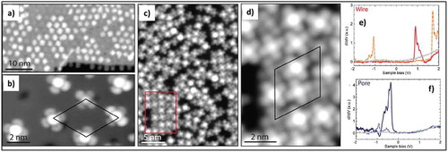
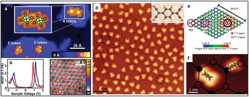
In the case of hBN epitaxially grown on metallic substrates such as Ni(111), Rh(111) and Ru(0001), strong interactions and a lattice mismatch of the hBN with the underlying substrate result in the formation of a nanomesh. This nanomesh can be used for preferential deposition of single molecules at low coverage and hence allows the study of electronic properties of molecules without any external influence, as reported by Schulz et al. [Citation65]. It was shown by STM and STS that CoPc molecules adsorb preferentially in the nanomesh at low coverage, but at high coverage form larger square-shaped islands. STS measurements on the metal central atom of CoPc gave different spectra for molecules adsorbed in the pore and on wire regions of the nanomesh. STM measurements at different biases resulted in different contrasts from the metal center and carbon backbone depending on the applied bias. Based on STS spectra it was concluded that the LUMO of the molecules in the pores are below the Fermi energy compared to a molecule on the wire, suggesting an ordered charging of the molecule in pores as shown in ).
Figure 8. (a) and (b) STM images of CoPc self-assembly in the low coverage regime with one molecule per moiré unit cell. (c) and (d) Higher coverage results in filling the wires with locally square-packed regions. The image in panel d corresponds to the area marked by the red rectangle in panel c. (e) STS Spectra measured on CoPC adsorbed in the wire region of the moiré unit cell; red solid line is measured on the metal center and orange-dashed line on the carbon backbone. (f) STS spectra measured on a molecule adsorbed in the pore region of the moiré unit cell; the dark blue solid line is the metal center and dashed light blue the carbon backbone. Adapted with permission from ref 65. Copyright © 2013 American Chemical Society.
The wide bandgap makes it difficult to study the impact of functionalization on hBN properties. However, photoluminescence and Raman spectroscopy were used to study the vacancy defects in the hBN lattice. Nitrogen or boron vacancies in the hBN lattice can create additional states in the electronic bandgap of hBN, which leads to interesting PL behavior. Molecular doping of hBN is another approach towards tuning the electronic bandgap of hBN, which can be studied using PL and Raman spectroscopy.
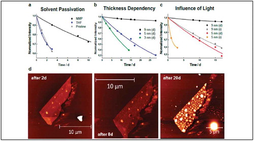
Functionalization by wet-chemical treatment of liquid phase exfoliated black phosphorus (BP) has been shown to be successful with electron-poor TCNQ as well as a perylene diimide (PDI) derivative by the group of A. Hirsch [Citation66]. In the case of TCNQ, an electron transfer from BP to the dopant took place, while the interactions between BP and PDI were mainly based on van der Waals forces. These strong interactions between the organic molecules and BP supported the liquid phase exfoliation of bulk BP into a few layer BP flakes. Additionally, the functionalization with PDI increased the resistance of the BP flakes against oxygen degradation. Since the lack of stability and degradation of BP in ambient conditions is a major drawback of this material in few of potential applications, the latter finding prompted a systematic study on the oxidation and passivation behavior of mechanically exfoliated BP by the same group [Citation67]. The oxidation of BP was monitored by statistical Raman spectroscopy and various factors affecting the stability of BP flakes were investigated, i.e. layer thickness, lateral dimensions, and exposure to light. Basically, the stability of few-layer BP flakes increased with thickness and light illumination led to a faster degradation ()). In this study it was also found that treatment with ionic liquids like N-methyl-2-pyrrolidone (NMP), significantly increased the stability of BP by several days ()).
Figure 9. (a) Effect of NMP passivation compared to an inert solvent (THF) and a pristine sample on ca. five nm thick flakes with the comparable area. (b) Influence of thickness on the degradation of NMP-protected flakes stored in darkness, clearly surpassing 25 days of stability. (c) Influence of continuous visible light illumination on 5 and 9 nm thick flakes. (d) AFM images showing a 9 nm flake protected with NMP after 2, 8, and 20 days under ambient conditions. Adapted with permission from ref 67. Copyright © 2017 American Chemical Society.
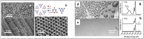
In the context of stabilizing BP under ambient conditions, Korolkov et al. successfully formed SAMNs stabilized by hydrogen bonds by solution deposition to passivate BP and inhibit oxidation under ambient conditions [Citation68]. The molecules used were trimesic acid (TA) and melamine cyanurate (CA.M), which are known to form supramolecular networks on other 2D materials. AFM images with molecular resolution in ambient conditions showing molecular self-assembly could be obtained ()), indicating an atomically flat surface of BP. Comparison of optical micrographs and XPS spectra of passivated and non-passivated BP after several days up to three months showed a clear passivation effect of the molecular layers ()). Even after 1 month in ambient conditions, atomically resolved AFM images of the BP could be obtained.
Figure 10. High-resolution AFM images of CA.M deposited on BP (a). Arrows indicate the direction of the principal axis of the CA.M structure, which is aligned with the BP rows. The inset shows the underlying BP.(b) A schematic of melamine, cyanuric acid and the CA.M complex (c) A high-resolution AFM image with individually resolved molecules. (d-e) Optical micrographs and (g-h)XPS spectra taken illustrating the passivation of BP by CA.M by comparing non-passivated BP exposed to ambient conditions (d and g) BP passivated with CA.M (e and h). Adapted with Permission from ref 68. Copyright © 2017 Nature Publishing Group.
In addition to studies concerning the stability of BP, non-covalently modified BP has also been used in FETs. Han et al. showed that surface functionalization of few-layer BP with potassium (K) can increase the performance of FET [Citation69]. Therefore, mechanically exfoliated BP was used for FET fabrication and K was evaporated onto the devices under UHV conditions. Compared to the non-functionalized devices, the electron doping effect of K resulted in significantly improved electron mobility by over one order of magnitude and a clear bandgap reduction. Complementary in-situ UPS and XPS measurements were carried out with K-modified bulk BP and confirmed the interfacial charge transfer taking place at the K/BP interface leading to the electron doping effect.
Covalent functionalization of 2D materials
The functionalization methods discussed so far to tune the properties of 2D materials involved the physisorption of molecules on the basal plane. This approach, however, suffers from drawbacks in terms of robustness of the process and stability of the molecule-2D material interactions. Due to the weak interactions between physisorbed molecules and the 2D material, external stimuli can easily alter the properties of these systems. In this regard, covalent attachment (or grafting) of molecules on 2D materials provides a more robust approach for controllably tuning the properties of 2D materials. Similar to graphene, TMDs, hBN and black phosphorus have also been covalently modified using diazonium chemistry and other chemical approaches. In this section, we will be discussing the most prominent functionalization strategies for covalent functionalization of these 2D materials.
Covalent functionalization of graphene
Covalent functionalization results in rehybridization of sp2 carbons to sp3 carbons by forming bonds with reactive molecules on the basal plane of the graphene lattice. This process is similar to creating defects in the graphene lattice and therefore leads to a modification of the electronic band structure, magnetic, optical and mechanical properties of graphene. Additionally, covalent functionalization can lead to better solubility and processibility of graphene, which is an important aspect for more practical applications. Till today, a number of functionalization methods such as addition of diazonium radicals [Citation10,Citation12,Citation70–Citation76], Diels-alder reactions [Citation77–Citation80], cycloaddition reactions [Citation13,Citation81,Citation82], nitrine addition [Citation83,Citation84] and carbene addition [Citation85] have been developed for the covalent grafting of molecules on graphene basal plane. Among these methods, covalent functionalization of graphene using diazonium chemistry is the most efficient and versatile. Diazonium chemistry can also be extended to other 2D materials as evident from the recent studies discussed later in this section. First, we will discuss different methods for covalent functionalization of graphene and other 2D materials.
Functionalization of graphene by diazonium chemistry proceeds via a radical mechanism, where the diazonium salt is reduced to form an aryl radical, which subsequently reacts with the surface as shown in ). Haddon and coworkers were the first to demonstrate covalent functionalization of graphene using diazonium chemistry [Citation70,Citation86]. They showed the functionalization of epitaxial graphene on SiC by spontaneous grafting of aryl groups via reduction of 4-nitrobenzenediazonium (NBD). FTIR-spectroscopy and XPS measurements confirmed the presence of nitro groups on the functionalized graphene. The surface coverage was estimated to be 1 × 10¹⁵ molecules/cm2 based on cyclic voltammetry measurements. Additional work from Haddon and coworkers used spectroscopy methods to study the impact of covalent grafting on the electronic properties of graphene. Using a combination of Raman spectroscopy with ARPES, the authors demonstrated how the covalent functionalization with NBD affects the electronic properties of graphene. Raman measurements carried out on flakes as well as on epitaxial graphene on
Figure 11. (a) Schematic showing the spontaneous reduction of p-nitrobenzene diazonium (NBD) and its reaction with graphene, leading to covalent attachment of aryl groups to graphene Adapted with permission from ref 86 Copyright © 2011 American Chemical Society. (b) ARPES measurements of NBD-functionalized graphene showing the band structure perpendicular to the Γ-K direction at the graphene K-point (incident photon energy is 36 eV). Two diffuse bands representing gapped Dirac cones are visible. (c) Changes in the Raman spectra in exfoliated and epitaxial graphene due to NBD-functionalization, ID/IG = 3.3. d and (e) Comparison of AFM images of pristine EG and NBD-EG, respectively. Adapted with permission from ref 10. Copyright © 2010 American Chemical Society.
SiC showed a pronounced D peak of functionalized graphene ()). The D peak is associated with defects in the basal plane of graphene, which in this case was caused by the grafted NBD molecules. ARPES measurements showed a slight transformation of linear dispersion of graphene into massive particle dispersion with the Dirac point shifting to 0.36 eV below the Fermi level as shown in ).
Further, SPM-based techniques have been used to determine and control the locations of the molecules covalently bound to graphene. Hossain et al. used UHV-STM to study the morphology of graphene with covalently functionalized 4-NBD molecules [Citation87]. STM images revealed that certain areas of the 4-NBD functionalized graphene did not show any sign of grafting, which was attributed to a blocking effect of oligomers formed during the grafting reaction as shown in ). The aryl oligomers possibly form as a side product of the reaction between nitrophenyl radicals in solution with already grafted molecules. STS spectra revealed no clear modification of graphene’s intrinsic properties in blocked areas, whereas STS on functionalized areas showed a high perturbation of electronic band structure of graphene as shown in ). Later on, Greenwoood et al. used STM and Raman spectroscopy to study the grafting of different diazonium salts on graphene and HOPG [Citation12]. A comparison between grafting morphology and molecular structure for 4-NBD and bulky 3,5-bis-tert-butylbenzenediazonium (3,5-TBD) was done ()). It was demonstrated that the density of the grafted molecules on graphene and HOPG can be controlled by using diazonium molecules with appropriate substituents, i.e. bulky substituents help in creating a monolayer of grafted molecules with high density. STM tip-induced lithography showed the potential of this technique to remove the grafted molecules from the substrate and restore the pristine graphene or graphite surface, respectively.
Figure 12. (a) STM image of the chemically modified graphene surface preceding nanopatterning. (b) STM image following bias-dependent nanopatterning of three horizontal lines at a constant tunneling current (1.0 nA) and tip velocity (100 Å/s). (c) Additional nanopatterning of three vertical lines, showing linewidths at the sub-5 nm length scale. All STM images were acquired at a sample bias of +1.85 V and tunneling current of 0.06 nA. Adapted with permission from ref 87. Copyright ©2010 American Chemical Society. STM images of clusters after grafting from a 1 mM solution of (f) 4-NBD and (g) 3,5-TBD on CVD graphene on Cu, (h) The Raman spectra showing strong D peak at 1332 cm−1, confirms grafting of diazonium molecules. Adapted with permission from ref 12. Copyright © 2015 American Chemical Society.
Detailed studies on the electron transfer between grafted molecules and graphene were summarized by Strano and coworkers in comprehensive reviews [Citation74,Citation88]. Wang et al. showed the influence of the substrate underneath graphene on the reactivity of graphene, which can be exploited to control the diazonium chemistry [Citation75]. Localized grafting can be achieved by patterning the substrate supporting graphene. Raman maps of the D/G ratio and AFM measurements confirmed patterned grafting.
Another approach for patterned grafting of diazonium molecules on graphene was demonstrated by Xia et al. by using long alkyl chains attached to diazonium molecules [Citation89]. CVD graphene was functionalized by 4-docosyloxy-benzenediazonium tetrafluoroborate (DBT) molecules. The long alkyl chains promoted self-assembly of DBT molecules, leading to the formation of a SAMN on graphene ()). The diazonium molecules were then activated electrochemically, resulting in patterned grafting. STM, AFM, Raman spectroscopy and conductivity measurements showed significant modifications in the properties of graphene, thus confirming covalent functionalization.
Figure 13. (a) STM image of DBT molecules assembled on HOPG, the schematic on the image shows possible molecular packing. STM height (b) and current (c) images of DBT molecules assembled on graphene show a similar contrast. d) Raman spectra of graphene/SiO2 substrate after spin coating of DBT (0.5 mM in CHCl3), electrochemical grafting, and washing. Adapted with permission from 89 Copyright © 2016 American Chemical Society. e) An illustration for an EC cell contains a solution double layer consisting of an aqueous phase containing diazonium molecules (light blue) and an organic templating phase(red). f) A schematic representation for linear grafting through the self-assembled molecular network of alkane template (g-j) STM images of functionalized samples showing a linear pattern of the grafted molecules, obtained by using pentacontane (g), tetracontane (h), and triacontane (i) in tetradecane as templates. Adapted with permission from 90. Copyright © 2018 American Chemical Society.
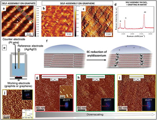
An interesting method for patterning grafted molecules on graphene is using self-assembled molecular monolayers, as recently demonstrated by Tahara et al [Citation90]. In this method, graphene/graphite was covalently functionalized by few nanometer wide rows of 3,5-TBD molecules using SAMNs of long-chain alkanes as a template. This approach relies on phase separated solution double layer as shown in ). A first solution layer contains n-alkane molecules which self-assemble on the surface of graphene/graphite. A second solution layer contains diazonium molecules which diffuse through the first layer upon a potential sweep in the electrochemical cell and get reduced to diazonium radicals. These diazonium radicals attack the available graphene/graphite area and form organized covalent bonds with the surface. Using n-alkane networks of different sizes the periodicity of covalently grafted molecules can be controlled. The organic layer plays a critical role in this method by allowing lateral displacement of n-alkane terminal edge around which the alkyl radical attack occurs. Raman spectroscopy and STM confirmed covalent grafting of molecules on HOPG and graphene. STM images clearly showed the patterned grafting of 3,5-TBD molecules as shown in )
Diels-Alder (DA) cycloaddition reactions on graphene were thoroughly studied by Haddon and coworkers [Citation77,Citation79]. Due to the absence of an electronic bandgap, graphene can act as either diene or dienophile for DA reactions. Using STM, Raman spectroscopy and ARPES, the authors have demonstrated the covalent grafting of different molecules such as tetracyanoethylene (TCNE) and maleic anhydride (MA), where graphene acts as diene and with 2,3-dimethoxy-1,3-butadiene (DMBD), where graphene acts as a dienophile. Due to the formation of two sp3 bonds between the molecules and graphene, this approach is highly promising towards selective functionalization of graphene with the potential for atomically precise patterning for CMOS technology. L. Simon and coworkers [Citation13] showed the modification of the Fermi velocity of electrons upon increasing the grafting density of fluorinated maleimide molecules using ARPES. The authors have proposed a method for determining the location of grafted molecules by systematically analyzing the pattern of standing waves generated by quasiparticle scattering of electrons.
Apart from diazonium grafting there are several other approaches towards covalent functionalization of graphene. One such approach was shown by Bueno et al. by functionalizing graphene by p-aminophenol (p-AP), which can covalently bind to graphene on the site of dangling bonds surrounding vacancies in the graphene lattice [Citation91]. UHV-STM images and XPS confirmed the covalent attachment of p-AP molecules on graphene and the impact of grafting on the electronic band structure of graphene was evident by ARPES studies (). Cycloaddition reactions of graphene with aromatic molecules can also result from interactions of graphene with the underlying substrate. For graphene on Ir(111), weak covalent interactions between C atoms and Ir atoms arise in the areas of the moiré pattern where C atoms are located on top of Ir atoms due to π-d hybridization. As a result, there can be unsaturated dangling bonds that are located on C atoms in hollow sites of the Ir lattice. Altenburg et al. showed that different MPc molecules at lower coverage adsorb distinctly by binding to the graphene layer with one to three Pc lobes [Citation92]. It was reported that most of the MPc molecules are physisorbed and form dimers or clusters, but some of the MPc molecules show only two or less lobes and are immobile as observed by STM images as shown in ). STS spectra of the four lobes state compared with the three lobes state showed a shift of peaks by 200–300 meV for the three-lobed states, which was further downshifted for two-lobed or one lobed state ()). DFT calculations confirmed a cycloaddition reaction taking place between MPc molecules and C atoms of graphene. It was concluded that the molecules react on the fcc sites of graphene.
Figure 14. (a) Atomic-resolved STM image of the (6√36√3)R30 reconstruction of the SLG epitaxially grown on SiC(0001) (b) STM image of single atom vacancies formed upon argon irradiation on the surface (c) STM image obtained after dosing the vacancies with 4L of p-AP; (d)Top and side views of the optimized model for a single-vacancy created within a SLG on a graphene buffer layer and top and side views of the optimized geometry of a doubly dehydrogenated p-AP molecule with the nitrogen atom integrated within a monovacancy in the SLG lattice (e) N 1s core level spectra after p-AP grafting on a SLG surface without and with atomic vacancies. (f) ARPES spectra of a p-AP functionalized SLG. Cut along kx direction. Adapted with permission from ref 91. Copyright © 2017 Nature Publishing group.
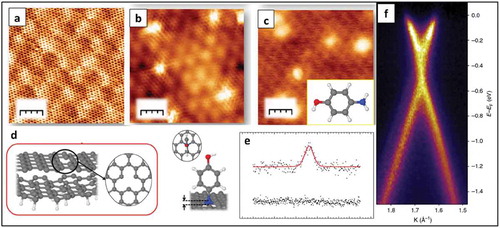
Figure 15. (a) STM image of FePc on graphene islands on Ir(111) showing FePC molecules in different-lobed states. Inset: Zoom-on four-lobe FePc dimer overlaid with the molecular structure. (b) dI/dV spectra obtained at the center of the four-lobe (blue) and three-lobe (red) species. (c) Large-scale STM image of three-lobe FePc molecules on graphene on Ir(111) with superimposed red lines showing the moiré lattice. The positions of the missing lobes of the molecules are indicated by white dots. Adapted with Permission from ref 92. Copyright © 2015 American Chemical Society (d) STM image of F4TCNQ molecules adsorbed on G/Ir(111) surface. Most of the molecules are in the two-legged configuration; one molecule in flat geometry is highlighted by a black circle. The moiré unit cell is indicated by the black parallelogram. The black dots indicate the corners (fcc sites) of the moiré pattern. (e) Illustration of the G/Ir(111) moiré unit cell depicting different registries between the carbon atoms and the underlying Ir substrate. (f) STM topography image showing the two-legged and flat adsorption geometries with respect to the G/Ir(111) moiré. The fcc and hcp regions have been depicted by filled and open circles. Adapted with permission from ref 93. Copyright © 2017 American Chemical Society.
Similar studies carried out by Kumar et al. showed the covalent bond formation between graphene and a cyano group of F4-TCNQ molecules [Citation93] by STM/STS and nc-AFM. The molecules showed varying adsorption geometry on different sites of a moiré unit cell of graphene on Ir(111), which resulted in a change of the molecular electronic structure. On fcc sites of the G/Ir(111) moiré, the molecules shows a two-legged structure, whereas on hcp and top sites the molecules were lying flat on the surface ()). Further, the molecular configuration could be manipulated by the STM tip. STS measurements revealed that in two-legged geometry the molecules were charged, whereas in the other geometry the molecules remained uncharged. Two possible reasons were identified for the observed charging: a) a tradeoff between tilt-induced charging and reduced van der Waals interactions and b) partial rehybridization of graphene carbon atoms into sp3 configuration with enhanced bonding interactions with the cyano groups of F4-TCNQ molecules.
The impact of functionalization by aryl diazonium molecules on electronic transport properties of graphene has been explored in a number of different studies [Citation73,Citation94,Citation95]. A. Jacobsen et al. showed that diazonium chemistry has an effect on the transport characteristics of graphene. Transport measurements of conductance (G) as a function of backgate voltage (VBG) at room temperature showed that after functionalization by NBD, a p-type doping is induced in graphene. A shift in the Dirac point from +9V to +31V were observed with increasing functionalization. H. Zhang et al. performed transport measurements on mechanically exfoliated graphene flakes before and after functionalization with 4-NBD molecules [Citation95]. I-V, as well as conductance measurements for pristine graphene devices, did not show much dependence on temperature characteristics. However, after functionalization the I-V characteristics of the devices showed a linear to non-linear transition upon decreasing temperature from 300 K to 4.2 K. This transport behavior of graphene was in agreement with the variable range hopping (VRH) model, suggesting that diazonium functionalized graphene behaves as granular metal with a bandgap of ~100 mV at low temperatures.
Covalent functionalization of TMDs
Several studies have been published in the past few years on covalent functionalization of TMDs by different methods. Most of the studies were focused on covalent functionalization of TMD nanosheets obtained by solution processing via ion intercalation [Citation23,Citation26] or by ultrasonication [Citation18,Citation96]. Following the successful demonstration of TMD nanosheets functionalized with alkyl halides and diazonium chemistry in solution, this approach was also applied for the functionalization of TMD nanosheets supported on different substrates. We have focused mostly on the functionalization of TMDs by diazonium chemistry, reaction of alkyl halides and thiol chemistry.
The pioneering work on covalent functionalization of transition metals in cluster form was reported by Tuxen et al [Citation25]. In this work, the authors have shown the impact of MoS2 cluster size on the adsorption efficiency of dibenzothiophene (DBT) and methyl substituted DBT (4,6-DMDBT) molecules with high-resolution STM images. MoS2 clusters of different sizes react differently with the DBT molecules, depending on the cluster edge preference for S vacancy formation.
In 2015, Chhowala and coworkers showed a general route towards covalent functionalization of TMDs by attaching organohalide and aryl diazonium molecules to the basal plane of 2D TMD nanosheets [Citation29]. In this work, the TMD nanosheets were first converted into a metallic 1T/1T’ polytype using n-butyllithium, followed by functionalization with 2-iodoacetamide and iodomethane. This approach also allows the functionalization of substrate-supported CVD MoS2 nanosheets and functionalization with 4-bromobenzene diazonium molecules. The electron rich 1T/1T’ polytype transfers charge to the organohalide (or diazonium) molecules resulting in around 30% of functionalization as confirmed by XPS studies. Structural characterization by atomically resolved transmission electron microscopy (TEM) measurements suggested that the octahedral coordination of the TMD nanosheets is not affected by the functionalization. Afterwards, studies by Knirsch et al. with a similar approach in liquid phase showed that pre-existing defects are not required for the functionalization of TMDs [Citation26]. To produce MoS2 nanoflakes without pre-existing defects, chemical exfoliation (CE) by intercalation of n-BuLi was performed in presence of an excess of MoS2 powder, resulting in an almost 1:1 ratio for 2H and 1T polymorphs as shown by XPS results. Chemically exfoliated MoS2 has been functionalized with 4-methoxyphenyldiazonium tetrafluoroborate. The covalent functionalization was confirmed by XPS, IR spectroscopy and TGA in combination with mass spectroscopy. After covalent functionalization, the 1T polytype of MoS2 showed semiconducting behavior. This approach can be used for attaching various organic functionalities on TMDs using diazonium or alkyl halide interface [Citation97,Citation98]. However, while for most of the proposed applications of TMDs it is desirable to study the impact of covalent functionalization on substrate-supported TMDs, functionalization of substrate-supported TMDs was not carried out.
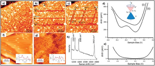
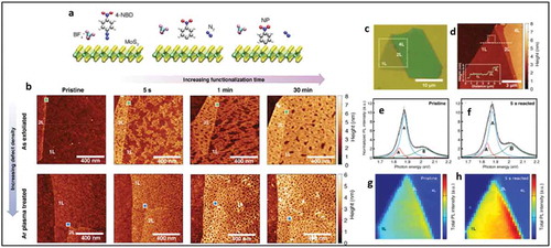
Recent studies by Chu et al. have addressed the issue of covalent functionalization on the basal plane of substrate-supported TMDs [Citation27]. The authors have shown by SPM, XPS, Raman and PL spectroscopy, TGA analysis and scanning electron microscopy (SEM) that 4-nitrobenzene diazonium molecules can be grafted on the surface of mechanically exfoliated as well as CVD grown MoS2 layers. Exfoliated MoS2 flakes on Si/SiO2 were subjected to an aqueous solution of 4-NBD molecules. A change in surface topography of MoS2 flakes was observed by AFM measurements on single layer regions of MoS2 as shown in ). Theoretical calculations predicted a higher probability of grafting of molecules near the defect sites or close to the already grafted molecules as a result of a higher surface dipole moment in proximity to these sites which is evident by complete coverage of NBD molecules on Ar plasma treated MoS2 after very short reaction times (5s). A high PL yield was observed for NBD functionalized monolayer MoS2 when compared to few-layer MoS2 due to a direct bandgap in monolayer MoS2 ()). An increase in C-S peak intensity as a function of increasing functionalization duration on CVD MoS2 was observed in the C1s XPS spectra, confirming the covalent nature of the bond between 4-NBD molecules and MoS2. Further, the authors have shown that diazonium chemistry can be used for biosensing applications. Therefore, 4-carboxylbenzene diazonium molecules were first grafted on MoS2 samples and subsequently reacted with polyhistidine (His)-tagged green fluorescent protein (GFP) and the red fluorescent protein, mCherry. The surface was probed using confocal fluorescence microscopy, which showing bright field optical images along with fluorescence images in the green and red channels for GFP and mCherry emission, respectively.
Figure 16. (a) Schematic illustrations of the functionalization of MoS2 by 4-NBD molecules (b) AFM images at a different reaction time of NBD grafting on pristine MoS2 flakes compared to Ar plasma treated MoS2 flakes. (c) optical microscope image of MoS2 flakes showing different layer thicknesses. (d) AFM image of the marked area in (c), (e-h) PL spectra and PL intensity map of the functionalized MoS2 flake from (c) Adapted with permission from 27. Copyright © 2018 American Chemical Society.
Additionally, diazonium chemistry has been shown to be useful in improving the catalytic activity of MoS2 in hydrogen evolution reactions (HER) [Citation97]. 4-Cyanobenzyl was grafted on MoS2 nanosheets followed by exposure to Co(dmgBF2)2 complex, resulting in the coordination of cobalt on 4-cyanobenzyl. Tafel slope for MoS2–Co(dmgBF2)2 was found to be much lower compared to CE-MoS2, which suggests that the kinetics of the water molecule dissociation step are efficiently facilitated on the surface of MoS2–Co(dmgBF2)2. In a similar approach, Chen et al. used the molecular photosensitizer [RuII(bpy)3]2+ covalently grafted on CE-1T-MoS2 for light-driven HER [Citation98].
Organic molecules containing a thiol group have also been used for the covalent functionalization of TMDs, particularly MoS2. Thiol groups react and form a bond with Mo atoms at the single vacancies present in MoS2 layers. In almost all of the studies concerning modification of sulfur vacancy (SV) sites using thiol chemistry resulted in an improvement in the charge carrier mobility of the functionalized TMDs substrate. The clear proof of the formation of a covalent bond between thiol molecules and MoS2 was reported by Makarova et al. using high-resolution STM studies [Citation24]. Few-layer MoS2 was functionalized with two thiol derivatives (3-mercaptopropyl)-trimethoxysilane (MPS) and dodecanethiol, which were covalently bound to the SV sites of MoS2. The molecules were observed as bright features in STM images. These bright features could be removed by STM measurements carried out at high tunneling current, which authors termed as brushing mode. Additionally, the sulfur vacancy defects, which are usually observed on pristine MoS2, also disappeared. Thus, it was concluded that the thiol molecules form bonds with the Mo atoms at the defect sites by transferring electrons from the S lone pair to the Mo 4d orbitals, i.e. a back electron transfer occurs from the Mo 4d orbitals to the antibonding S-C orbital, which is comparatively weak and results in S-C bond cleavage during STM measurements. These studies suggest the possibility for selective chemisorption at pre-determined vacancy sites.
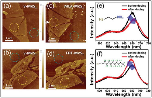
A similar approach for the passivation of sulfur vacancies in monolayer MoS2 by (3-mercaptopropyl)trimethoxysilane (MPS) molecules was reported by Yu et al [Citation99]. Due to the presence of trimethoxy silane groups, which form SAMs on SiO2 as discussed in the earlier sections, functionalization of MoS2 from the bottom was also possible. Transport characteristics from back-gated FET using functionalized MoS2 as channel samples showed an increase in room temperature field effect mobility up to ~80 cm2 V−1 S−1. Similar studies carried out by Cho et al. on chemisorbed alkanethiol molecules on multilayered MoS2 showed a shift in Raman spectra, PL spectra and a decrease in channel current in FETs [Citation100]. The observed decrease in the channel current was attributed to the passivation of SV sites by alkanethiol molecules. It was postulated that passivation of SV sites resulted in a decrease of electron hopping, which takes place via SV sites in pristine MoS2 channels. The channel current was measured for different samples with varying MoS2 thickness in order to establish a relation between the impact of alkanethiol molecules and surface–volume ratio of MoS2. These studies clearly showed the possibility of using thiol molecules to tune the electronic properties of TMDs. In this context, Sim et al. showed controlled n-type or p-type doping of MoS2 by functionalization with thiol molecules containing donor or acceptor groups [Citation22]. Using thermal annealing, additional SV sites were created in MoS2 which were then functionalized by mercaptoethylamine (MEA) and 1H,1H,2H,2H-perfluorodecanethiol (FDT) as n-type and p-type dopant, respectively. Covalent functionalization of MoS2 was confirmed using XPS analysis of C1s and N1s core level spectra. PL measurements showed a redshift for MEA-MoS2 and blue shift for FDT-MoS2, suggesting n-type and p-type doping, respectively ()). XPS results were supported by AFM measurements, which show a clear modification of the MoS2 flakes after functionalization ((a–d)). The doping effect was also observed by transfer characteristics measured by FET devices. However, the doping effect became much more evident after thermal annealing of the samples at 150°C for 10 min, which possibly removed water and oxygen form the surface.
Figure 17. (a,b) AFM images of 4-layer MoS2 after thermal annealing on a SiO2/Si substrate. (c,d) AFM images of the same MoS2 samples after the doping process using MEA and FDT, respectively. The surface roughness of each sample was calculated using these AFM images collected from the blue circle (substrate) and yellow circle (MoS2 surface). PL spectra of functionalized MoS2 before and after doping process; (e) n-doping phenomenon (MEA), (f) p-doping phenomenon (FDT). Adapted with permission from ref 22. Copyright © 2015 American Chemical Society.
Covalent functionalization of hBN and black phosphorus
Compared to graphene chemistry covalent functionalization of hBN is not extensively studied, due to its perceived inert nature. However, there are still some studies which show covalent chemical functionalization of hBN nanosheets. Lin et al. showed the covalent attachment of octadecylamine (ODA) on the defect sites of hBN nanoflakes [Citation101]. To enhance the grafting density of ODA molecules, additional defects were created in the hBN flakes. TGA measurements confirmed the impact of these additional defect sites on the grafting efficiency on hBN. A signature for amine–boron interactions was observed by NMR spectroscopy. Another approach of covalent functionalization of hBN is solution phase oxygen radical functionalization of boron atoms as demonstrated by Sainsbury et al [Citation102]. In this two-step approach, first the hBN nanosheets are reacted with tert-butoxy radicals which results in the formation of boronate ester bonds C-O-B with boron atoms in the lattice. This forms a chemical handle at the surface which is susceptible to hydrolysis and thus can be used to graft other chemical species.
A more straightforward approach for covalent functionalization of hBN nanosheets was demonstrated by Coleman and coworkers [Citation103]. Covalent functionalization by nitrene groups was carried out by first attaching an organo‐azide precursor, 4‐methoxybenzyloxycarbonyl azide, which upon thermolysis creates nitrene groups which attach to boron atoms in the hBN lattice.
Kumar et al. have recently studied molecular doping of hBN nanoflakes by TCNQ molecules [Citation104]. UV-vis and PL spectra showed the emergence of new peaks for TCNQ functionalized hBN nanoflakes. On further investigation, it was found that an oxidative decay product of TCNQ, namely α,α-dicyano-p-toluoylcyanide (DCTC), was responsible for new UV-vis peaks and PL peak in the red region. DFT calculations revealed that hybridization between the N atomic states of hBN flakes with boron vacancy (hBN-VB) and DCTC molecular orbitals resulted in new states at 1.8eV and 1.96eV. Upon excitation, an electron transfer from these states to the LUMO of DCTC molecules leads to emission peaks at ~616 nm and ~672 nm. These studies show that a charge transfer process between the mid-gap states, resulting from hybridization between molecules, and defect sites of the substrates can also lead to a modification in the optoelectronic properties of 2D materials.
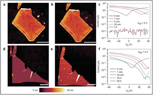
Aryl diazonium based covalent functionalization of black phosphorus was recently reported by Hersam and coworkers [Citation105]. BP flakes prepared by mechanical exfoliation on SiO2/Si wafers were immersed in a solution of 4-nitrobenzene-diazonium (4-NBD) or 4-methoxylbenzene-diazonium (4-MBD). The immersion time had a profound impact on the degree of functionalization. Topographical images by AFM showed an increase in the thickness of BP flakes form 7 nm to 8.3 nm after functionalization. Peaks corresponding to P-C bonds were observed by XPS spectroscopy, confirming the covalent functionalization of diazonium molecules. BP flakes functionalized by 4-NBD molecules showed very little or no change in morphology even after 10 days in ambient conditions, confirming the passivating effect of grafted diazonium species as shown in ). Transfer characteristics confirmed the electron transfer from BP flakes to NBD molecules resulting in p-type doping of BP flakes as shown in ).
Figure 18. AFM characterization of BP morphology before and after ambient exposure. (a) BP flake immediately after functionalization with 10 mM 4-NBD for 30 min. (b) The same flake as in a after 10 days of ambient exposure. (d) Pristine BP flake immediately after exfoliation. (e) The same flake as in d after 10 days of ambient exposure has distinct morphological protrusions indicative of chemical degradation. (c) Transfer curves for an exfoliated BP FET as a function of exposure time to 10 mM 4-NBD demonstrate strong p-type doping and show a loss of conduction. VDS, drain-source voltage. (f) Transfer curves for an exfoliated BP FET as a function of exposure time to 1 μM 4-NBD. Adapted with permission from ref 105. Copyright © 2016 Nature Publishing Group.
van Druenen et al. have recently reported another method for functionalization of liquid exfoliated BP nanoflakes by aryliodonium salts [Citation106]. This method, when compared to using aryl diazonium salts, showed better stability. BP flakes were obtained by liquid phase exfoliation in anhydrous N-methyl pyrrolidone (NMP) and acetonitrile (ACN) and functionalized by bis(4-fluorophenyl)iodonium triflate (FPI), (perfluoro-n-propyl)phenyliodonium triflate (PPI) or bis(4-methylphenyl)iodonium hexfluorophosphate (MPI), respectively. The functionalized samples were characterized by SEM, TEM, XPS, FT-IR and Raman spectroscopy. Covalent functionalization of iodonium salts on BP flakes was confirmed by C1s, F1s, and I3d core level spectra by XPS.
Conclusions and outlook
In the first part, highlighting non-covalent functionalization strategies, we focused on supramolecular chemistry-based approaches towards engineering the electronic band structure of 2D materials. Charge transfer doping by self-assembled molecules provides an alternative to substitutional doping towards controlled doping of 2D materials. Organic molecules with electron donating or withdrawing functional groups can be used for inducing n-type or p-type doping in 2D materials. This approach is highly versatile as there is a vast library of functional groups and organic molecules that can be synthesized depending on the nature of the 2D material and the extent of doping required, and can be utilized for the bottom-up synthesis of van der Waals heterostructures with 2D materials. SAMNs can induce a periodic potential modulation which can result in profound modification of electronic band structure. In the case of TMD functionalization, this may also lead to superior transport characteristics and strong photoluminescence yield. Additionally, self-assembled molecules can be used as passivating layers for highly unstable 2D materials like black phosphorus and some TMDs.
Covalent functionalization is an interesting approach which is more robust and leads to a strong modification of the electronic properties of 2D materials. We have discussed the most prominent chemistries for functionalization of graphene and other 2D materials. The strong concerns over the randomness of the covalent chemistry approach have very recently been addressed by combining it with SAMN templating, resulting in patterned grafting on 2D materials. This approach allows a better control over the density and the extent of grafting. Covalent chemistry also allows attaching functional groups to 2D materials, which are sensitive towards different organic and inorganic species, therefore realizing the potential of 2D materials in sensors.
Finally, we have stressed the fact that SPM-based methods are critical in studying the impact of molecular functionalization on the properties of 2D materials. These techniques result in acquiring atomically or sub-molecular-resolved images of the molecule-2D material systems. Beyond providing structural information, scanning probe-based spectroscopy approaches, such as STS and KPFM, are also highly useful in studying the modulation in the electronic band structure of 2D materials interacting with molecules.
Non-covalent and covalent functionalization approaches of 2D materials such as graphene, TMDs, BP and hBN are highly promising methods for the controlled modification of a number of properties such as dispersion in solutions, tuning of the electronic band structure and transport properties. Although the functionalization of graphene and TMDs is well established, the development of functionalization strategies for other 2D materials such as BP and hBN is still ongoing. A number of fundamental challenges such as the development of suitable characterization methods, improving the interactions between molecules and target materials and the reactivity of 2D materials towards various functionalizing compounds remain to be addressed to obtain well-controlled chemical activation strategies for 2D materials. Chemical modification of 2D materials using molecules and assemblies of molecules is not only a promising alternative to other approaches aiming at controlling the (opto)electronic properties of 2D materials, the huge range of compounds and chemistries that can be used for functionalization further offers almost endless opportunities to modify and engineer the properties of 2D materials. New functionalities added in 2D materials using chemical approaches can open up possibilities towards the development of multifunctional materials. As discussed in this review, 2D materials can be functionalized by photo-switchable, electrochemically switchable and magneto-responsive molecules, which can be activated by external stimuli. A controlled activation of molecules at the interface of 2D materials will result in tuning the electronic, chemical and magnetic properties of these materials with much higher control. A systematic control over the degree and site of functionalization would result in better control over the optoelectronic properties of 2D materials. Finally, encapsulation of molecule-2D material hybrid structures must be studied in order to improve the long-term stability of devices based on these hybrids.
Acknowledgments
This work has received funding from the Fund of Scientific Research–Flanders (FWO), KU Leuven Internal Funds, and the European Research Council under the European Union’s Seventh Framework Programme (FP7/2007-2013)/ERC Grant Agreement No. 340324. J. S. acknowledges financial support through a Marie Skłodowska-Curie Individual Fellowship (EU project 789865 - EnSurf).
Disclosure statement
No potential conflict of interest was reported by the authors.
Additional information
Funding
References
- Geim AK, Novoselov KS. The rise of graphene. Nat Mater. 2007;6:451.
- Georgakilas V, Otyepka M, Bourlinos AB, et al. Functionalization of graphene: covalent and non-covalent approaches, derivatives and applications. Chem Rev. 2012;112:6156–489.
- Liu H, Liu Y, Zhu D. Chemical doping of graphene. J Mater Chem. 2011;21:3335–3345.
- Loh KP, Bao Q, Ang PK, et al. The chemistry of graphene. J Mater Chem. 2010;20:2277–2289.
- Mali KS, Greenwood J, Adisoejoso J, et al. Nanostructuring graphene for controlled and reproducible functionalization. Nanoscale. 2015;7:1566–1585.
- Lv R, Li Q, Botello-Méndez AR, et al. A Peptide/MHCII conformer generated in the presence of exchange peptide is substrate for HLA-DM editing. Sci Rep. 2012;2:586.
- Daukiya L, Nair MN, Cranney M, et al., Functionalization of 2D materials by intercalation. Prog Surf Sci. 2019, 94: 1-20.
- Li B, Klekachev AV, Cantoro M, et al. Toward tunable doping in graphene FETs by molecular self-assembled monolayers. Nanoscale. 2013;5:9640–9644.
- Park J, Yan M. Covalent Functionalization of Graphene with Reactive Intermediates. Acc Chem Res. 2013;46:181–189.
- Niyogi S, Bekyarova E, Itkis ME, et al. Spectroscopy of covalently functionalized graphene. Nano Lett. 2010;10:4061–4066.
- Sarkar S, Bekyarova E, Haddon RC. Covalent chemistry in graphene electronics. Mater Today. 2012;15:276–285.
- Greenwood J, Phan TH, Fujita Y, et al. Covalent modification of graphene and graphite using diazonium chemistry: tunable grafting and nanomanipulation. ACS Nano. 2015;9:5520–5535.
- Daukiya L, Mattioli C, Aubel D, et al. Covalent functionalization by cycloaddition reactions of pristine defect-free graphene. ACS Nano. 2017;11:627–634.
- Chhowalla M, Shin HS, Eda G, et al. The chemistry of two-dimensional layered transition metal dichalcogenide nanosheets. Nat Chem. 2013;5:263.
- Lv R, Robinson JA, Schaak RE, et al. Transition metal dichalcogenides and beyond: synthesis, properties, and applications of single- and few-layer nanosheets. Acc Chem Res. 2015;48:56–64.
- Manzeli S, Ovchinnikov D, Pasquier D, et al. 2D transition metal dichalcogenides. Nat Rev Mater. 2017;2:17033.
- Zhao Y, Xu K, Pan F, et al. Doping, contact and interface engineering of two-dimensional layered transition metal dichalcogenides transistors. Adv Funct Mater. 2017;27:1603484.
- Chen X, Berner NC, Backes C, et al. Functionalization of Two‐Dimensional MoS2: On the Reaction Between MoS2 and Organic Thiols. Angew Chem Int Ed. 2016;55:5803–5808.
- Canton-Vitoria R, Sayed-Ahmad Baraza Y, Pelaez-Fernandez M, et al. Functionalization of MoS2 with 1,2-dithiolanes: toward donor-acceptor nanohybrids for energy conversion. npj 2D Materials and Applications. 2017; Vol. 1. :, Number 13.
- Ding Q, Czech KJ, Zhao Y, et al. ACS Appl Mater Interfaces. 2017;9:12734–12742.
- Presolski S, Wang L, Loo AH, et al. Functional nanosheet synthons by covalent modification of transition-metal dichalcogenides. Chem Mater. 2017;29:2066–2073.
- Sim DM, Kim M, Yim S, et al. Controlled doping of vacancy-containing few-layer MoS2 via highly stable thiol-based molecular chemisorption. ACS Nano. 2015;9:12115–12123.
- Chou SS, De M, Kim J, et al. Ligand conjugation of chemically exfoliated MoS2. J Am Chem Soc. 2013;135:4584–4587.
- Makarova M, Okawa Y, Aono M. J Phys Chem C. 2012;116:22411–22416.
- Tuxen A, Kibsgaard J, Gøbel H, et al. Size threshold in the dibenzothiophene adsorption on MoS2 nanoclusters. ACS Nano. 2010;4:4677–4682.
- Knirsch KC, Berner NC, Nerl HC, et al. Basal-plane functionalization of chemically exfoliated molybdenum disulfide by diazonium salts. ACS Nano. 2015;9:6018–6030.
- Chu XS, Yousaf A, Li DO, et al. Direct covalent chemical functionalization of unmodified two-dimensional molybdenum disulfide. Chem Mater. 2018;30:2112–2128.
- Vishnoi P, Sampath A, Waghmare UV, et al. Covalent Functionalization of Nanosheets of MoS2 and MoSe2 by Substituted Benzenes and Other Organic Molecules. Chem Eur J. 2017;23:886–895.
- Voiry D, Goswami A, Kappera R, et al. Covalent functionalization of monolayered transition metal dichalcogenides by phase engineering. Nat Chem. 2014;7:45.
- Bertolazzi S, Gobbi M, Zhao Y, et al. Molecular chemistry approaches for tuning the properties of two-dimensional transition metal dichalcogenides. Chem Soc Rev. 2018;47:6845–6888.
- Goronzy DP, Ebrahimi M, Rosei F, et al. Supramolecular assemblies on surfaces: nanopatterning, functionality, and reactivity. ACS Nano. 2018;12:7445–7481.
- Wang QH, Hersam MC. Room-temperature molecular-resolution characterization of self-assembled organic monolayers on epitaxial graphene. Nat Chem. 2009;1:206.
- Huang H, Chen S, Gao X, et al. Structural and electronic properties of PTCDA thin films on epitaxial graphene. ACS Nano. 2009;3:3431–3436.
- Lauffer P, Emtsev KV, Graupner R, et al. Molecular and electronic structure of PTCDA on bilayer graphene on SiC(0001) studied with scanning tunneling microscopy. Phys Status Solidi B. 2008;245:2064–2067.
- Karmel HJ, Garramone JJ, Emery JD, et al. Self-assembled organic monolayers on epitaxial graphene with enhanced structural and thermal stability. Chem Comm. 2014;50:8852–8855.
- Barja S, Garnica M, Hinarejos JJ, et al. Self-organization of electron acceptor molecules on graphene. Chem Comm. 2010;46:8198–8200.
- Stradi D, Garnica M, Díaz C, et al. Controlling the spatial arrangement of organic magnetic anions adsorbed on epitaxial graphene on Ru(0001). Nanoscale. 2014;6:15271–15279.
- Chen W, Chen S, Qi DC, et al. Surface transfer p-type doping of epitaxial graphene. J Am Chem Soc. 2007;129:10418–10422.
- Mao J, Zhang H, Jiang Y, et al. Tunability of supramolecular Kagome lattices of magnetic phthalocyanines using graphene-based moire patterns as templates. J Am Chem Soc. 2009;131:14136–14137.
- Yang K, Xiao WD, Jiang YH, et al. Molecule–substrate coupling between metal phthalocyanines and epitaxial graphene grown on Ru(0001) and Pt(111). J Phys Chem C. 2012;116:14052–14056.
- Ogawa Y, Niu T, Wong SL, et al. Self-assembly of polar phthalocyanine molecules on graphene grown by chemical vapor deposition. J Phys Chem C. 2013;117:21849–21855.
- Zhang HG, Sun JT, Low T, et al. Assembly of iron phthalocyanine and pentacene molecules on a graphene monolayer grown on Ru(0001). Phys Rev B. 2011;84:245436.
- Scardamaglia M, Lisi S, Lizzit S, et al. Graphene-induced substrate decoupling and ideal doping of a self-assembled iron-phthalocyanine single layer. J Phys Chem C. 2013;117:3019–3027.
- Phillipson R, Lockhart de la Rosa CJ, Teyssandier J, et al. Tunable doping of graphene by using physisorbed self-assembled networks. Nanoscale. 2016;8:20017–20026.
- Prado MC, Nascimento R, Moura LG, et al. Two-dimensional molecular crystals of phosphonic acids on graphene. ACS Nano. 2011;5:394–398.
- Gobbi M, Bonacchi S, Lian JX, et al. Periodic potentials in hybrid van der Waals heterostructures formed by supramolecular lattices on graphene. Nat Commun. 2017;8:14767.
- Gobbi M, Bonacchi S, Lian JX, et al. Collective molecular switching in hybrid superlattices for light-modulated two-dimensional electronics. Nat Commun. 2018;9:2661.
- Hara M, Iwakabe Y, Tochigi K, et al. Anchoring structure of smectic liquid-crystal layers on MoS2 observed by scanning tunnelling microscopy. Nature. 1990;344:228.
- Cincotti S, Rabe JP. Self-assembled alkane monolayers on MoSe2. and MoS2 Appl Phys Lett. 1993;62:3531–3533.
- Schreiber F. Structure and growth of self-assembling monolayers. Prog Surf Sci. 2000;65:151–257.
- Love JC, Estroff LA, Kriebel JK, et al. Self-assembled monolayers of thiolates on metals as a form of nanotechnology. Chem Rev. 2005;105:1103–1170.
- Wang J, Yu H, Zhou X, et al.. Nat Commun. 2017;8:377.
- Li Y, Xu C-Y, Hu P, et al. ACS Nano. 2013;7:7795–7804.
- Lee WH, Park YD. Tuning electrical properties of 2D materials by self-assembled monolayers. Adv Mater Interfaces. 2018;5:1700316.
- Cheng L, Lee J, Zhu H, et al. Sub-10 nm tunable hybrid dielectric engineering on MoS2 for two-dimensional material-based devices. ACS Nano. 2017;11:10243–10252.
- Kang D-H, Shim J, Jang SK, et al. Controllable Nondegenerate p-Type Doping of Tungsten Diselenide by Octadecyltrichlorosilane. ACS Nano. 2015;9:1099–1107.
- Kang D-H, Kim M-S, Shim J, et al. High-performance transition metal dichalcogenide photodetectors enhanced by self-assembled monolayer doping. Adv Funct Mater. 2015;25:4219–4227.
- Li J, Wierzbowski J, Ceylan Ö, et al. Appl Phys Lett. 2014;105:241116.
- Rosa CJLDL, Phillipson R, Teyssandier J, et al. Appl Phys Lett. 2016;109:253112.
- Kiriya D, Tosun M, Zhao P, et al. Air-stable surface charge transfer doping of MoS₂ by benzyl viologen. J Am Chem Soc. 2014;136:7853–7856.
- Mouri S, Miyauchi Y, Matsuda K. Tunable photoluminescence of monolayer MoS₂ via chemical doping. Nano Lett. 2013;13:5944–5948.
- Wang J, Ji Z, Yang G, et al. Charge Transfer within the F4TCNQ‐MoS2 van der Waals Interface: Toward Electrical Properties Tuning and Gas Sensing Application. Adv Funct Mater. 2018, 28:1806244.
- Molina-Mendoza AJ, Vaquero-Garzon L, Leret S, et al. Engineering the optoelectronic properties of MoS2 photodetectors through reversible noncovalent functionalization. Chem Comm. 2016;52:14365–14368.
- Auwärter W. Hexagonal boron nitride monolayers on metal supports: Versatile templates for atoms, molecules and nanostructures. Surface Science Reports. 2018, 74: 1-95.
- Schulz F, Drost R, Hämäläinen SK, et al. Templated self-assembly and local doping of molecules on epitaxial hexagonal boron nitride. ACS Nano. 2013;7:11121–11128.
- Abellán G, Lloret V, Mundloch U, et al. Noncovalent functionalization of black phosphorus. Angew Chem Int Ed. 2016;55:14557–14562.
- Abellán G, Wild S, Lloret V, et al. fundamental insights into the degradation and stabilization of thin layer black phosphorus. J Am Chem Soc. 2017;139:10432–10440.
- Korolkov VV, Timokhin IG, Haubrichs R, et al. Supramolecular networks stabilise and functionalise black phosphorus. Nat Commun. 2017;8:1385.
- Han C, Hu Z, Gomes LC, et al. Surface Functionalization of Black Phosphorus via Potassium toward High-Performance Complementary Devices. Nano Lett. 2017;17:4122–4129.
- Bekyarova E, Itkis ME, Ramesh P, et al. Chemical Modification of Epitaxial Graphene: Spontaneous Grafting of Aryl Groups J Am Chem Soc. 2009;131:1336–1337.
- Sinitskii A, Dimiev A, Corley DA, et al. Kinetics of Diazonium Functionalization of Chemically Converted Graphene Nanoribbons. ACS Nano. 2010;4:1949–1954.
- Sharma R, Baik JH, Perera CJ, et al. Anomalously Large Reactivity of Single Graphene Layers and Edges toward Electron Transfer Chemistries. Nano Lett. 2010;10:398–405.
- Huang P, Zhu H, Jing L, et al. Graphene Covalently Binding Aryl Groups: Conductivity Increases Rather than Decreases. ACS Nano. 2011;5:7945–7949.
- Paulus GLC, Wang QH, Strano MS. Covalent Electron Transfer Chemistry of Graphene with Diazonium Salts. Acc Chem Res. 2013;46:160–170.
- Wang QH, Jin Z, Kim KK, et al. Understanding and controlling the substrate effect on graphene electron-transfer chemistry via reactivity imprint lithography. Nat Chem. 2012;4:724.
- Shih C-J, Wang QH, Jin Z, et al. Disorder Imposed Limits of Mono- and Bilayer Graphene Electronic Modification Using Covalent Chemistry. Nano Lett. 2013;13:809–817.
- Sarkar S, Bekyarova E, Niyogi S, et al. Diels-Alder chemistry of graphite and graphene: graphene as diene and dienophile. J Am Chem Soc. 2011;133:3324–3327.
- Li J, Li M, Zhou -L-L, et al. Click and Patterned Functionalization of Graphene by Diels–Alder Reaction. J Am Chem Soc. 2016;138:7448–7451.
- Sarkar S, Bekyarova E, Haddon RC. Chemistry at the Dirac Point: Diels–Alder Reactivity of Graphene. Acc Chem Res. 2012;45:673–682.
- Bian S, Scott AM, Cao Y, et al. Covalently Patterned Graphene Surfaces by a Force-Accelerated Diels–Alder Reaction. J Am Chem Soc. 2013;135:9240–9243.
- Zhong X, Jin J, Li S, et al. Aryne cycloaddition: highly efficient chemical modification of graphene. Chem Comm. 2010;46:7340–7342.
- Zhong X, Yu H, Zhuang G, et al. Pyridyne cycloaddition of graphene: “external” active sites for oxygen reduction reaction. J Mater Chem A. 2014;2:897–901.
- Choi J, Kim K-J, Kim B, et al. Covalent Functionalization of Epitaxial Graphene by Azidotrimethylsilane. J Phys Chem C. 2009;113:9433–9435.
- Strom TA, Dillon EP, Hamilton CE, et al. Nitrene addition to exfoliated graphene: a one-step route to highly functionalized graphene. Chem Comm. 2010;46:4097–4099.
- Chua CK, Ambrosi A, Pumera M. Introducing dichlorocarbene in graphene. Chem Comm. 2012;48:5376–5378.
- Niyogi S, Bekyarova E, Hong J, et al. Covalent Chemistry for Graphene Electronics. J Phys Chem Lett. 2011;2:2487–2498.
- Hossain MZ, Walsh MA, Hersam MC. Scanning Tunneling Microscopy, Spectroscopy, and Nanolithography of Epitaxial Graphene Chemically Modified with Aryl Moieties. J Am Chem Soc. 2010;132:15399–15403.
- Kaplan A, Yuan Z, Benck JD, et al. Current and future directions in electron transfer chemistry of graphene. Chem Soc Rev. 2017;46:4530–4571.
- Xia Z, Leonardi F, Gobbi M, et al. Electrochemical Functionalization of Graphene at the Nanoscale with Self-Assembling Diazonium Salts. ACS Nano. 2016;10:7125–7134.
- Tahara K, Ishikawa T, Hirsch BE, et al. Self-Assembled Monolayers as Templates for Linearly Nanopatterned Covalent Chemical Functionalization of Graphite and Graphene Surfaces. ACS Nano. 2018;12:11520–11528.
- Bueno RA, Martínez JI, Luccas RF, et al. Highly selective covalent organic functionalizationof epitaxial graphene. Nat Commun. 2017;8:15306.
- Altenburg SJ, Lattelais M, Wang B, et al. Reaction of Phthalocyanines with Graphene on Ir(111). J Am Chem Soc. 2015;137:9452–9458.
- Kumar A, Banerjee K, Dvorak M, et al. Charge-Transfer-Driven Nonplanar Adsorption of F4TCNQ Molecules on Epitaxial Graphene. ACS Nano. 2017;11:4960–4968.
- Jacobsen A, Koehler FM, Stark WJ, et al. Towards electron transport measurements in chemically modified graphene: effect of a solvent. New J Phys. 2010;12:125007.
- Zhang H, Bekyarova E, Huang J-W, et al. Aryl Functionalization as a Route to Band Gap Engineering in Single Layer Graphene Devices. Nano Lett. 2011;11:4047–4051.
- Backes C, Berner NC, Chen X, et al. Functionalization of Liquid-Exfoliated Two-Dimensional 2H-MoS2. Angew Chem Int Ed. 2015;54:2638–2642.
- Cai M, Zhang F, Zhang C, et al. Cobaloxime anchored MoS2 nanosheets as electrocatalysts for the hydrogen evolution reaction. J Mater Chem A. 2018;6:138–144.
- Chen X, McAteer D, McGuinness C, et al. RuII Photosensitizer‐Functionalized Two‐Dimensional MoS2 for Light‐Driven Hydrogen Evolution. Chem Eur J. 2018;24:351–355.
- Yu Z, Pan Y, Shen Y, et al. Towards intrinsic charge transport in monolayer molybdenum disulfide by defect and interface engineering. Nat Commun. 2014;5:5290.
- Cho K, Min M, Kim T-Y, et al. Electrical and optical characterization of MoS2 with sulfur vacancy passivation by treatment with alkanethiol molecules. ACS Nano. 2015;9:8044–8053.
- Lin Y, Williams TV, Cao W, et al. Defect functionalization of hexagonal boron nitride nanosheets. J Phys Chem C. 2010;114:17434–17439.
- Sainsbury T, Satti A, May P, et al. Oxygen radical functionalization of boron nitride nanosheets. J Am Chem Soc. 2012;134:18758–18771.
- Sainsbury T, Satti A, May P, et al. Covalently functionalized hexagonal boron nitride nanosheets by nitrene addition. Chem Eur J. 2012;18:10808–10812.
- Kumar V, Joshi N, Dhara B, et al. Stable red emission from nanosheets of molecularly doped hexagonal boron nitride. J Phys Chem C. 2018;122:21076–21082.
- Ryder CR, Wood JD, Wells SA, et al. Covalent functionalization and passivation of exfoliated black phosphorus via aryl diazonium chemistry. Nat Chem. 2016;8:597.
- van Druenen M, Davitt F, Collins T, et al. Covalent functionalization of few-layer black phosphorus using iodonium salts and comparison to diazonium modified black phosphorus. Chem Mater. 2018;30:4667–4674.