
 ?Mathematical formulae have been encoded as MathML and are displayed in this HTML version using MathJax in order to improve their display. Uncheck the box to turn MathJax off. This feature requires Javascript. Click on a formula to zoom.
ABSTRACT
Advances in two-dimensional (2D) materials research have opened up new opportunities in miniaturization of optoelectronic and spintronic devices at the atomically thin limit. One major research thrust, which is the subject of this review, is the surface- and electronic structure of 2D materials and their van der Waals (vdW) heterostructures that may be significantly affected by the local atomic geometry and environment. As a result, there is a pressing need for powerful advanced microscopy and spectroscopy techniques for material characterization at a micro- or sub-micrometer lateral scale, which is a typical sample size in many 2D-materials experiments. Spectroscopic photoemission and low-energy electron microscopy (SPE-LEEM) offer a multifunctional approach that uniquely integrates microscopy, diffraction and spectroscopy techniques, enables real-time imaging and in situ structural, chemical and electronic analysis of surfaces and interfaces. This review covers the recent developments in SPE-LEEM investigations of surface- and electronic structure of 2D materials, and presents examples including exfoliated vdW layered materials, vdW heterostructures, and thin films synthesized by chemical vapor deposition and molecular beam epitaxy.
Graphical Abstract
1. Introduction
1.1. Background
The discovery of graphene in 2004 has demonstrated that reducing the dimensionality of a crystal down to its two-dimensional (2D) limit can yield novel electrical and optical properties [Citation1–Citation4]. This discovery immediately sparked an intense interest in searching and exploring new 2D systems. Over the past 10 years, the research in 2D materials has expanded to include a large and diverse family of materials [Citation5–Citation10]. The most studied 2D materials beyond graphene include transition metal dichalcogenides (TMDC) MX2 (M = Mo, W; X = S, Se) [Citation11–Citation14], hexagonal boron nitride (hBN) [Citation15], and black phosphorous (BP) [Citation16–Citation21]. These layered van der Waals (vdW) materials have strong in-plane chemical bonds and weak interlayer interactions. As a result, they can be easily fabricated to atomically thin sheets using mechanical exfoliation [Citation2], and these isolated 2D atomic planes can be flexibly stacked to make artificial structures such as twisted bilayers [Citation22,Citation23] and vdW heterostructures [Citation24–Citation28]. Going beyond exfoliation from naturally occurring layered materials, entirely synthetic elemental 2D materials represent an alternative route for the discovery of new 2D materials, which have no known bulk analogues [Citation29,Citation30]. Successful synthesis of elemental 2D materials has been realized in several group III-V elements on various substrates. Very recently, ferroic orders in the 2D limit has emerged as a new frontier of 2D materials research [Citation31–Citation33]. Exciting developments have been made such as demonstration of 2D ferroelectricity in monochalcogenides [Citation34,Citation35] and 2D magnetism in magnetic vdW materials [Citation36–Citation43]. These advances open up new opportunities for exploring 2D spintronics. In the meantime, monochalcogenides and magnetic vdW crystals hold the promise of becoming new building blocks for vdW heterostructures.
The diversity and tunability of 2D materials can be exploited in a wide variety of optoelectronics and spintronics applications. The 2D materials family includes semimetals, semiconductors, and insulators, which provide a wide choice of bandgaps. The range of bandgaps can be further expanded by application of strain, alloying and electric field gating. Besides the wide range of bandgap, the electronic structure of many 2D materials displays topological nontrivial properties. In fact, electronic structure is of crucial importance for understanding the striking physical properties of 2D materials. Angle-resolved photoemission spectroscopy (ARPES) is one of the most direct experimental techniques for studying the electronic band structure of crystals with high momentum resolution [Citation44–Citation46]. Important properties of the electronic structure can be extracted from ARPES measurements including energy position of the band edge, effective mass, Fermi velocity, doping evolution, and electron self-energy, which is tied to many body effects. However, in applying standard ARPES measurements to 2D materials, there are two main challenges to be overcome; one limitation is sample size, the other is its environment. First, the lateral dimension of the exfoliated 2D flakes is commonly limited to micrometer length scales; hence the measurement of these small flakes of 2D materials requires an extremely small beam spot size, i.e. 2–5 m. While chemical vapor deposition (CVD) [Citation47,Citation48] and molecular beam epitaxy (MBE) [Citation49] techniques can now be used to grow large 2D thin films, however, due to the multidomain nature of many 2D material systems, local-probe ARPES is also extremely useful in studying the electronic structure within a single domain. Second, 2D flakes are highly sensitive to the local geometry and environment. In this case, the electronic structure of 2D materials is tightly correlated to their surface structure. To obtain an intrinsic electronic structure, it is essential to have a clean and defect- and wrinkle-free surface on the 2D flakes.
Speaking more generally, an ideal apparatus for studying surface and electronic structures of 2D materials should allow (i) real-time visualization of the samples with high spatial resolution; (ii) surface-sensitive characterization of the local crystalline structure; (iii) chemical sensitivity of surface adsorption or contaminations; and (iv) a micrometer sampling area for acquiring ARPES data.
Spectroscopic photoemission and low-energy electron microscopy (SPE-LEEM) [Citation50] matches the particular requirements listed above. The SPE-LEEM instrument, which is the heart of the measurements discussed in this paper, accomplishes this by combining microscopy, diffraction, and spectroscopy in one experimental setup. The experiments are carried out in conjunction with the bright and broad spectrum of synchrotron radiation light source [Citation51–Citation59]. SPE-LEEM was developed in 1980s, and the current commercial instruments can be found in most of the major synchrotron facilities. This versatile instrument has been extensively used for in situ dynamic studies of surface processes such as growth, decomposition, melting, phase transition, diffusion, doping, intercalation, etc. SPE-LEEM techniques and methods grown with widespread use of SPE-LEEM in the area of 2D materials research over the past decade. A typical SPE-LEEM study of a 2D material contains the following procedures: [label = ()]
Locate 2D flakes of interest on the substrates using low-energy electron microscopy (LEEM) employing a complete field of view
Characterize local crystalline structure using selected-area low-energy electron diffraction (
-LEED) pattern and intensity-voltage (I-V) curves
Examine, with nanometer spatial resolution, the chemical composition of the surface using photoemission electron microscopy (PEEM)
Acquire ARPES data from selected areas on the 2D flakes (
From such a study, comprehensive information on the surface and electronic structure of 2D materials can be extracted – all at high spatial resolution.
1.2. Overview of presentation
In this review article, we present selected key measurements obtained through SPE-LEEM studies of 2D materials. In Section 2, the principles of SPE-LEEM are first presented. Subsequently, a local crystalline structure analysis based on analysis of -LEED I-V curves and dynamical LEED calculation are introduced. In Section 3, the application of LEEM and
-LEED for studying the surface structure of a variety of 2D systems are discussed including atomic-layer thickness of CVD-grown graphene, the surface morphology of graphene, surface buckling in BP, surface termination and relaxation of MBE-grown SnSe thin films, and the interlayer twist of graphene/MoS2 heterostructures. Section 4 then highlights representative examples of the electronic structure of 2D materials and vdW heterostructures including the thickness-dependent electronic structure of MoS2, the effect of different substrates on the electronic structure of 2D overlayers, and bandgap engineering in graphene/MoS2 heterostructures. The electronic structure of CVD- and MBE-grown 2D thin films are also explained. Finally, Section 5 concludes with prospectives on advances in the instrument and the directions of 2D materials research.
2. Spectroscopic photoemission and low-energy electron microscopy
2.1. Principles of SPE-LEEM
-ARPES can be carried out by using one of two main approaches: spatially localized ARPES or SPE-LEEM. In the first, scanning photoemission microscope (SPEM) is exploited for visualization of the 2D material samples [Citation61–Citation63]. In this configuration, the lateral resolution is determined by the beam spot size. State-of-the-art spatially localized ARPES on synchrotron facilities can realize nanometer-sized beam spot [Citation64–Citation66]. The advantage of this method is that it enables high energy resolution to be achieved [Citation67–Citation75]. However, real- and momentum-space ARPES mapping are difficult, as they demands translation and rotation of either the sample stage or the electron analyzer in an ultrahigh vacuum environment [Citation63]. In comparison, SPE-LEEM approach does not excel in energy resolution (typically
200 meV). The advantage of SPE-LEEM is that it enables fast parallel imaging of the sample without scanning. In addition, tunable field of views are available in both real- and momentum-space imaging. As a result, it allows rapid identification of sample area of interest and ARPES mapping of Brillouin zone. Therefore, SPE-LEEM makes a versatile tool for fast surface and electronic structure characterization.
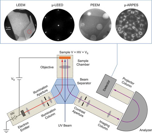
Figure 1. (a) Schematic of the Elmitec LEEM/PEEM system used for much of the SPE-LEEM studies presented here. The sample is illuminated by the incident electron beam generated from an electron emitter, deflected by the beam separator. The electrons are decelerated by the cathode lens and focused on the sample surface by an objective. The reflected electrons are reaccelerated and deflected to the imaging column. (b–e) Different imaging modes that highlight different features of the surface. Reproduced with permissions of Ref [Citation60,Citation145].
![Figure 1. (a) Schematic of the Elmitec LEEM/PEEM system used for much of the SPE-LEEM studies presented here. The sample is illuminated by the incident electron beam generated from an electron emitter, deflected by the beam separator. The electrons are decelerated by the cathode lens and focused on the sample surface by an objective. The reflected electrons are reaccelerated and deflected to the imaging column. (b–e) Different imaging modes that highlight different features of the surface. Reproduced with permissions of Ref [Citation60,Citation145].](/cms/asset/4dceace0-55c9-4d7e-ab25-6dd1b54306ab/tapx_a_1688187_f0001_oc.jpg)
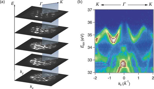
SPE-LEEM studies of 2D materials in this review are based on the Elmitec system. In particular, ) shows a schematic of the Elmitec LEEM/PEEM system. In the LEED/LEEM modes, the electrons emitted from the electron emitter are accelerated in a high voltage field (20 kV). This parallel beam of fast electrons is deflected by the electron prism and electron beam splitter. They are then decelerated to low energies (20–200 eV) at the sample surface. The reflected electrons are again accelerated towards the imaging column to generate LEED patterns or LEEM images. Bright- or dark-field images can be produced by selecting the zero-order or higher-order diffraction beam using a contrast aperture. Similarly, in the PEEM modes, the photoelectrons are used to generate images based on work function contrast. In both the LEEM/PEEM imaging modes, the size of the illuminating aperture is tuned to select a particular field of view on the sample. Furthermore, in order to carry out ARPES measurements based on a PEEM setup, a hemispherical electron analyzer must be added to the imaging column to filter the kinetic energy of the photoelectrons and generate the constant energy maps (CEMs) in the momentum space through the projector column. As shown in ), by stacking the CEMs, the electronic structure in the first Brillouin zone (BZ) is established. Vertical slices in the (,
,
) space can further show the band dispersion along high-symmetry directions of BZ, as illustrated in ). Note that besides the hemispherical electron analyzer, energy selection can be realized in different methods. For example, FOCUS PEEM with time-of-flight filter can achieve an energy resolution of the order of few tens of meV [Citation76,Citation77].
Figure 2. (a) Electronic structure of bulk MoS2 constructed in (,
,
) space one obtained by stacking constant-energy maps. (b) An ARPES band map along the
high symmetry direction as denoted by a vertical slide in (a).
2.2. LEED I-V and dynamical LEED calculations
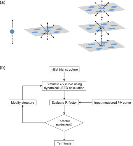
Dynamical LEED calculations based on LEED I-V analysis are a powerful approach for determining the atomic structure of the top few layers of a crystal [Citation78]. As shown in ), in the dynamical LEED calculations, electron diffraction is modeled by a multiple scattering process [Citation79,Citation80] involving three steps: (i) Scattering of the electrons by a single atom; (ii) Arranging an atomic plane to establish the diffraction matrix M(,
), where
signs indicate the incoming and outgoing directions, respectively; (iii) Stacking the atomic planes vertically to construct the total electron diffraction matrix. In the multiple scattering processes, the crystal inner potential is described using the standard muffin-tin model, in which the atomic potential is assumed to have a spherical symmetry with a finite radius and the potential between the atomic spheres is set to a constant. A self-consistent structural optimization is subsequently carried out following the workflow shown in ). In particular, an initial structure is selected and the I-V curve is calculated using a dynamical LEED formulation. The calculated I-V curve is then compared with the measured I-V curve, and the agreement between the calculated and measured I-V curve is then evaluated using a Pendry R-factor [Citation78,Citation79], which is defined as
By minimizing the R-factor in this trial-and-error procedure, a best fit of the measured I-V curve is achieved so as to obtain the optimized surface structure.
Figure 3. (a) Schematic of the three steps of the multiple scattering in dynamical LEED calculations, i.e. scattering of electrons by a single atom (left), an atomic plane (middle), and the bulk crystal (right). (b) Workflow of the self-consistent structural optimization.
3. Surface structure
3.1. Atomic layer thickness of graphene
A determination of the precise atomic layer thickness is crucial for understanding how quantities such as electronic or atomic structure vary with the number of monolayers. This thickness can be determined using a variety of ex situ techniques, including atomic force microscopy (AFM) and Raman spectroscopy [Citation81–Citation83]. While these techniques are extensively used with exfoliated graphene on different substrates, they can also be applied to other exfoliated 2D materials such as MoS2 [Citation84,Citation85]. A much more difficult challenge, however, is to determine in situ the thickness of CVD-grown graphene [Citation86–Citation88]. An excellent example of such a measurement is shown in ). In this case, LEEM I-V measurements provide a straightforward approach to determine the number of layers of graphene on Pt (111) substrate. As shown in ), the LEEM I-V curves of graphene thin films exhibits interference minima in the low-energy range between 2 and 15 eV, and each increase in number of layers gives rise to one additional interference minimum. This signature allows one to determine the thickness of graphene by simply counting the interference minima. A phase accumulation model ()), analogous to that used for metallic thin films, illustrates the interference phenomenon here. A similar observation was found in graphene on other substrates, even though in certain case, additional reflectivity minima occur depending on the graphene-substrate separation [Citation89–Citation95].
Figure 4. (a) LEEM image CVD-grown graphene on Pt (111) showing a series of thickness from 1 ML to 10 ML. (b) LEEM I-V curves with electron energy from 2 to 100 eV obtained from graphene with different layer thicknesses. (c) Magnification of the LEEM I-V curves in (b) in the low-energy range. The fringes are due to the interference of electrons backscattered from the graphene surface and graphene/Pt (111) interface. (d) Phase shifts for constructive and destructive interference as a function of electron energy. Reproduced with permission from Ref [Citation86].
![Figure 4. (a) LEEM image CVD-grown graphene on Pt (111) showing a series of thickness from 1 ML to 10 ML. (b) LEEM I-V curves with electron energy from 2 to 100 eV obtained from graphene with different layer thicknesses. (c) Magnification of the LEEM I-V curves in (b) in the low-energy range. The fringes are due to the interference of electrons backscattered from the graphene surface and graphene/Pt (111) interface. (d) Phase shifts for constructive and destructive interference as a function of electron energy. Reproduced with permission from Ref [Citation86].](/cms/asset/7c0f8f54-aafb-4ead-bc79-493445cc8e51/tapx_a_1688187_f0004_oc.jpg)
3.2. Surface morphology of 2D materials
Generically, the morphology of 2D materials is highly sensitive to the local environment of the surface. For example, 2D flakes intrinsically tend to form ripples, which can lower the surface energy [Citation96–Citation98]. Or extrinsically, substrate roughness can be transferred to the 2D membranes when they are placed on the substrate surface. In addition, at the surface where the translational symmetry along out-of-plane direction is broken, the sample surface may undergo surface reconstruction and/or surface relaxation.
Figure 5. (a–d) -LEED patterns of graphite, and trilayer (3ML), bilayer (2ML), and monolayer (1ML) graphene, respectively. (e) Intensity profiles of the central diffraction beam from (a–d). (f) Linewidth of the central diffraction beam as a function of total momentum of
-LEED electrons. Reproduced with permission from Ref [Citation99].
![Figure 5. (a–d) μ-LEED patterns of graphite, and trilayer (3ML), bilayer (2ML), and monolayer (1ML) graphene, respectively. (e) Intensity profiles of the central diffraction beam from (a–d). (f) Linewidth of the central diffraction beam as a function of total momentum of μ-LEED electrons. Reproduced with permission from Ref [Citation99].](/cms/asset/6c2b3465-7b42-4d5a-9d80-82e5999a58a8/tapx_a_1688187_f0005_oc.jpg)
The broadening of a -LEED beam can be exploited to characterize the surface roughness described above [Citation99]. A diffracted beam from an ideally flat surface will form a well-defined sharp spot with only instrumental and thermal broadening. In contrast, the diffraction beam from a corrugated surface will have additional broadening due to the surface roughness. ) show the
-LEED patterns of graphite, and 1–3 monolayers (ML) of graphene on a SiO2/Si substrate. Observe that the width of the diffraction beams increase monotonically with the decreasing thickness of the graphene layer; this phenomenon is shown clearly by the line profile of the central beam in ). Qualitatively, thicker graphene flakes are stiffer and possess a smaller magnitude of the corrugation amplitude. Quantitatively, the surface roughness can be evaluated using the following trigonometric relation
where is the standard deviation of the local surface normal,
is the Gaussian width of the central diffraction beam, and k is the total momentum of the incident electrons, which is related to the incident electron energy (
) by
. From this relation, the width of the diffraction beam can be shown to linearly increase with an increase in the momentum of the incident electrons (see )) [Citation99,Citation100]. Similar results are also obtained for the case of an exfoliated MoS2 flakes [Citation101].
Figure 6. Side view of the atomic structure of black phosphorus (a) with and (b) without surface buckling. and
denote the two P atoms in one unit cell. (c) LEEM image of exfoliated few-layer black phosphorus on Si substrate. (d)
-LEED pattern acquired from the spot denoted by the red circle in (c). (e) Measured LEED I-V curve (red dots) and calculated LEED I-V curves using the model with (green curve) and without (blue-dashed curve) surface buckling. Reproduced with permission from Ref [Citation102].
![Figure 6. Side view of the atomic structure of black phosphorus (a) with and (b) without surface buckling. P1 and P2 denote the two P atoms in one unit cell. (c) LEEM image of exfoliated few-layer black phosphorus on Si substrate. (d) μ-LEED pattern acquired from the spot denoted by the red circle in (c). (e) Measured LEED I-V curve (red dots) and calculated LEED I-V curves using the model with (green curve) and without (blue-dashed curve) surface buckling. Reproduced with permission from Ref [Citation102].](/cms/asset/a0d8d9b0-362b-4762-9572-d71e5ce09b22/tapx_a_1688187_f0006_oc.jpg)
Another application is to determine the surface structure of an exfoliated flake or a grown thin film. An example is illustrated with BP using LEED I-V measurements and dynamical LEED calculation [Citation102]. BP crystal possesses a puckered honeycomb structure as shown in ). In a defect-free and strain-free BP flake, the two P atoms in one unit cell are equivalent. However, high-resolution scanning tunneling microscopy (STM) studies of BP flakes clearly show contrast between the two P atoms in the atomic-resolved topographic image [Citation103,Citation104], which implies geometrical height difference between the two P atoms ( and
), an indication of what is termed surface buckling (see )). Structural optimization based on LEED I-V and dynamical LEED calculations have been used to determine the magnitude of this surface buckling (defined as
and
in )).
In the experiment, an exfoliated BP flake was first characterized by a LEEM image (see )) and an -LEED pattern (see )). Subsequently, two models-with/without-considering surface buckling were applied to optimize the surface structure by fitting them to the measured I-V curve of (00) diffraction beam. As shown in ), the model, which included surface buckling, most satisfactorily fit the measured I-V curve. The fit showed a 0.3 Å surface buckling, which is one order of magnitude larger than previously reported [Citation103,Citation104]. First-principle calculations further demonstrate that the surface buckling originates from the surface vacancies and is related to the intrinsic hole doping of BP.
3.3. Surface termination and relaxation
For topological materials, the surface configuration is a crucial parameter in determining the associated Dirac topological surface states. For example, in rock-salt SnSe, which is an archetypical topological crystalline insulator [Citation105], the surface possesses hybridized double Dirac-cones in close vicinity to the X point of the
surface Brillouin zone (SBZ), while the
surface possesses four Dirac cones centered at the
and M points of the
SBZ [Citation106]. Specifically, the
surface has been intensively studied because it is a natural cleavage plane [Citation107–Citation110]. In contrast, the
surface is an unstable polar surface, and is difficult to prepare by simple cleavage. However, due to advances in MBE growth techniques, preparation of the metastable SnSe
surface has now been successfully realized [Citation111]. LEED I-V analysis is a powerful tool to explore the surface termination of SnSe thin films and reveal mechanisms for stabilizing a polar surface [Citation112].
Figure 7. Calculated LEED I-V curves of the (00) diffraction beam for an optimized Sn-terminated surface (green solid curve) and a Se-terminated surface (blue solid curve) and the measured I-V curve (red dots). Reproduced with permission from Ref [Citation112].
![Figure 7. Calculated LEED I-V curves of the (00) diffraction beam for an optimized Sn-terminated surface (green solid curve) and a Se-terminated surface (blue solid curve) and the measured I-V curve (red dots). Reproduced with permission from Ref [Citation112].](/cms/asset/29cde36c-9f9c-4aab-a861-4ec9925b9c4e/tapx_a_1688187_f0007_oc.jpg)
shows the calculated I-V curves of an optimized SnSe surface structure. The calculated Sn-terminated surface accurately reproduces the major features of the measured I-V curve, while the calculated Se-terminated surface is strikingly different from the experimental data. If the charge compensation mechanism of the polar surface is invoked for this case, a well-defined LEED pattern for the
surface first rules out the possibility of surface reconstruction. Further, our optimized surface structure demonstrates an oscillatory, contraction-expansion-contraction pattern for the structural relaxation along the polar direction. This is the first direct observation of the oscillatory structural relaxation as a charge compensation mechanism, which has been predicted by DFT calculation. Therefore, LEED I-V analysis is clearly as an effective technique to determine surface termination of epitaxially grown thin films in situ.
3.4. Interlayer twist on vdW heterostructures
In addition to homogenous 2D materials, vdW heterostructures have emerged as a novel class of materials. In these materials, the weak out-of-plane coupling allows the 2D atomic planes to be vertically stacked without the demanding requirements of the lattice matching. This class of artificial materials open up new opportunity for combining the exotic properties of the individual 2D layers. In particular, graphene/MoS2 vdW heterostructures are remarkable because of the high carrier mobility of graphene as well as the direct band gap and extremely strong light–matter interactions of MoS2. The possibility of combining the properties of graphene and MoS2 together may lead to new potential applications in field-effect transistor devices, energy harvesting materials, and memory cells. In vdW heterostructures, the interlayer coupling strength can be tuned, as in one example, by adjustment of the interlayer twist angle; thus, offering a new degree of freedom for engineering their electronic structure at interfaces.
Figure 8. LEED patterns derived from a graphene overlayer (upper plane) at 40 eV and from the MoS2 bottom layer (middle plane) at 45 eV. The diffraction spots are projected to the bottom plane to extract the interlayer twist angle . Reproduced with permission from Ref [Citation113].
![Figure 8. LEED patterns derived from a graphene overlayer (upper plane) at 40 eV and from the MoS2 bottom layer (middle plane) at 45 eV. The diffraction spots are projected to the bottom plane to extract the interlayer twist angle θ. Reproduced with permission from Ref [Citation113].](/cms/asset/c0848a24-41da-4c0e-b552-c814c5de9267/tapx_a_1688187_f0008_oc.jpg)
In order to clearly tailor the electronic structure at the interfaces, an accurate determination of the interlayer twist angle must be known. The approach to this determination varies in the literature. For example, for CVD-grown grains with certain shapes, e.g. the triangle grain boundary of MoS2, it is straightforward to determine the orientation based on the alignment of the edges of the triangles. In other cases, scanning or transmission electron microscopy, and second harmonic generation have been shown to allow the determination of crystalline orientations. Finally, -LEED measurements can be used to enable rapid surveying of local crystalline orientations. This approach is discussed below.
In our experiment, the graphene/MoS2 heterostructures are constructed by stacking a CVD-grown graphene membrane on top of a CVD-grown MoS2 membrane [Citation113]. As a result, the multiple-domains of graphene and MoS2 were randomly rotated with distinct twist angles. Further as shown in , by tuning the energy of incident electrons, -LEED patterns could be selectively extracted from the graphene overlayer or from the MoS2 bottom layer. Subsequently, by projecting the
-LEED patterns from graphene and MoS2 onto a single plane, the interlayer twist angle could be determined with an accuracy of 1 In addition, the
-LEED probe can be scanned across the sample surface to survey the local crystalline domains and acquiring
-ARPES data at the spot, which exhibited an interlayer twist angle of interest.
4. Electronic structure
4.1. Thickness-dependent electronic structure of MoS2
Many unique properties and applications of TMDCs are correlated with their electronic structure. In fact, one of the most striking examples is the significantly enhanced quantum yield of photoluminescence in monolayer MoS2 compared to that in multilayer samples [Citation11,Citation12]. This result is attributed to an indirect-to-direct band gap transition when MoS2 is thinned to its monolayer limit. In addition, note that the coupled spin-valley degree of freedom can only be realized in monolayer TMDCs since at this thickness broken inversion symmetry lifts the spin degeneracy [Citation114].
Figure 9. (a–d) Thickness-dependent electronic structure visualized by 2D curvature plots of the low-energy valence band of exfoliated monolayer, bilayer, trilayer and bulk MoS2, respectively. Red curves are the corresponding DFT calculated bands. (e) The evolution of the energy difference between the valance band maximum at and
as a function of number of layers. The theoretical results are superposed for comparison. Reproduced with permission from Ref [Citation115].
![Figure 9. (a–d) Thickness-dependent electronic structure visualized by 2D curvature plots of the low-energy valence band of exfoliated monolayer, bilayer, trilayer and bulk MoS2, respectively. Red curves are the corresponding DFT calculated bands. (e) The evolution of the energy difference between the valance band maximum at Kˉ and Γˉ as a function of number of layers. The theoretical results are superposed for comparison. Reproduced with permission from Ref [Citation115].](/cms/asset/3e5d912b-6afd-42f9-9d1e-a8542b4e6617/tapx_a_1688187_f0009_oc.jpg)
These observations suggest an investigation of the evolution of the electronic structure of TMDCs as their thickness changes. Such a thickness-dependent electronic structure of exfoliated MoS2 has been studied using SPE-LEEM setup [Citation115]. In these measurements, micrometer-scale MoS2 flakes were placed on a conducting Si substrate to eliminate charging. –) shows the first measured topmost valance band of a 1-3ML and bulk MoS2 along high symmetry direction of the SBZ. The measured bands were processed by a 2D curvature filter [Citation116] for better visualization. The measured bands agree well with the DFT-calculated bands. In particular, as the thickness decreases, the energy difference between the and
valley becomes smaller, and in the monolayer case, the valence band maximum (VBM) shifts from
point to
point. The evolution of the VBM is summarized in . This measurement has provided direct evidence of the indirect-to-direct bandgap transition in TMDCs. A similar result was later obtained in MBE-grown MoSe2 thin films using high-resolution traditional large-beam-spot ARPES [Citation49].
Here, we also highlight two important prospectives for the electronic structure studies of TMDCs. First of all, TMDCs are polymorphic in having different crystalline and electronic structures. Besides the semiconducting phase, the metallic
phases have attracted great interest due to the discovery of a large non-saturating magnetoresistance [Citation117,Citation118] and type-II Weyl fermions in bulk
-WTe2 and
-MoTe2 [Citation119–Citation121]. In fact, a series of ARPES studies of the electronic structures of
-phase WTe2 and MoTe2 in the bulk form have found evidence of topological nature of these materials [Citation122–Citation128]. Recently, SPE-LEEM has been exploited to investigate the phase engineering of TMDCs.
-LEED patterns combined with the dynamical LEED calculations of I-V curves demonstrate that a critical W alloy concentration of
triggers a phase transition from the
to the
phase in MoTe2 [Citation129]. Moreover, theoretical work predicts that
-phase TMDCs in the 2D limit may host a novel state with large-gap quantum spin Hall effect [Citation130]. A thickness-dependent investigation of the topological nature of these materials is needed.
Second, TMDCs containing transition metal elements of Ti, V, Nb, and Ta hosts several important cooperative phenomena including charge density waves and superconductivity [Citation131]. However, how the reduced dimensionality and how substrate affect these cooperative orders remain outstanding questions [Citation14,Citation132]. ARPES investigation have been carried out in MBE-grown thin films such as NbSe2 [Citation133], TaS2 [Citation134], TiSe2 [Citation135–Citation138] and VSe2 [Citation139–Citation141] to address these questions. And even more interestingly, VSe2 on certain vdW substrates also exhibits 2D magnetic order [Citation142]. To date, no consistent picture has been established and further studies, especially thickness-dependent measurement of exfoliated samples will be required.
4.2. Substrate interactions
Substrate interactions can strongly affect the physical properties and electrical performance of 2D materials. In this section, we discuss the specific case of substrate interactions on exfoliated 2D flakes. The case of 2D thin films grown on substrate will be discussion in Section 4.4. The substrate affects the electronic structure of 2D flakes in two major ways. First, any roughness in the substrate can be mechanically transferred to the ultrathin 2D flakes. As a result, structural corrugations can then give rise to distorted electronic bands, as seen in ARPES measurements. Second, any interactions between these 2D flakes and the substrate can also change the intrinsic electron structure. As an example, for the case of graphene placed on hBN, the symmetry of the A-B sublattices of graphene is broken by hBN and a finite bandgap is then opened at the Dirac point [Citation143]. In addition, the dielectric constant of the substrate plays a key role in determining the exciton binding energy and quasiparticle lifetime of 2D materials.
Figure 10. (a) Schematic of graphene suspended over patterned cavities. (b) Optical image of the suspend monolayer graphene (MLG) and few-layer graphene (FLG). (c) LEEM image of sample area of interest. Background is artistic rendering of corrugated graphene sheet. ARPES data along high-symmetry direction of BZ for (d) SiO2 substrate supported graphene ( = 90 eV), (e) suspended graphene (
= 84 eV). Reproduced with permission from Ref [Citation144].
![Figure 10. (a) Schematic of graphene suspended over patterned cavities. (b) Optical image of the suspend monolayer graphene (MLG) and few-layer graphene (FLG). (c) LEEM image of sample area of interest. Background is artistic rendering of corrugated graphene sheet. ARPES data along high-symmetry direction of BZ for (d) SiO2 substrate supported graphene (hν = 90 eV), (e) suspended graphene (hν = 84 eV). Reproduced with permission from Ref [Citation144].](/cms/asset/f3248b0b-6776-49f6-8986-987ed789ff83/tapx_a_1688187_f0010_oc.jpg)
To minimize any substrate interactions, one can place the sample over patterned cavities or trenches (see ), thus eliminating the interactions over these etched features. For example, as shown in , the suspended and supported graphene area can be directly visualized via LEEM imaging prior to the ARPES measurements [Citation144]. ARPES data of suspended and substrate-supported graphene can then be compared, as is shown in –). Due to the absence of substrate interaction, as well as in many cases reduced corrugation, the suspended graphene yields a significant improvement in data quality. In addition, note that there is a very broad and parabolically dispersing feature centered at the point at a binding energy of
6–8 eV in the supported graphene. This feature is attributed to photoemission from the SiO2 substrate. Similar results are also found in other 2D materials such as MoS2 [Citation145].
4.3. Electronic structure of van der Waals structures
Manipulating electronic structure of 2D materials at the interface of twisted bilayers or vdW heterostructures has been shown to open up new opportunities for investigating emergent phenomena and novel device applications. Even though optical and transport studies can reveal ultrafast charge transfer and interlayer exciton [Citation146–Citation148], there are important questions to be addressed by full band ARPES measurements such as this twist-angle-dependent band structure, orbital selected band hybridization, and band alignment. Traditional -ARPES studies were first reported in graphene transferred onto bulk MoS2 [Citation149], WSe2/h-BN [Citation150], and monolayer MoSe2/WSe2 [Citation151]. In addition, charge transfer between epitaxially grown MoSe2 on the few-layer graphene film was investigated using PEEM-based ARPES [Citation152]. Note that twist angle is a crucial degree of freedom in manipulating electronic structure at the interfaces of vdW structures. In the works mentioned above [Citation149–Citation152], the interlayer twist angle was determined using the constant energy map of the full Brillouin zone. Here, SPE-LEEM systems with both direct local crystalline characterization and
-ARPES instruments can provide another route to correlate the interlayer twist and electronic structure at the interfaces. shows the electronic structure at a monolayer graphene/MoS2 interface. The Fermi velocity of graphene band remains the same as that of a pristine sample. However, ARPES measurements show that as the interlayer twist angle increases from 0º to 30º, the relative energy difference between the valence band maximum at
and
point varies from approximately 200 meV to 0 meV. The results demonstrate that monolayer MoS2 in graphene/MoS2 heterostructures becomes predominantly an indirect-band-gap semiconductor due to the on-set of interlayer coupling. The direct band gap of MoS2 is restored at 30º where the interlayer coupling is reduced due to the opposite registry between graphene and MoS2 layer. This work highlights the crucial role of twist angle in tuning the physical properties of heterostructures, and provide useful guidance for electronics and optics applications using graphene/MoS2 heterostructures [Citation153,Citation154]. Twist-angle-dependent electronic structure has also been investigated in twisted bilayer MoS2 using SPE-LEEM [Citation155].
Figure 11. Electronic band structure of (a) graphene and (b) MoS2 at the interface of graphene/MoS2 heterostructure. (c) Energy difference between and
versus twist angle in the Gr/MoS2 (purple) and MoS2/Gr (green) heterostructures. Reproduced with permission from Ref [Citation113].
![Figure 11. Electronic band structure of (a) graphene and (b) MoS2 at the interface of graphene/MoS2 heterostructure. (c) Energy difference between Γˉ and Kˉ versus twist angle in the Gr/MoS2 (purple) and MoS2/Gr (green) heterostructures. Reproduced with permission from Ref [Citation113].](/cms/asset/7f17bc41-67fb-454c-a5ef-ac3fac64963f/tapx_a_1688187_f0011_oc.jpg)
In particular, we focus on van der Waals bilayers with small twist angle and/or lattice mismatch, which give rise to the interesting phenomena of moiré superlattices. The periodic moiré potential introduces new length and energy scale, which can lead to nontrivial changes in electronic band structure and topological phenomena [Citation156–Citation159]. For example, a mini Dirac point and Hofstadter butterfly pattern can emerge in graphene/boron nitride moiré superlattices [Citation160–Citation163]. Recently, correlated insulating states and unconventional superconductivity have been realized in magic angle graphene superlattices [Citation164,Citation165]. Moreover, moiré excitons have been reported in transition metal dichalcogenide heterostructure superlattices [Citation166–Citation171]. To speak in a broader sense, manipulation of electronic structure by controlling the twist angle can be generally applied to 2D layered materials, leading to an exciting field called ”twistronics” [Citation172]. SPE-LEEM is expected to play a key role in advancing this field.
4.4. Electronic structure of thin films
Figure 12. ARPES band structure of (a) Ru (0001) substrate area that is not covered by graphene, and covered by (b) monolayer graphene, (c) bilayer graphene, (d) trilayer graphene. Dashed lines are DFT calculated bands of free-standing graphene. Reproduced with permission from Ref [Citation174].
![Figure 12. ARPES band structure of (a) Ru (0001) substrate area that is not covered by graphene, and covered by (b) monolayer graphene, (c) bilayer graphene, (d) trilayer graphene. Dashed lines are DFT calculated bands of free-standing graphene. Reproduced with permission from Ref [Citation174].](/cms/asset/04b65369-64bf-4d3d-ac4a-fdf2fe98cc4e/tapx_a_1688187_f0012_oc.jpg)
Figure 13. (a) Fermi surface map of graphene island on Ir (001) at room temperature acquired using a photon energy of 40 eV. White dashed lines denote the high-symmetry direction of the 1st Brillouin zone. (b) -ARPES band dispersion along the cut across K point is indicated by the red-dashed line in (a).
is the energy position of the Dirac point determined by the intersection of the two red lines, which fit the momentum distribution curves. (c) Intensity profile along the red vertical line in (b). The Fermi level (
) was determined by fitting the cut-off to a Fermi-Dirac distribution. (d) A dark-field XPEEM image of the graphene island generated by positioning an aperture at the K point, as indicated by the red circle in (a). The image intensity is proportional to the density of states (DOS) in the vicinity of K at
. (e) Normal emission XPEEM image at
. The image intensity is proportional to the DOS at
point. (f) C 1s core level emission spectra of graphene on Ir (001), as measured at room temperature (top) and 850ºC (bottom), respectively. The thin black curves are the best fit to the Doniach-Sunjić lineshape. The spectra were acquired over a microscopically extended surface area comprising both BG and FG phases using 400 eV photons. Reproduced with permission from Ref [Citation179]. and Ref [Citation180].
![Figure 13. (a) Fermi surface map of graphene island on Ir (001) at room temperature acquired using a photon energy of 40 eV. White dashed lines denote the high-symmetry direction of the 1st Brillouin zone. (b) μ-ARPES band dispersion along the cut across K point is indicated by the red-dashed line in (a). ED is the energy position of the Dirac point determined by the intersection of the two red lines, which fit the momentum distribution curves. (c) Intensity profile along the red vertical line in (b). The Fermi level (EF) was determined by fitting the cut-off to a Fermi-Dirac distribution. (d) A dark-field XPEEM image of the graphene island generated by positioning an aperture at the K point, as indicated by the red circle in (a). The image intensity is proportional to the density of states (DOS) in the vicinity of K at EF. (e) Normal emission XPEEM image at EF. The image intensity is proportional to the DOS at Γ point. (f) C 1s core level emission spectra of graphene on Ir (001), as measured at room temperature (top) and 850ºC (bottom), respectively. The thin black curves are the best fit to the Doniach-Sunjić lineshape. The spectra were acquired over a microscopically extended surface area comprising both BG and FG phases using 400 eV photons. Reproduced with permission from Ref [Citation179]. and Ref [Citation180].](/cms/asset/875e7ec9-dfc9-4b1b-9dc5-65d388b74b99/tapx_a_1688187_f0013_oc.jpg)
The rapid imaging of LEEM allows real-time monitoring of thin-film growth. In addition, in the combination with in situ spectroscopy measurements, SPE-LEEM can provide insight into the growth mechanism and important materials properties such as crystalline orientation, electronic structure, work function, and interfacial intercalation. Among the most studied graphene on an fcc (111) and hcp (0001) transition metal surfaces [Citation173] is that of graphene on Ru (0001). This is a model system that has been complementarily studied by SPE-LEEM [Citation174]. shows the thickness-dependent electronic structure of layer-by-layer grown few-layer graphene on Ru (0001). The -ARPES band map demonstrates strong coupling between the graphene monolayer and the metal underneath, as is evident by the complete disruption of the graphene
-bands near the Fermi level. The graphene layers are decoupled from the Ru substrate as the number of layers increases essentially because the bottom layer of graphene serves as a buffer layer that passivates the d-states of Ru. As one result, the characteristic Dirac cones of monolayer graphene are recovered in bilayer graphene on Ru, and the trilayer graphene on Ru behaves like free-standing bilayer graphene. SPE-LEEM-based
-ARPES measurements are also employed to study the band alignment of TMDCs on SiO2 [Citation175,Citation176], Au intercalation-induced doping in graphene [Citation177], and Si intercalation/deintercalation of graphene on
-SiC (0001) [Citation178].
In addition to -ARPES discussed above, XPEEM and XPS integrated into SPE-LEEM are also powerful techniques for investigating substrate-induced electronic structure changes. Graphene grown on crystal surfaces with non-three-fold symmetry has unique morphology and electronic structure. Here, we use graphene on Ir (001) as a specific example. Graphene on Ir (100) was obtained by thermal decomposition of ethylene at elevated sample temperature. A combination of LEEM,
-LEED and STM characterization has demonstrated that graphene self-organizes in two distinct phases featured by buckled (BG) and flat (FG) morphology, in which the BG phase forms stripes that extend over micron scale lengths [Citation179]. In the experiments, first of all,
-ARPES was employed to probe the band dispersion of graphene on Ir (001). As shown in –), in contrast to the case of graphene on Ir (111), where no significant doping is observed, the energy position of Dirac point (
) is well above Fermi level (
). Moreover, the notable differences in the electronic structure of BG and FG phases can be resolved by XPEEM in both dark field (DF) and normal emission configurations, based on the fact that photoemission intensity is proportional to the density of states (DOS). shows the DF-XPEEM micrograph obtained by imaging photoemission from K point. The FG phase shows up with high photoemission intensity, while the stripe-shaped areas has very low intensity, which indicates that the Dirac cones are disrupted in the BG phase. However, the normal emission XPEEM as shown in ) exhibits inversion of intensity contrast. This observation demonstrates that the BG phase has a higher DOS at
point, which suggests a strong hybridization with the Ir states. Finally, the changes in electronic structure due to distinct graphene-substrate interactions in BG and FG phases can be justified by XPS measurements [Citation180]. As shown in , along with the prominent physisorbed peak at 283.95 eV, a small peak was observed at higher binding energy at room temperature. This higher binding energy peak is assigned to chemisorption by Ir, and the fit to the spectrum shows that its intensity is 2.1% of the overall intensity of the C 1s emission, which is consistent with the ratio of BG phase over FG phase.
SPE-LEEM has also been employed to study the synthesis and electronic structure of elemental 2D materials such silicene on Ag (111) [Citation181], antimonene on germanium [Citation182]. We conclude SPE-LEEM with -ARPES, XPEEM, and XPS can extract comprehensive information of electronic structure of 2D thin films with highlight of substrate-induced changes in electronic structure.
5. Prospective
The powerful nanoprobes with imaging chemical specificity and electron probing in the technique of advanced SPE-LEEM has greatly contributed to new scientific insight in the field of 2D materials. In addition to the surface and electronic structure, as discussed in this article, spin and temporal degree of freedom are two essential directions that can be explored by SPE-LEEM.
Recently, spin polarized valleys in TMDCs have been explored by spin-resolved ARPES [Citation183,Citation184]. In addition, demonstration of 2D magnetism in vdW materials, such as CrI3 [Citation41,Citation185,Citation186], has attracted significant attention. Synchrotron-based PEEM can be exploited for high-resolution X-ray magnetic circular dichroism (XMCD) imaging of magnetic domains [Citation187–Citation189]. Specifically, XMCD-PEEM generates magnetic contrast using the differential absorption of left and right circularly polarized X-rays, induced by the magnetic contribution to the X-ray absorption cross section. In this procedure, a synchrotron light source enables the capability of tuning the energy and polarization of photons. XMCD-PEEM has been intensively used for examining the magnetic structure of magnetic thin films. Implementing XMCD-PEEM in 2D magnetic materials makes a powerful tool for studying of magnetic domain structures [Citation190].
The dynamics of charge carriers in semiconductors are at the heart of the semiconductor technology. As semiconductor devices attain even smaller size and faster speed, experimental probes with both excellent spatial and temporal resolution are in increasing demand. Time-resolved PEEM (TR-PEEM) [Citation191–Citation194] combines the ultrafast pump probe technique with photoemission electron microscopy. This technique possesses the femtosecond time resolution of optical probes and nanometer spatial resolution of electron microscopy, making it an ideal tool for probing spatio-temporal phenomena at the interfaces. Pioneering work has been carried out in producing movies of photoexcited electron dynamics including charge transfer and separation process in semiconductors and their heterostructures [Citation195,Citation196]. Finally, new opportunities in 2D heterostructures such as valley Hall effect, are being exploited by TR-PEEM.
Acknowledgments
The SPE-LEEM research described here was carried out in part, at the Center for Functional Nanomaterials, Brookhaven National Laboratory, was supported by the U.S. Department of Energy, Office of Basic Energy Sciences, under Contract No. DE-SC0012704. The work of R.M.O. and W.J. were financially supported by the U.S. Department of Energy under Contract No. DE-FG 02-04-ER-46157. The authors would like to thank Jerzey Sadowski, Jerry Dadap, Nader Zaki, Xiang Meng, Karsten Pohl, Po-Chun Yeh, Yi Lin, and Zhongwei Dai for numerous and generous discussions.
Disclosure statement
No potential conflict of interest was reported by the authors.
Additional information
Funding
References
- Novoselov KS, Geim AK, Morozov SV, et al. Electric field effect in atomically thin carbon films. Science. 2004;306:1023–1054.
- Novoselov KS, Geim AK, Morozov S, et al. Two-dimensional gas of massless Dirac fermions in graphene. Nature. 2005;438:197.
- Zhang Y, Tan Y-W, Stormer HL, et al. Experimental observation of the quantum Hall effect and Berry’s phase in graphene. Nature. 2005;438:201.
- Geim AK, Novoselov KS. The rise of graphene. Nature Mater 2007;6:183–191. doi:10.1038/nmat1849.
- Mas-Balleste R, Gomez-Navarro C, Gomez-Herrero J, et al. 2D materials: to graphene and beyond. Nanoscale. 2011;3:20–30.
- Butler SZ, Hollen SM, Cao L, et al. Progress, challenges, and opportunities in two- dimensional materials beyond graphene. ACS Nano. 2013;7:2898–2926.
- Bhimanapati GR, Lin Z, Meunier V, et al. Recent advances in two-dimensional materials beyond graphene. ACS Nano. 2015;9:11509–11539.
- Gupta A, Sakthivel T, Seal S. Recent development in 2D materials beyond graphene. Pro Mater Sci. 2015;73:44–126.
- Das S, Robinson JA, Dubey M, et al. Beyond graphene: progress in novel two-dimensional materials and van der Waals solids. Annu Rev Mater Res. 2015;45:1–27.
- Castellanos-Gomez A. Why all the fuss about 2D semiconductors? Nat Photonics. 2016;10:202.
- Mak KF, Lee C, Hone J, et al. Atomically thin MoS2: a new direct-gap semiconductor. Phys Rev Lett. 2010;105:136805.
- Splendiani A, Sun L, Zhang Y, et al. Emerging photoluminescence in monolayer MoS2. Nano Lett. 2010;10:1271–1275.
- Chenet DA, Aslan OB, Huang PY, et al. In-plane anisotropy in mono-and few-layer ReS2 probed by Raman spectroscopy and scanning transmission electron microscopy. Nano Lett. 2015;15:5667–5672.
- Xi X, Zhao L, Wang Z, et al. Strongly enhanced charge-density-wave order in monolayer NbSe2. Nat Nanotechnol. 2015;10:765.
- Song L, Ci L, Lu H, et al. Large scale growth and characterization of atomic hexagonal boron nitride layers. Nano Lett. 2010;10:3209–3215.
- Li L, Yu Y, Ye GJ, et al. Black phosphorus field-effect transistors. Nat Nanotechnol. 2014;9:372.
- Xia F, Wang H, Jia Y. Rediscovering black phosphorus as an anisotropic layered material for optoelectronics and electronics. Nat Commun. 2014;5:4458.
- Qiao J, Kong X, Hu Z-X, et al. High-mobility transport anisotropy and linear dichroism in few-layer black phosphorus. Nat Commun. 2014;5:4475.
- Liu H, Neal AT, Zhu Z, et al. Phosphorene: an unexplored 2D semiconductor with a high hole mobility. ACS Nano. 2014;8:4033–4041.
- Liu H, Du Y, Deng Y, et al. Semiconducting black phosphorus: synthesis, transport properties and electronic applications. Chem Soc Rev. 2015;44:2732–2743.
- Zhao Y, Chen Y, Zhang Y-H, et al. Recent advance in black phosphorus: properties and applications. Mater Chem Phys. 2017;189:215–229.
- Mele EJ. Commensuration and interlayer coherence in twisted bilayer graphene. Phys Rev B. 2010;81:161405.
- van der Zande AM, Kunstmann J, Chernikov A, et al. Tailoring the electronic structure in bilayer molybdenum disulfide via interlayer twist. Nano Lett. 2014;14:3869–3875.
- Geim AK, Grigorieva IV. Van der Waals heterostructures. Nature. 2013;499:419.
- Novoselov K, Mishchenko A, Carvalho A, et al. 2D materials and van der Waals heterostructures. Science. 2016;353:aac9439.
- Liu Y, Weiss NO, Duan X, et al. Van der Waals heterostructures and devices. Nat Rev Mater. 2016;1:16042.
- Song JC, Gabor NM. Electron quantum metamaterials in van der Waals heterostructures. Nat Nanotechnol. 2018;13:986.
- Jin C, Ma EY, Karni O, et al. Ultrafast dynamics in van der Waals heterostructures. Nat Nanotechnol. 2018;13:994.
- Balendhran S, Walia S, Nili H, et al. Elemental analogues of graphene: silicene, germanene, stanene, and phosphorene. small. 2015;11:640–652.
- Mannix AJ, Kiraly B, Hersam MC, et al. Synthesis and chemistry of elemental 2D materials. Nat Rev Chem. 2017;1:0014.
- Ding W, Zhu J, Wang Z, et al. Prediction of intrinsic two-dimensional ferroelectrics in In2Se3 and other III 2-VI 3 van der Waals materials. Nat Commun. 2017;8:14956.
- Wu M, Jena P. The rise of two-dimensional van der Waals ferroelectrics. Wiley Interdiscip Rev Comput Mol Sci. 2018;8:e1365. doi:10.1002/wcms.1365.
- Burch KS, Mandrus D, Park J-G. Magnetism in two-dimensional van der Waals materials. Nature. 2018;563:47.
- Chang K, Liu J, Lin H, et al. Discovery of robust in-plane ferroelectricity in atomic-thick SnTe. Science. 2016;353:274–278.
- Rinaldi C, Varotto S, Asa M, et al. Ferroelectric control of the spin texture in GeTe. Nano Lett. 2018;18:2751–2758.
- Du K-Z, Wang X-Z, Liu Y, et al. Weak van der Waals stacking, wide-range band gap, and Raman study on ultrathin layers of metal phosphorus trichalcogenides. ACS Nano. 1738–1743;10:2015.
- Lee J-U, Lee S, Ryoo JH, et al. Ising-type magnetic ordering in atomically thin FePS3. Nano Lett. 2016;16:7433–7438.
- Wang X, Du K, Liu YYF, et al. Raman spectroscopy of atomically thin two-dimensional magnetic iron phosphorus trisulfide (FePS3) crystals. 2d Mater. 2016;3:031009.
- Kuo C-T, Neumann M, Balamurugan K, et al. Exfoliation and Raman spectroscopic fingerprint of few-layer NiPS3 van der Waals crystals. Sci Rep. 2016;6:20904.
- Tian Y, Gray MJ, Ji H, et al. Magneto-elastic coupling in a potential ferromagnetic 2D atomic crystal. 2d Mater. 2016;3:025035.
- Huang B, Clark G, Navarro-Moratalla E, et al. Layer-dependent ferromagnetism in a van der Waals crystal down to the monolayer limit. Nature. 2017;546:270.
- Gong C, Li L, Li Z, et al. Discovery of intrinsic ferromagnetism in two-dimensional van der Waals crystals. Nature. 2017;546:265.
- Deng Y, Yu Y, Song Y, et al. Gate-tunable room-temperature ferromagnetism in two-dimensional Fe3GeTe2. Nature. 2018;563:94.
- Damascelli A, Hussain Z, Shen Z-X. Angle-resolved photoemission studies of the cuprate superconductors. Rev Mod Phys. 2003;75:473.
- Lu D, Vishik IM, Yi M, et al. Angle-resolved photoemission studies of quantum materials. Annu Rev Condens Matter Phys. 2012;3:129–167.
- Vishik I. Photoemission perspective on pseudogap, superconducting fluctuations, and charge order in cuprates: a review of recent progress. Rep Prog Phys. 2018;81:062501.
- Obraztsov AN. Chemical vapour deposition: making graphene on a large scale. Nat Nanotechnol. 2009;4:212.
- van der Zande AM, Huang PY, Chenet DA, et al. Grains and grain boundaries in highly crystalline monolayer molybdenum disulphide. Nat Mater. 2013;12:554.
- Zhang Y, Chang T-R, Zhou B, et al. Direct observation of the transition from indirect to direct bandgap in atomically thin epitaxial MoSe2. Nat Nanotechnol. 2014;9:111–115.
- Bauer E, Mundschau M, Swiech W, et al. Surface studies by low-energy electron microscopy (LEEM) and conventional UV photoemission electron microscopy (PEEM). Ultramicroscopy. 1989;31:49–57.
- Schmidt T, Heun S, Slezak J, et al. SPELEEM: combining LEEM and spectroscopic imaging. Surf Rev Lett. 1998;5:1287–1296.
- Locatelli A, Bianco A, Cocco D, et al.. High lateral resolution spectroscopic imaging of surfaces: the undulator beamline Nanospectroscopy at Elettra. In: Journal de Physique IV (Proceedings);EDP sciences; 2003;104:99–102. doi:10.1051/jp4:200300038.
- Locatelli A, Aballe L, Mentes T, et al. Photoemission electron microscopy with chemical sensitivity: SPELEEM methods and applications. Surf Interface Anal. 2006;38:1554–1557.
- Bauer E. Cathode lens electron microscopy: past and future. J Phys. 2009;21:314001.
- Mentes TO, Niño MA, Locatelli A. Spectromicroscopy with low-energy electrons: LEEM and XPEEM studies at the nanoscale. e-J Surf Sci Nanotechnol. 2011;9:72–79.
- Menteş TO, Locatelli A. Angle-resolved X-ray photoemission electron microscopy. J Electron Spectros Relat Phenomena. 2012;185:323–329.
- Palomino RM, Stavitski E, Waluyo I, et al. New in-situ and operando facilities for catalysis science at NSLS-II: the deployment of real-time, chemical, and structure- sensitive x-ray probes. Synchrotron Radiat News. 2017;30:30–37.
- Amati M, Barinov A, Feyer V, et al. Photoelectron microscopy at Elettra: recent advances and perspectives. J Electron Spectros Relat Phenomena. 2018;224:59–67.
- Liu H, Zhang G, Richard P, et al. Spatially resolved x-ray photoemission electron microscopy of Weyl semimetal NbAs. Cryst Growth Des. 2018;18:5210–5213.
- Yeh P-C, Jin W, Zaki N, et al. Layer-dependent electronic structure of an atomically heavy two-dimensional dichalcogenide. Phys Rev B. 2015;91:041407.
- Mo S-K. Angle-resolved photoemission spectroscopy for the study of two-dimensional materials. Nano Convergence. 2017;4:6.
- Yang H, Liang A, Chen C, et al. Visualizing electronic structures of quantum materials by angle-resolved photoemission spectroscopy. Nat Rev Mater. 2018;3:341.
- Cattelan M, Fox N. A perspective on the application of spatially resolved ARPES for 2D materials. Nanomaterials. 2018;8:284.
- Dudin P, Lacovig P, Fava C, et al. Angle-resolved photoemission spectroscopy and imaging with a submicrometre probe at the SPECTROMICROSCOPY-3.2 L beamline of Elettra. J Synchrotron Radiat. 2010;17:445–450.
- Avila J, Asensio MC. First nanoARPES user facility available at SOLEIL: an innovative and powerful tool for studying advanced materials. Synchrotron Radiat News. 2014;27:24–30.
- Avila J, Boury A, Caja-Muñoz B, et al.. Optimal focusing system of the fresnel zone plates at the synchrotron SOLEIL NanoARPES beamline. In: Journal of physics: conference series; IOP Publishing; 2017. Vol. 849, p. 012039. doi:10.1088/1742-6596/849/1/012039.
- Usachov D, Vilkov O, Gruneis A, et al. Nitrogen-doped graphene: efficient growth, structure, and electronic properties. Nano Lett. 2011;11:5401–5407.
- Schneider C, Wiemann C, Patt M, et al. Expanding the view into complex material systems: from micro-ARPES to nanoscale HAXPES. J Electron Spectros Relat Phenomena. 2012;185:330–339.
- Barrett N, Conrad E, Winkler K, et al. Dark field photoelectron emission microscopy of micron scale few layer graphene. Rev Sci Instrum. 2012;83:083706.
- Cattelan M, Agnoli S, Favaro M, et al. Microscopic view on a chemical vapor deposition route to boron-doped graphene nanostructures. Chem Mater. 2013;25:1490–1495.
- Cattelan M, Peng G, Cavaliere E, et al. The nature of the Fe–graphene interface at the nanometer level. Nanoscale. 2015;7:2450–2460.
- Le D, Barinov A, Preciado E, et al. Spin–orbit coupling in the band structure of monolayer WSe2. J Phys. 2015;27:182201.
- Arango YC, Huang L, Chen C, et al. Quantum transport and nano angle-resolved photoemission spectroscopy on the topological surface states of single Sb2Te3 nanowires. Sci Rep. 2016;6:29493.
- Hart LS, Webb JL, Dale S, et al. Electronic bandstructure and van der waals coupling of ReSe2 revealed by high-resolution angle-resolved photoemission spectroscopy. Sci Rep. 2017;7:5145.
- Agnoli S, Ambrosetti A, Mentes TO, et al. Unraveling the structural and electronic properties at the WSe2–graphene interface for a rational design of van der Waals heterostructures. ACS Appl Nano Mater. 2018;1:1131–1140.
- Escher M, Weber N, Merkel M, et al. NanoESCA: a novel energy filter for imaging x-ray photoemission spectroscopy. J Phys. 2005;17:S1329.
- Gehlmann M, Aguilera I, Bihlmayer G, et al. Direct observation of the band gap transition in atomically thin ReS2. Nano Lett. 2017;17:5187–5192.
- Adams DL. A simple and effective procedure for the refinement of surface structure in LEED. Surf Sci. 2002;519:157–172.
- Pendry JB. Low energy electron diffraction. London: Academic Press; 1974.
- Van Hove MA, Tong SY. Surface crystallography by LEED: theory, computation and structural results. Vol. 2. Springer Science & Business Media; 2012. doi:10.1007/978-3-642-67195-1.
- Ferrari AC. Raman spectroscopy of graphene and graphite: disorder, electron–phonon coupling, doping and nonadiabatic effects. Solid State Commun. 2007;143:47–57.
- Malard L, Pimenta M, Dresselhaus G, et al. Raman spectroscopy in graphene. Phys Rep. 2009;473:51–87.
- Ferrari AC, Basko DM. Raman spectroscopy as a versatile tool for studying the properties of graphene. Nat Nanotechnol. 2013;8:235.
- Lee C, Yan H, Brus LE, et al. Anomalous lattice vibrations of single-and few-layer MoS2. ACS Nano. 2010;4:2695–2700.
- Li H, Zhang Q, Yap CCR, et al. From bulk to monolayer MoS2: evolution of Raman scattering. Adv Funct Mater. 2012;22:1385–1390.
- Sutter P, Sadowski JT, Sutter E. Graphene on Pt (111): growth and substrate interaction. Phys Rev B. 2009;80:245411.
- Sutter P, Sutter E. Microscopy of graphene growth, processing, and properties. Adv Funct Mater. 2013;23:2617–2634.
- Hao Y, Bharathi M, Wang L, et al. The role of surface oxygen in the growth of large single-crystal graphene on copper. Science. 2013;1243879:720–723. doi:10.1126/science.1243879.
- Hibino H, Kageshima H, Maeda F, et al. Thickness determination of graphene layers formed on SiC using low-energy electron microscopy. e-J Surf Sci Nanotechnol. 2008;6:107–110.
- Forti S, Emtsev K, Coletti C, et al. Large-area homogeneous quasifree standing epitaxial graphene on SiC (0001): electronic and structural characterization. Phys Rev B. 2011;84:125449.
- Emtsev KV, Zakharov AA, Coletti C, et al. Ambipolar doping in quasifree epitaxial graphene on SiC (0001) controlled by Ge intercalation. Phys Rev B. 2011;84:125423.
- Ohta T, Beechem TE, Robinson JT, et al. Long-range atomic ordering and variable interlayer interactions in two overlapping graphene lattices with stacking misorientations. Phys Rev B. 2012;85:075415.
- Feenstra RM, Srivastava N, Gao Q, et al. Low-energy electron reflectivity from graphene. Phys Rev B. 2013;87:041406.
- Srivastava N, Gao Q, Widom M, et al. Low-energy electron reflectivity of graphene on copper and other substrates. Phys Rev B. 2013;87:245414.
- Jobst J, Kautz J, Geelen D, et al. Nanoscale measurements of unoccupied band dispersion in few-layer graphene. Nat Commun. 2015;6:8926.
- Fasolino A, Los J, Katsnelson MI. Intrinsic ripples in graphene. Nat Mater. 2007;6:858.
- Guinea F, Horovitz B, Le Doussal P. Gauge field induced by ripples in graphene. Phys Rev B. 2008;77:205421.
- Lui CH, Liu L, Mak KF, et al. Ultraflat graphene. Nature. 2009;462:339.
- Knox KR, Wang S, Morgante A, et al. Spectromicroscopy of single and multilayer graphene supported by a weakly interacting substrate. Phys Rev B. 2008;78:201408.
- Locatelli A, Knox KR, Cvetko D, et al. Corrugation in exfoliated graphene: an electron microscopy and diffraction study. ACS Nano. 2010;4:4879–4889.
- Dai Z, Jin W, Grady M, et al. Surface structure of bulk 2H-MoS2 (0001) and exfoliated suspended monolayer MoS2: A selected area low energy electron diffraction study. Surf Sci. 2017;660:16–21.
- Dai Z, Jin W, Yu J-X, et al. Surface buckling of black phosphorus: determination, origin, and influence on electronic structure. Phys Rev Mater. 2017;1:074003.
- Zhang C, Lian J, Yi W, et al. Surface structures of black phosphorus investigated with scanning tunneling microscopy. J Phys Chem C. 2009;113:18823–18826.
- Liang L, Wang J, Lin W, et al. Electronic bandgap and edge reconstruction in phosphorene materials. Nano Lett. 2014;14:6400–6406.
- Fu L. Topological crystalline insulators. Phys Rev Lett. 2011;106:106802.
- Hsieh TH, Lin H, Liu J, et al. Topological crystalline insulators in the SnTe material class. Nat Commun. 2012;3:982.
- Littlewood P, Mihaila B, Schulze R, et al. Band structure of SnTe studied by photoemission spectroscopy. Phys Rev Lett. 2010;105:086404.
- Tanaka Y, Ren Z, Sato T, et al. Experimental realization of a topological crystalline insulator in SnTe. Nat Phys. 2012;8:800.
- Dziawa P, Kowalski B, Dybko K, et al. Topological crystalline insulator states in Pb1–xSnxSe. Nat Mater. 2012;11:1023.
- Xu S-Y, Liu C, Alidoust N, et al. Observation of a topological crystalline insulator phase and topological phase transition in Pb1–xSnxTe. Nat Commun. 2012;3:1192.
- Zhang Y, Liu Z, Zhou B, et al. ARPES study of the epitaxially grown topological crystalline insulator SnTe (111). J Electron Spectros Relat Phenomena. 2017;219:35–40.
- Jin W, Vishwanath S, Liu J, et al. Electronic structure of the metastable epitaxial rock-salt snse {111} topological crystalline insulator. Phys Rev X. 2017;7:041020.
- Jin W, Yeh P-C, Zaki N, et al. Tuning the electronic structure of monolayer graphene/MoS2 van der Waals heterostructures via interlayer twist. Phys Rev B. 2015;92:201409.
- Xiao D, Liu G-B, Feng W, et al. Coupled spin and valley physics in mono- layers of MoS2 and other group-VI dichalcogenides. Phys Rev Lett. 2012;108:196802.
- Jin W, Yeh P-C, Zaki N, et al. Direct measurement of the thickness-dependent electronic band structure of MoS2 using angle- resolved photoemission spectroscopy. Phys Rev Lett. 2013;111:106801.
- Zhang P, Richard P, Qian T, et al. A precise method for visualizing dispersive features in image plots. Rev Sci Instrum. 2011;82:043712.
- Ali MN, Xiong J, Flynn S, et al. Large, non-saturating magnetoresistance in WTe2. Nature. 2014;514:205.
- Thoutam L, Wang Y, Xiao Z, et al. Temperature-dependent three-dimensional anisotropy of the magnetoresistance in WTe2. Phys Rev Lett. 2015;115:046602.
- Soluyanov AA, Gresch D, Wang Z, et al. Type-II Weyl semimetals. Nature. 2015;527:495.
- Sun Y, Wu S-C, Ali MN, et al. Prediction of Weyl semimetal in orthorhombic MoTe2. Phys Rev B. 2015;92:161107.
- Wang Z, Gresch D, Soluyanov AA, et al. MoTe2: a type-II Weyl topological metal. Phys Rev Lett. 2016;117:056805.
- Sánchez-Barriga J, Vergniory M, Evtushinsky D, et al. Surface fermi arc connectivity in the type-ii weyl semimetal candidate WTe2. Phys Rev B. 2016;94:161401.
- Bruno FY, Tamai A, Wu Q, et al. Observation of large topologically trivial fermi arcs in the candidate type-ii weyl semimetal WTe2. Phys Rev B. 2016;94:121112.
- Wang C, Zhang Y, Huang J, et al. Observation of fermi arc and its connection with bulk states in the candidate type-ii weyl semimetal WTe2. Phys Rev B. 2016;94:241119.
- Deng K, Wan G, Deng P, et al. Experimental observation of topological fermi arcs in type-ii weyl semimetal MoTe2. Nat Phys. 2016;12:1105–1110.
- Huang L, McCormick TM, Ochi M, et al. Spectroscopic evidence for a type ii weyl semimetallic state in MoTe2. Nat Mater. 2016;15:1155–1160.
- Tamai A, Wu QS, Cucchi I, et al. Fermi arcs and their topological character in the candidate type-ii weyl semimetal mote2. Phys Rev X. 2016;6:031021.
- Jiang J, Liu Z, Sun Y, et al. Signature of type-ii weyl semimetal phase in MoTe2. Nat Commun. 2017;8:13973.
- Jin W, Schiros T, Lin Y, et al. Phase transition and electronic structure evolution of MoTe2 induced by w substitution. Phys Rev B. 2018;98:144114.
- Qian X, Liu J, Fu L, et al. Quantum spin Hall effect in two-dimensional transition metal dichalcogenides. Science. 2014;346:1344–1347.
- Arguello C, Rosenthal EP, Andrade EF, et al. Quasiparticle interference, quasiparticle interactions, and the origin of the charge density wave in 2h-NbSe2. Phys Rev Lett. 2015;114:037001.
- Xi X, Wang Z, Zhao W, et al. Ising pairing in superconducting NbSe2 atomic layers. Nat Phys. 2016;12:139.
- Ugeda MM, Bradley AJ, Zhang Y, et al. Characterization of collective ground states in single-layer NbSe2. Nat Phys. 2016;12:92.
- Sanders CE, Dendzik M, Ngankeu AS, et al. Crystalline and electronic structure of single-layer TaS2. Phys Rev B. 2016;94:081404.
- Chen P, Chan Y-H, Wong M-H, et al. Dimensional effects on the charge density waves in ultrathin films of TiSe2. Nano Lett. 2016;16:6331–6336.
- Chen P, Chan Y-H, Fang X-Y, et al. Hidden order and dimensional crossover of the charge density waves in TiSe2. Sci Rep. 2016;6:37910.
- Kolekar S, Bonilla M, Ma Y, et al. Layer-and substrate-dependent charge density wave criticality in 1t–tiSe2. 2d Mater. 2017;5:015006.
- Kolekar S, Bonilla M, Diaz HC, et al. Controlling the charge density wave transition in monolayer TiSe2: substrate and doping effects. Adv Quantum Technol. 2018;1:1800070.
- Umemoto Y, Sugawara K, Nakata Y, et al. Pseudogap, fermi arc, and peierls-insulating phase induced by 3d–2d crossover in monolayer VSe2. Nano Res. 2018. DOI:10.1007/s12274-018-2196-4
- Feng J, Biswas D, Rajan A, et al. Electronic structure and enhanced charge- density wave order of monolayer VSe2. Nano Lett. 2018;18:4493–4499.
- Duvjir G, Choi BK, Jang I, et al. Emergence of a metal–insulator transition and high-temperature charge- density waves in VSe2 at the monolayer limit. Nano Lett. 2018;18:5432–5438.
- Bonilla M, Kolekar S, Ma Y, et al. Strong room-temperature ferromagnetism in VSe2 monolayers on van der Waals substrates. Nat Nanotechnol. 2018;13:289.
- Zhou SY, Gweon G-H, Fedorov A, et al. Substrate-induced bandgap opening in epitaxial graphene. Nat Mater. 2007;6:770.
- Knox KR, Locatelli A, Yilmaz MB, et al. Making angle-resolved photoemission measurements on corrugated monolayer crystals: suspended exfoliated single-crystal graphene. Phys Rev B. 2011;84:115401.
- Jin W, Yeh P-C, Zaki N, et al. Substrate interactions with suspended and supported monolayer MoS2: angle-resolved photoemission spectroscopy. Phys Rev B. 2015;91:121409.
- Rivera P, Schaibley JR, Jones AM, et al. Observation of long-lived interlayer excitons in monolayer MoSe2–wSe2 heterostructures. Nat Commun. 2015;6:6242.
- Chen H, Wen X, Zhang J, et al. Ultrafast formation of interlayer hot excitons in atomically thin MoS2/WS2 heterostructures. Nat Commun. 2016;7:12512.
- Mak KF, Shan J. Opportunities and challenges of interlayer exciton control and manipulation. Nat Nanotechnol. 2018;13:974.
- Coy Diaz H, Avila J, Chen C, et al. Direct observation of interlayer hybridization and dirac relativistic carriers in graphene/MoS2 van der waals heterostructures. Nano Lett. 2015;15:1135–1140.
- Katoch J, Ulstrup S, Koch RJ, et al. Giant spin-splitting and gap renormalization driven by trions in single-layer WS2/h-BN heterostructures. Nat Phys. 2018;14:355.
- Wilson NR, Nguyen PV, Seyler K, et al. Determination of band offsets, hybridization, and exciton binding in 2d semiconductor heterostructures. Sci Adv. 2017;3:e1601832.
- Dau MT, Gay M, Di Felice D, et al. Beyond van der Waals interaction: the case of MoSe2 epitaxially grown on few-layer graphene. ACS Nano. 2018;12:2319–2331.
- Soavi G, De Fazio D, Tamalampudi S, D. Yoon, E. Mostaani, A. R. Botello, S. D. Conte, G. Cerullo, I. Goykhman, and A. C. Ferrari, "Gate tuneable ultrafast charge transfer in graphene/MoS2 heterostructures," in 2017 European Conference on Lasers and Electro-Optics and European Quantum Electronics Conference, (Optical Society of America, 2017), paper EI_4_2, Munich, Germany. doi:10.1109/CLEOE-EQEC.2017.8087707.
- Liao M, Wu Z-W, Du L, et al. Twist angle-dependent conductivities across MoS2/graphene heterojunctions. Nat Commun. 2018;9:4068.
- Yeh P-C, Jin W, Zaki N, et al. Direct measurement of the tunable electronic structure of bilayer MoS2 by interlayer twist. Nano Lett. 2016;16:953–959.
- Bistritzer R, MacDonald AH. Moiré bands in twisted double-layer graphene. Proc Nat Acad Sci. 2011;108:12233–12237.
- Tong Q, Yu H, Zhu Q, et al. Topological mosaics in moiré superlattices of van der Waals heterobilayers. Nat Phys. 2017;13:356.
- Kim K, DaSilva A, Huang S, et al. Tunable moiré bands and strong correlations in small-twist-angle bilayer graphene. Proc Nat Acad Sci. 2017;114:3364–3369.
- Chittari BL, Chen G, Zhang Y, et al. Gate-tunable topological flat bands in trilayer graphene boron-nitride moiré superlattices. Phys Rev Lett. 2019;122:016401.
- Yankowitz M, Xue J, Cormode D, et al. Emergence of superlattice Dirac points in graphene on hexagonal boron nitride. Nat Phys. 2012;8:382.
- Ponomarenko L, Gorbachev R, Yu G, et al. Cloning of Dirac fermions in graphene superlattices. Nature. 2013;497:594.
- Hunt B, Sanchez-Yamagishi J, Young A, et al. Massive Dirac fermions and Hofstadter butterfly in a van der waals heterostructure. Science. 2013;340:1427–1430.
- Dean CR, Wang L, Maher P, et al. Hofstadter?s butterfly and the fractal quantum hall effect in moiré superlattices. Nature. 2013;497:598.
- Cao Y, Fatemi V, Fang S, et al. Unconventional superconductivity in magic-angle graphene superlattices. Nature. 2018;556:43.
- Cao Y, Fatemi V, Demir A, et al. Correlated insulator behaviour at half-filling in magic-angle graphene superlattices. Nature. 2018;556:80.
- Yu H, Liu G-B, Tang J, et al. Moiré excitons: from programmable quantum emitter arrays to spin-orbit–coupled artificial lattices. Sci Adv. 2017;3:e1701696.
- Zhang N, Surrente A, Baranowski M, et al. Moiré intralayer excitons in a MoSe2/MoS2 heterostructure. Nano Lett. 2018;18:7651–7657.
- Jin C, Regan EC, Yan A, et al. Observation of moiré excitons in WSe2/WS2 heterostructure superlattices. Nature. 2019;567:76–80.. doi:10.1038/s41586-019-0976-y.
- Tran K, Moody G, Wu F, et al. Evidence for moiré excitons in van der Waals heterostructures. Nature. 2019;567:71–75. doi:10.1038/s41586-019-0975-z.
- Alexeev EM, Ruiz-Tijerina DA, Danovich M, et al. Resonantly hybridized excitons in moiré superlattices in van der Waals heterostructures. Nature. 2019;567:81.
- Seyler KL, Rivera P, Yu H, et al. Signatures of moiré-trapped valley excitons in MoSe2/WSe2 heterobilayers. Nature. 2019;567:66–70. doi:10.1038/s41586-019-0957-1.
- Carr S, Massatt D, Fang S, et al. Twistronics: manipulating the electronic properties of two-dimensional layered structures through their twist angle. Phys Rev B. 2017;95:075420.
- Batzill M. The surface science of graphene: metal interfaces, CVD synthesis, nanoribbons, chemical modifications, and defects. Surf Sci Rep. 2012;67:83–115.
- Sutter P, Hybertsen M, Sadowski J, et al. Electronic structure of few-layer epitaxial graphene on Ru (0001). Nano Lett. 2009;9:2654–2660.
- Keyshar K, Berg M, Zhang X, et al. Experimental determination of the ionization energies of MoSe2, WS2, and MoS2 on SiO2 using photoemission electron microscopy. ACS Nano. 2017;11:8223–8230.
- Berg M, Keyshar K, Bilgin I, et al. Layer dependence of the electronic band alignment of few-layer MoS2 on SiO2 measured using photoemission electron microscopy. Phys Rev B. 2017;95:235406.
- Menteş T, Zamborlini G, Sala A, et al. Cathode lens spectromicroscopy: methodology and applications. Beilstein J Nanotechnol. 1873–1886;5:2014.
- Xia C, Watcharinyanon S, Zakharov A, et al. Si intercalation/deintercalation of graphene on 6h-SiC (0001). Phys Rev B. 2012;85:045418.
- Locatelli A, Wang C, Africh C, et al. Temperature-driven reversible rippling and bonding of a graphene superlattice. ACS Nano. 2013;7:6955–6963.
- Locatelli A, Zamborlini G, Menteş TO. Growth of single and multi-layer graphene on Ir (100). Carbon. 2014;74:237–248.
- Mahatha S, Moras P, Sheverdyaeva P, et al. Absence of dirac cones in monolayer silicene and multilayer Si films on Ag (111). J Electron Spectros Relat Phenomena. 2017;219:2–8.
- Fortin-Deschênes M, Waller O, Mentes T, et al. Synthesis of antimonene on germanium. Nano Lett. 2017;17:4970–4975.
- Riley JM, Mazzola F, Dendzik M, et al. Direct observation of spin-polarized bulk bands in an inversion-symmetric semiconductor. Nat Phys. 2014;10:835.
- Mo S-K, Hwang C, Zhang Y, et al. Spin-resolved photoemission study of epitaxially grown MoSe2 and WSe2 thin films. J Phys. 2016;28:454001.
- Jin W, Kim HH, Ye Z, et al. Raman fingerprint of two terahertz spin wave branches in a two-dimensional honeycomb ising ferromagnet. Nat Commun. 2018;9:5122.
- Thiel L, Wang Z, Tschudin MA, et al. Probing magnetism in 2D materials at the nanoscale with single-spin microscopy. Science. 2019;364:973–976.
- van der Laan G, Thole B. Strong magnetic x-ray dichroism in 2p absorption spectra of 3d transition-metal ions. Phys Rev B. 1991;43:13401.
- Stöhr J. Exploring the microscopic origin of magnetic anisotropies with x-ray magnetic circular dichroism (XMCD) spectroscopy. J Magn Magn Mater. 1999;200:470–497.
- Locatelli A, Cherifi S, Heun S, et al. X-ray magnetic circular dichroism imaging in a low energy electron microscope. Surf Rev Lett. 2002;9:171–176.
- Li Q, Yang M, Gong C, et al. Patterning-induced ferromagnetism of Fe3GeTe2 van der waals materials beyond room temperature. Nano Lett. 2018;18:5974–5980.
- Bayer D, Wiemann C, Gaier O, et al. Time-resolved 2PPE and time-resolved PEEM as a probe of LSP’s in silver nanoparticles. J Nanomater. 2008;2008:11. doi:org/10.1155/2008/249514.
- Aeschlimann M, Bauer M, Bayer D, et al. Spatiotemporal control of nanooptical excitations. Proc Nat Acad Sci. 2010;107:5329–5333.
- Fukumoto K, Yamada Y, Onda K, et al. Direct imaging of electron re- combination and transport on a semiconductor surface by femtosecond time-resolved photoemission electron microscopy. Appl Phys Lett. 2014;104:053117.
- Fukumoto K, Onda K, Yamada Y, et al. Femtosecond time-resolved photoemission electron microscopy for spatiotemporal imaging of photogenerated carrier dynamics in semiconductors. Rev Sci Instrum. 2014;85:083705.
- Man MK, Margiolakis A, Deckoff-Jones S, et al. Imaging the motion of electrons across semiconductor heterojunctions. Nat Nanotechnol. 2017;12:36.
- Wong EL, Winchester AJ, Pareek V, et al. Pulling apart photoexcited electrons by photoinducing an in-plane surface electric field. Sci Adv. 2018;4:eaat9722.