
 ?Mathematical formulae have been encoded as MathML and are displayed in this HTML version using MathJax in order to improve their display. Uncheck the box to turn MathJax off. This feature requires Javascript. Click on a formula to zoom.
ABSTRACT
Organic field-effect transistors (OFETs) have been the hotspot in information science for many years as the most fundamental building blocks for state-of-the-art organic electronics. During the field-effect modulation of the semiconducting channel, the gate dielectric always has a significant influence on the charge transport behaviours. Hence, understanding of the nature of charge carriers at the semiconductor/dielectric interface and realizing functional OFETs with superior performance have been the cornerstones for the sustainable advancement in organic electronics. With the joint efforts of predecessors, various basic theories and models have been advanced to describe the charge transport processes in organic crystals. To make a further breakthrough, more accurate correlation between the electrostatic properties of dielectrics and charge carrier behaviours is urgently needed. The high-quality interface-like films, without nonideal factors, two-dimensional molecular crystals (2DMCs), have been spotted as a powerful platform for direct and accurate characterization of the intrinsic charge transport behaviours at the semiconductor/dielectric interface. In this article, the recent breakthroughs in the physics of charge transport, interfacial effects, and perspectives with 2DMCs in OFETs are reviewed, providing great benefits to penetrate the fundamental studies and keep up with the revolutionary advancement in organic-electronics road map.
1. Introduction
Starting with the discovery of the semiconducting nature of organic compounds in 1954, the interests in organic semiconductors are undergoing a sustainable growth [Citation1–Citation4]. Driven by the large material library and the well-established processing techniques, their extraordinary electrical, chemical, thermal, and optical properties have drawn considerable attention across various disciplines [Citation5–Citation8]. So far, organic electronics have experienced tremendous developments and been used for many important applications in modern society, such as emerging portable and wearable products [Citation9–Citation12]. Particularly, organic field-effect transistors (OFETs) are considered as the most fundamental units for these integrated, multifunctional electronic, and optoelectronic devices [Citation5,Citation13–Citation16]. When the electric field applied from the gate electrode modulates the channel conductivity, the gate dielectric always has a decisive influence on the charge transport behaviours [Citation17–Citation19]. Therefore, understanding of the nature of charge carriers at the semiconductor/dielectric interface is of great importance for clarifying the structure-property relationships and achieving high-performance OFET devices, which have been the cornerstones for the sustainable advancement in organic electronics [Citation20–Citation23]. For the characterizations of the interface, numerous optical and electrical technologies are introduced, such as synchrotron-based high-resolution ultraviolet photoelectron spectroscopy and scanning Kelvin probe microscope measurements [Citation24–Citation26]. With the joint efforts of predecessors, various basic theories and models have been advanced to describe the charge transport processes in organic crystals [Citation27–Citation32]. Note that conventional organic bulk films always exhibit nonideal characteristics, such as disorders, due to their complex microstructures [Citation33–Citation37]. Besides, the interlayer screening that commonly exists in the 3D geometry brings severe limitation for field-effect modulation of charge carriers [Citation38–Citation41]. Under these effects, optical or electrical characterizations can only give us indirect or misleading results. To make a further breakthrough in the investigation of charge transport, these undesirable qualities must be eliminated. Efforts should be devoted to unveiling the charge carrier behaviours corresponding to the electrostatic properties of dielectrics more directly and accurately.
In recent research, the interface-like films, layer-defined two-dimensional molecular crystals (2DMCs), are very promising strategies to satisfy the anticipated demand for more direct examinations, due to the inherent merits of disorder-free structure and long-range ordered molecular packing [Citation5,Citation38,Citation39,Citation41–Citation43]. Particularly, in the ultrathin high-quality crystalline films, the charge traps are largely reduced and the interlayer screening that commonly exists in the 3D bulk organic semiconducting crystals is effectively eliminated. Under such 2D limit, we can pursue an overall consideration of the electrostatic properties of the dielectrics, the molecular packing of the interfacial organic layer, and the interaction with the electronic states at the interface. Hence, based on such intrinsic platform, the motion of charge carriers at the semiconductor/dielectric interface can be directly explored.
Here, we present a comprehensive overview of the physics of semiconductor/dielectric interfaces in OFETs. First, we provide an overall landscape of the research on the charge transport in OFETs. Second, we offer in-depth discussions focusing on certain aspects of semiconductor/dielectric interfaces in OFETs, as follows: (i) modulations of interaction at the semiconductor/dielectric interface; (ii) structure-related charge transport properties; and (iii) interfacial templating effect. Finally, we present a summary and an outlook on future directions in this field. This review aims to further elucidate interface physics, thereby providing guidelines to improve the performance of devices and advance their practical applications.
2. Overview of charge transport in OFETs
Since the advent of polythiophene-based OFET in the 1980 s, the electrical performance of OFETs has been impressively improved, driven by intensive research efforts [Citation44,Citation45]. A typical OFET is a three-terminal device composed of active layer of organic semiconductor, gate dielectric layer, and electrodes for source, drain, and gate. The gate electrode is used to modulate the conductivity of the semiconducting channel, which is analogous to a switch controlling the source-drain current (ID). When the gate electrode is biased with gate voltages (VG), charge carriers accumulate near the semiconductor/dielectric interface and form a conducting channel. When the drain voltage (VD) is also applied, the accumulated carriers then transport along the conducting channel from the source electrode to the drain electrode with new ones injected at the source electrode, forming ID. The charge carrier mobility (μ) is one of the most important parameters in evaluating the conductivity of semiconductors, which can be determined experimentally by various methods, such as time-of-flight (TOF) [Citation46,Citation47], diode configuration [Citation48,Citation49], and pulse-radiolysis time-resolved microwave conductivity (PR-TRMC) [Citation50]. Specifically, in the FET configuration [Citation51], the mobility can be extracted from the transfer curves at a const VD in the linear regime:
And in the saturated regime:
The field-effect mobility of OFETs is critically dependent on the local intramolecular structure and the intermolecular packing between the molecules.
If we focus on the charge transport in organic semiconductors, there are several key physical parameters: 1) the transfer integral Jij characterizes the strength of the intermolecular, electronic interaction between neighbouring molecules on sites i and j of the crystal, causing charges to move between sites [Citation52,Citation53]; 2) the reorganization energy λ is a measure of the strength of the local electron-phonon/electron–ion interaction and the strength of the nonlocal electron-phonon coupling which reflects phonon-induced, dynamic fluctuations in the transfer integrals [Citation54,Citation55]; 3) local and nonlocal electron-phonon coupling constants, and
, respectively, that measure the strength of the interaction between electrons and intramolecular and intermolecular vibrations [Citation52,Citation56]; 4) the static diagonal and off-diagonal disorder parameters, σ and Σ, respectively, which characterize the distribution in site energies and transfer integrals due to static disorder in the real molecular solid [Citation57,Citation58]. Thus, it is a good choice to use the material with small reorganization energy and large transfer integral as the conducting channel.
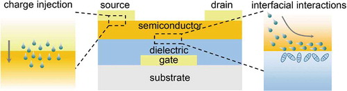
Furthermore, in OFETs, charge transport is also affected by interfaces, which can even mask the intrinsic dependence of mobility on molecular structure and packing. As shown in ), the metal/semiconductor and semiconductor/dielectric interfaces are the places for the charge injection and transport, respectively, which play a fundamental role in the operation of OFETs [Citation5,Citation59–Citation66]. In particular, static structural and energetic disorder encountered by the charges moving along the interface results in percolation motion with certain sites becoming rate limiting for the transport along the interface [Citation67–Citation69]. Due to thermal fluctuations of semiconductor molecules weakly packed by van der Waals (vdW) force at the interface, the disorder might also be dynamic and require charge carriers to remain localized on particular lattice sites until a favourable molecular configuration for charge transfer occurs dynamically [Citation70,Citation71].
Figure 1. (a) Schematic illustration of the OFETs with BGTC configuration. Left panel: charge injection at the metal/semiconductor interface. Right panel: lateral charge transport in the conducting channel at the semiconductor/dielectric interface. (b) Topology micrograph of 30 nm thick C8-BTBT by AFM on (i) SiO2, (ii) PVP, (iii) PMMA, and (iv) CYTOP. A zoomed-in image of the film on CYTOP around defects is given in panel (v), with the phase diagram in panel (vi). Surface contact angle measurements are also shown as insets. (c) Schematic representation of the effect of dielectric-induced charge trapping on contact injection: (i) injection without charge trapping; (ii) injection with significant interface charge trapping. In panel (ii), less + symbols are depicted to represent the reduced mobile carriers at the interface. Fewer arrows represent fewer injected charges, and these arrows are dashed to represent smaller effective carrier mobility. (d) Gate-voltage dependence of the contact resistance for devices with different dielectrics (width normalized). Inset: zoom-in view of data for PMMA and CYTOP. Partially adpated with permission from Ref [Citation74]. .Copyright (2013) American Chemical Society
![Figure 1. (a) Schematic illustration of the OFETs with BGTC configuration. Left panel: charge injection at the metal/semiconductor interface. Right panel: lateral charge transport in the conducting channel at the semiconductor/dielectric interface. (b) Topology micrograph of 30 nm thick C8-BTBT by AFM on (i) SiO2, (ii) PVP, (iii) PMMA, and (iv) CYTOP. A zoomed-in image of the film on CYTOP around defects is given in panel (v), with the phase diagram in panel (vi). Surface contact angle measurements are also shown as insets. (c) Schematic representation of the effect of dielectric-induced charge trapping on contact injection: (i) injection without charge trapping; (ii) injection with significant interface charge trapping. In panel (ii), less + symbols are depicted to represent the reduced mobile carriers at the interface. Fewer arrows represent fewer injected charges, and these arrows are dashed to represent smaller effective carrier mobility. (d) Gate-voltage dependence of the contact resistance for devices with different dielectrics (width normalized). Inset: zoom-in view of data for PMMA and CYTOP. Partially adpated with permission from Ref [Citation74]. .Copyright (2013) American Chemical Society](/cms/asset/6a29ec00-a8e6-488b-a131-c4d36e7275ca/tapx_a_1747945_f0001_oc.jpg)
Based on the position of electrodes with respect to the organic semiconductor layer, four typical device configurations, namely, bottom-gate top-contact (BGTC), bottom-gate bottom-contact (BGBC), top-gate bottom-contact (TGBC), and top-gate top-contact (TGTC), exist [Citation72]. With abundant theoretical and experimental investigations, interfaces are considered as the critical parts in all these device configurations and receive much attention, such as structural defects within the organic layer at the interface, the surface topology and polarity of the dielectric, and the chemical structure of the gate dielectric surface. Also, contact resistance at the source and drain metal/semiconductor interfaces plays an important role, which becomes increasingly important when the length of the channel is reduced and the transistor operates at low fields [Citation61,Citation73]. Moreover, the semiconductor/dielectric interface also has a great effect on the charge injection, indicating that the two interfaces are not completely independent. Liu et al. investigated the influence of gate dielectric interfaces on the contact resistance by using the same organic semiconductor and BGTC device geometry [Citation74]. A large discrepancy in contact resistance from 10 to 66 kΩ cm is observed on different gate dielectrics (), which influence the morphology of the semiconductor layer, the resident trap densities, and the energetic disorder in the semiconductor caused by the randomly oriented dipole in the gate dielectric. Hence, the semiconductor/dielectric interface deserves further attention when investigating the behaviour of charge carriers in organic semiconductors.
In this section, we will simply introduce the disorder and polaron models which are expected to be operative in many organic materials. With these theories, recent attempts in high-performance OFET devices based on the improvements of the semiconductor/dielectric interface will be given.
2.1. Disorder models
The charge carriers are localized over spatially and energetically distributed transport sites in disordered organic materials, and the charge transport is typically modelled using charge hopping theories. It is simple to describe the charge transport via Monte Carlo (MC) simulations, which have two essential inputs, i.e., the charge hopping rates between localized sites and the density of states (DOS) [Citation75].
2.1.1. Hopping rates and density of states
Two main models of charge hopping rates between the localized sites is generally accepted depending on the strength of the electron-phonon coupling, namely, Miller–Abrahams model and Marcus theory. The Miller–Abrahams hopping rate is acceptable for weak electron-phonon coupling and low temperature [Citation68,Citation76,Citation77]. If the polaronic effect is neglected, the hopping rate for a carrier moving from site i to site j is given by:
where is the phonon vibration frequency,
is the inverse localization radius,
is the inter-site distance,
and
are the energies of the site i and j, respectively,
is the difference in site energies between the site i and j, kB and T are the Boltzmann constant and the absolute temperature, respectively. In systems possessing strong electron-phonon coupling, Marcus theory offers a reasonable description of charge transfer of the materials. Based on the assumption that charges are localized on sites and charge-transfer reactions take place via an inter-site hopping conduction, the charge hopping rate at the non-adiabatic (i.e., the strength of the electronic coupling is weak) and high-temperature approximation can be expressed as [Citation78–Citation81]:
In both the Miller–Abrahams and the Marcus approaches, the thermally activated hopping rates vanish when the temperature approaches absolute zero, which is not consistent with the experiments. In addition, considering the high frequency modes in organic semiconductors from conjugated C–C stretching vibrations, typically, , the high temperature approximation in Marcus hopping rate fails. Hence, the classical treatment of environments in Marcus theory should not be appropriate for organic semiconductor systems. To provide a full picture of the charge transport in organic semiconductors, the quantum nuclear tunnelling effect should be considered [Citation82–Citation85]. The nuclear tunnelling assumes that the charge carriers hopping is by tunnelling in an asymmetrically biased double quantum well and charge transfer is driven by the coupling to classical nuclear vibrations ()) [Citation86]. Considering the charge transfer between two localized sites, the charge transfer rate incorporating the quantum nuclear tunnelling effect can be expressed as follows:
Figure 2. Schematic illustrations of the charge transport in organic semiconductors. (a) Schematic representation of electron transfer in a biased double quantum well. The Marcus hopping path and the nuclear tunnelling are indicated by solid-red and dashed-red arrows, respectively. (b) The Bässler’s Gaussian disorder model with a varying width of the Gaussian function σ. (c) The variable range hopping transport. (d) The multiple trap and release (MTR) model. Partically adapted with permission from Ref [Citation128].Copyright (2017) The Royal Society of Chemistry
![Figure 2. Schematic illustrations of the charge transport in organic semiconductors. (a) Schematic representation of electron transfer in a biased double quantum well. The Marcus hopping path and the nuclear tunnelling are indicated by solid-red and dashed-red arrows, respectively. (b) The Bässler’s Gaussian disorder model with a varying width of the Gaussian function σ. (c) The variable range hopping transport. (d) The multiple trap and release (MTR) model. Partically adapted with permission from Ref [Citation128].Copyright (2017) The Royal Society of Chemistry](/cms/asset/beaf266c-ae44-4839-adc2-456ca43225d2/tapx_a_1747945_f0002_oc.jpg)
where and
are the frequency and the occupation number for the jth vibrational mode, respectively; and
is the corresponding Huang–Rhys factor representing the local electron-phonon coupling. This is a full quantum expression in perturbation theory, which considers all vibrational modes at the quantum-mechanical level. In the strong-coupling (
and high-temperature limits
, and the classical limit), the short-time approximation
is applied, in which case, the equation goes to the classical Marcus hopping rate formula.
The charge carriers move via hopping transitions between localized states, which are randomly distributed in space. The energies of charge carriers on these states in organic materials are usually assumed to be of Gaussian shape [Citation75,Citation87]:
where σ is the energy scale of the distribution. The energy scale for DOS is typically of the order of ~0.1 eV. The energetic disorder mainly originates from the fluctuation in the lattice site energies and the distribution of segment length in the π- or σ-bonded main-chain polymer [Citation57]. In particular, the random dipoles present at the semiconductor/dielectric interface in OFET devices could modulate energies of localized states, leading to increased energetic disorder, which is usually reflected in a significant drop in the hole mobility and unsatisfactory device performance ()). According to this mechanism, the efficient way to improve the charge mobility in OFETs is to narrow energy scale of the distribution and reduce the energetic disorder. In recent research, Sun et al. demonstrated an effective buffering method applying an ultrathin PMMA buffering layer between the ferroelectric dielectric and semiconductor layer for high-performance devices () [Citation88]. A high mobility of up to 4.6 cm2 V–1 s–1 was obtained. Based on such high mobility, the programming process in the Fe-OFETs was mainly dominated by switching between two P(VDF-TrFE) polarizations. This enhanced performance was attributed to suppression of the polarization fluctuation at the semiconductor/dielectric interface, efficiently improving the charge transport in conducting channels (). Moreover, with the buffering effect at the semiconductor/ferroelectric interface, the contact resistance was significantly reduced from 260 kΩ cm to 55 kΩ cm, due to the narrowed trap distribution of the organic semiconductor in the contact region () [Citation89].
Figure 3. (a) Schematic illustration of the dipolar disorder at the interface. Partically adapted with permission from Ref [Citation129].Copyright (2004) American Chemical Society. (b) Schematic illustration of a bottom-gate top-contact Fe-OFET with an ultrathin PMMA buffering layer. The polarization fluctuation is well suppressed and the charge carrier transport is enhanced. (c) AFM images of surfaces in the OFET device. Partically adapted with permission from Ref [Citation88].Copyright (2015) Springer Nature Limited. (d) Linear fittings between the value of the RcW – (Vg−Vth) of devices without and with PMMA buffering layer. The inset shows the orientations of the applied electric field and dipole moments in the ferroelectric layer. (e) Schematic of the effect of the polarization fluctuation at the C8-BTBT/P(VDF-TrFE) interface on the contact resistance. (f) Trapped carrier distribution at the access region in devices without and with the PMMA buffering layer. Partically adapted with permission from Ref [Citation89].Copyright (2015) AIP Publishing LLC
![Figure 3. (a) Schematic illustration of the dipolar disorder at the interface. Partically adapted with permission from Ref [Citation129].Copyright (2004) American Chemical Society. (b) Schematic illustration of a bottom-gate top-contact Fe-OFET with an ultrathin PMMA buffering layer. The polarization fluctuation is well suppressed and the charge carrier transport is enhanced. (c) AFM images of surfaces in the OFET device. Partically adapted with permission from Ref [Citation88].Copyright (2015) Springer Nature Limited. (d) Linear fittings between the value of the RcW – (Vg−Vth) of devices without and with PMMA buffering layer. The inset shows the orientations of the applied electric field and dipole moments in the ferroelectric layer. (e) Schematic of the effect of the polarization fluctuation at the C8-BTBT/P(VDF-TrFE) interface on the contact resistance. (f) Trapped carrier distribution at the access region in devices without and with the PMMA buffering layer. Partically adapted with permission from Ref [Citation89].Copyright (2015) AIP Publishing LLC](/cms/asset/0d49fcc3-958c-46be-ad39-c70551e1a9dd/tapx_a_1747945_f0003_oc.jpg)
2.1.2. Gaussian disorder model
Bässler’s Gaussian disorder model (GDM) assumes a disorder-broadened Gaussian density of transport states, and the site positions and energies are considered as independent from each other () [Citation75,Citation90]. At the zero-field limit, the mobility obeys the temperature dependence:
While not involved in the temperature dependence, the dependence of µ on the strength of electric field (F) in the GDM was given in the form [Citation57,Citation75,Citation90]:
where Σ is the standard deviation associated with the off-diagonal disorder, and c is a numerical constant. Note that, the site energies are distributed independently, with no correlations occurring over any length scale. Consequently, the field dependence of the GDM applies only over a very narrow range at high fields () [Citation91]. Novikov et al. presented the correlated Gaussian disorder model (CDM) in which the spatial correlations due to charge-dipole interactions are considered [Citation92]. And the expression for the electric field and temperature dependence of the mobility can be expressed as:
where a is the cell spacing.
2.1.3. Variable-range hopping
Because the hopping rates given by Miller–Abrahams and Marcus approaches depend on the inter-site distances and site energies, the hopping conduction is generally a variable-range hopping (VRH) process () [Citation87]. At low temperatures, the carriers mostly tunnel to spatially remote sites to optimize the activation in energy. While at sufficiently high temperatures, the VRH turns into the nearest-neighbour hopping (NNH), in which charge carriers mostly tunnel to the spatially nearest sites. Variable range hopping assumes that hopping transport takes place via tunnelling among localized states and the probability of each hop depends on the site energy and the hopping distance [Citation93,Citation94]. It has a characteristic temperature dependence of:
where the coefficient varies from different models. The Mott variable range hopping model describes low-temperature conduction in strongly disordered systems with localized charge carrier states, following the temperature dependence [Citation95]:
The Efros–Shklovskii variable-range hopping model accounts for the Coulomb gap in the density of states near the Fermi level due to the interactions between localized charges [Citation96]. The consideration of the Coulomb gap obeys the temperature dependence:
2.1.4. Multiple trapping and release
In polycrystalline films with regular molecular arrangement, the delocalized orbitals of neighbouring molecules partially overlap. Hence, the intermolecular charge-carrier transfer is much more efficient, resulting in a significant larger carrier mobility than that in amorphous films. The MTR theory assumes that the charge carrier transport occurs in a narrow-delocalized band associated with localized levels acting as traps, which locate in a tail of the DOS extending into the highest occupied and lowest unoccupied molecular orbitals (HOMO-LUMO) gap (). From the HOMO (LUMO) edge by a few thermal energies (kBT), the trap states act as deep trap that cannot be thermally activated. For the trap sates within a few thermal energies form the mobility edge, it acts as the shallow traps, which can get excited to a delocalized state through thermal energy, and then the carriers were trapped again until a new thermal release event. In other words, the charge carriers interact with the localized levels through a succession [Citation51,Citation75]. And the mobility relating to the mobility in the delocalized band can be expressed as
where Et is the trapping energy and α represents the ratio between the density of delocalized levels available for transport and the density of traps. In OFETs, not all the charges induced by the gate field contribute to the current flow, for some of the mobile charges can be momentarily trapped by shallow traps; the number of these charges depends on the density of shallow traps and temperature. It suggests that the charge mobility described by MTR model is gate-voltage dependent and thermally activated.
2.2. Polaron-correlated charge transport in OFETs
In this part, we will focus on molecular semiconductors, which are structurally well-defined materials with a very low concentration of defects. Their electronic and vibrational structure is very well known, offering ideal conditions to test theoretical models of transport and to attempt the construction of a relationship between structure and property. A brief introduction of the classical small polaron theory and recent attempts to describe the transport of molecular materials in OFETs will be given.
2.2.1 Classical small polaron models
In the band theory [Citation97], neglecting multielectron effects and interaction between charge carriers, the charge carrier has a delocalized wavefunction with a well-defined momentum, which is scattered by impurities into a state with a different momentum. The frequency of the scattering events increases with increasing temperature. Thus, the mobility decreases with increasing temperature, which is normally the hallmark of the band-like transport, a macroscopic behaviour. Furthermore, when we consider the role of nuclear motions and local electron-phonon coupling, the polaronic band model was proposed. In the low temperature limit, the charge carrier wavefunction remains delocalized (assuming there are no defects). With only a small fraction of charge on each molecule, the deformation of the molecules is small. The charge carrier propagating through the lattice, carrying with the deformation of the surrounding molecules, is called polaron. Since the polaron is delocalized and the system has translational symmetry, the polaron states are expected to be described by a band, whose propagation is similar to a single carrier. Nevertheless, infinite effective mass of the polaron can be achieved at high temperatures, which means that all polaronic states are degenerate. Thus, it is more convenient to describe the carrier wavefunction as localized on a single molecule. The polaron moves from site to site, whose dynamics can be described in a model containing only two sites. For historical reasons, this small polaron theory is more often described in the diabatic limit [Citation98–Citation101]. At high temperatures, the hopping rate is identical to the expression of charge transfer rate obtained by popular Marcus theory due to its simplicity [Citation76]. If a small polaron is formed, the transport is thermally activated, i.e., the mobility increases with increasing temperature unlike in the polaronic band model.
2.2.2 Polarons at semiconductor/dielectric interface in OFETs
Under the framework of the small polaron models, most theories consider the possibility that charge carriers behave as Holstein polarons [Citation102], a more realistic lattice model for polarons, whose spatial extent can be either short-range within few atoms or long-range over several atoms. Nevertheless, in OFET devices, the charge carriers move at the interface with a polar dielectric, whose properties should be key factors [Citation103]. The polaron behaviour near surfaces is significantly different from that in bulk crystals. Specifically, the rough surface morphology will largely change in the effective potential and introduce anisotropy in the effective mass of polaron. In such a situation, there will be changes in the surface-polaron energy, cyclotron-resonance frequency, and localizations parallel to the surface. Moreover, the electrical property of the gate-dielectric is another critical factor. The dielectric constant determines the interface disorder and electrostatic interactions to a large extent, which will also have a great influence on the charge transport behaviours at the semiconductor/dielectric interface, strongly correlated with Fröhlich polarons [Citation28,Citation104–Citation106]. Thus, the dielectric/organic interfaces can provide an ideal model system for the controlled study of Fröhlich polarons with tunable coupling.
Hulea et al. and his coworkers have studied temperature-dependent electrical transport through organic single-crystal FETs using six different gate insulators [Citation107]. The dielectric constant (ε) of the gate insulator is varied from 1 to 25. Measurements were carried out between 300 and 200 K to avoid the formation of cracks in the crystals because the difference between the thermal expansion of the organic material and their supporting substrates often causes device failure. Notably, it has been observed that the temperature dependence of the mobility evolves from metallic-like (dμ/dT < 0) to insulating-like (dμ/dT > 0) as ε increases. Moreover, the dependence of the threshold charge on temperature and ε has also been investigated. Contrary to the threshold voltage shift, the shift of the threshold charge with temperature does not depend on the thickness of the gate insulator but only the dielectric/organic interface. Hence, the effect of the ε of the gate insulator on the mobility of charge carriers is an intrinsic property of dielectric/organic interfaces, which suggests that the observed phenomenon originates from the interaction of the charge carriers with their polar environment. This interaction can be quantitatively described by a two-dimensional Fröhlich polaron model, in which free electrons interact with a dispersionless optical phonon of characteristic frequency ωs. The use of gate dielectrics with increasing ionic polarizabilities permits the strength of the interaction to be tuned from the weak to the strong coupling regime.
In addition, abundant theoretical calculations on polaronic effects have been done by Kirova et al. and his coworkers [Citation59]. For typical parameters of molecular field-effect transistors, the binding energy is found to be high enough to allow for the formation of a strongly coupled polaron. Such surface polaron will behave as the enhanced effective mass, midgap states, and pseudogap regime in the case of tunnelling experiments, which will be more stable in the presence of a bias electric field.
2.2.3 Dynamic disorder
In fact, developments in the fundamental understanding of the charge transport in ordered organic materials have been well beyond the semiclassical band theory frameworks with more and more experimental support. Particularly, one of the important progresses is dynamic disorder [Citation108–Citation111], which is due to the intermolecular vibrations or fluctuations. Plenty of experiments reported that there is a region where band-like tunnelling works (dµ/dT < 0), which is contrast to the traditional understanding of the incoherent hopping transport in localized polarons. This abnormal phenomenon in ordered organic materials originates from the very weak interactions among the molecules. The dynamic disorder causes a transient localization over a length Lτ within a fluctuation time τos, which is the inverse of the typical intermolecular oscillation frequency. Then, the intrinsic mobility in the crystal can be written as , exhibiting the band-like dependence of the charge mobility. In addition, this model is consistent with the spectroscopic observation of localized carriers. Ando et al. and his coworkers characterized the electrical properties of OFET devices with zonecast pentacene films. They used the in situ micro-Raman spectroscopy, which could both probe the dynamic and static disorder, to monitor the intermolecular and the intramolecular vibrational peaks of films [Citation112]. Under gate-bias stress, photoexcitation, and thermal annealing, transformations from a high-temperature (HT) phase with reduced molecular vibration along the long axis and transformations from a low-temperature (LT) with increased molecular vibration that were induced by the electron delocalization were observed. The changes were induced by electron localization (HT) and delocalization (LT) in pentacene molecules at the channel interface. In addition, multilayer molecular dynamics simulations were also carried out, revealing that electrons should be localized in each pentacene molecule to make the low-temperature phase more stable by freezing the vertical molecular disorder. A unified picture was proposed to describe the relationship between structural disorder and localization dynamics in pentacene polymorphs (), reflecting the competition between vdW force, thermal vibration, and electronic Coulomb repulsive force under interaction with the substrate surface.
Figure 4. The cross-sectional pentacene molecule arrangements on a dielectric surface, showing the structure-property relationship in pentacene polymorphs. Partically adapted with permission from Ref [Citation112].Copyright (2019) American Physical Society
![Figure 4. The cross-sectional pentacene molecule arrangements on a dielectric surface, showing the structure-property relationship in pentacene polymorphs. Partically adapted with permission from Ref [Citation112].Copyright (2019) American Physical Society](/cms/asset/3d8ce493-a467-41ad-a53b-03fc001a3bda/tapx_a_1747945_f0004_oc.jpg)
In the researches, numerous technologies are introduced to characterizing the interfaces, such as in-situ low-temperature scanning tunnelling microscopy, synchrotron-based high-resolution ultraviolet photoelectron spectroscopy, near-edge X-ray absorption fine structure measurements, and scanning Kelvin probe microscopy (SKPM). Nevertheless, these indirect examinations on interfaces only give us partial evidences. Especially in bulk films, the channel defects in bulk semiconductors scatter charges and hinder current flow. Thus, it is difficult for carriers to maintain their original behaviour under the influence of the dielectric layers, which can mislead researchers about the nature of the semiconductor/dielectric interface in such indirect measurements.
To get a more accurate understanding of the interfaces, a very promising solution is the interface-like films. Marta Tello et al. tried to decrease the thickness of pentacene film to ~7 nm, but high-quality film was not achieved. When the thickness was reduced, the holes and grain boundaries were observed in the surface topography [Citation26](). Moreover, the mobilities were found to be lower by about one order of magnitude than the devices using thick films of pentacene. In SKPM measurements, the potential data observed on the thin films exhibited a one-to-one correlation between potential distributions of the trapped charge and the surface topography (). Most of the applied drain-source bias drops across a single well-defined grain boundary. The morphological defects and misalignment of crystalline grains can completely obscure the intrinsic charge transport properties of materials, resulting in the largely degraded device performance (). Thus, efforts should be devoted to improving and exploring novel deposition techniques for high-quality semiconducting films.
Figure 5. (a) (i)Topographic area scan of the 30-nm-thick pentacene film taken on the channel (the electrodes lie at both sides of the channel); (ii) topography of the 20-nm-thick film; (iii) and (iv) topography for the 7-nm-thick film. (b) Potential maps at the pentacene/HMDS interface of a masked sample taken at different gate voltages. (i) Vgs = 0 V, (ii) Vgs = −10 V. (c) (i) The cross-section image of the transistor, with the thicker regions (pentacene grains) and the thinner regions (IGRs); (ii) Top view of the encircled area in (i): ① crystalline grains; ② relatively ordered pentacene clusters; ③ regions with no or incomplete pentacene coverage and poor connectivity. Partically adapted with permission from Ref [Citation26].Copyright (2008) WILEY-VCH Verlag GmbH & Co. KGaA, Weinheim
![Figure 5. (a) (i)Topographic area scan of the 30-nm-thick pentacene film taken on the channel (the electrodes lie at both sides of the channel); (ii) topography of the 20-nm-thick film; (iii) and (iv) topography for the 7-nm-thick film. (b) Potential maps at the pentacene/HMDS interface of a masked sample taken at different gate voltages. (i) Vgs = 0 V, (ii) Vgs = −10 V. (c) (i) The cross-section image of the transistor, with the thicker regions (pentacene grains) and the thinner regions (IGRs); (ii) Top view of the encircled area in (i): ① crystalline grains; ② relatively ordered pentacene clusters; ③ regions with no or incomplete pentacene coverage and poor connectivity. Partically adapted with permission from Ref [Citation26].Copyright (2008) WILEY-VCH Verlag GmbH & Co. KGaA, Weinheim](/cms/asset/edab630f-3ea3-4f34-963c-4405b28256f9/tapx_a_1747945_f0005_oc.jpg)
3 Examinations and explorations of interfacial effects using 2DMCs
In recent research, various techniques have been extensively used to achieve high-quality 2D organic crystalline films, such as floating-coffee-ring assembly [Citation38], solution shearing [Citation113], dip-coating [Citation114,Citation115], drop-casting [Citation116], antisolvent-assisted spin coating [Citation63] and solution epitaxy [Citation43,Citation117]. The superior interface qualities of the highly uniform 2DMCs with long-range molecular ordering can be promising materials to overcome the obstacles in traditional organic thin films, excluding the effects of extrinsic factors [Citation5,Citation41,Citation118,Citation119]. Therefore, the 2DMCs can provide great possibilities to directly explore the intrinsic nature of the charge carrier behaviours at the semiconductor/dielectric interface.
3.1 Modulations of interactions at semiconductor/dielectric interfaces
The crystalline structure and the properties can be easily tuned due to the weak vdW forces in organic semiconductors, especially at the 2D limit. When the dimension decreases from bulk to monolayer or a few molecular layers, the molecule–substrate interaction becomes non-negligible. The three most important interactions, namely, molecule–substrate interaction (Isubstrate), intralayer (Iintralayer), and interlayer (Iinterlayer) vdW interactions between adjacent molecules, are balanced during the growth of the few-layer organic semiconductor films. Iinterlayer that commonly exists in conventional bulk organic crystals can be significantly eliminated in the few-layer geometry. Consequently, the molecular packing in few-layer organic crystals is greatly influenced by the competition between Iintralayer and Isubstrate [Citation120,Citation121]. This condition opens up a new way to precisely control the molecular layers by tuning the interfacial interaction.
Wu et al. demonstrated the epitaxy of organic semiconductors with self-limited characteristics at the precision of molecular layers by exploiting the interfacial vdW forces between graphene and C8-BTBT molecules [Citation122]. A relatively large C8-BTBT molecule–graphene binding energy gradient exists near the interface (). The binding energy is highest on the graphene substrate but rapidly decreases on the interfacial layer (IL) and the subsequent first conducting layer. Thus, the binding energy gradient creates a temperature window, where the adsorbed C8-BTBT molecule is thermodynamically stable on graphene but unstable on IL. Thus, the self-limited epitaxy of monolayer can be realized. The bilayer (interfacial layer and first conducting layer) C8-BTBT can also be realized by simply adjusting the substrate temperature (). Strong Isubstrate dominates the molecular packing in the initial growth. The molecules with weak Iintralayer most likely flat lie to maximize Isubstrate, and thus, the molecules adopt face-on or a largely tilted configuration. As the molecule coverage increases, Iintralayer would become larger than Isubstrate. The adsorbed molecules can then flip up from a parallel to the upright direction to the substrate. They also demonstrated the layer-by-layer epitaxy of ultrathin PTCDA/C8-BTBT heterostructures, and the p–n heterojunction was further exploited for photodetector applications, which are shown in . The photovoltaic responses with an open-circuit voltage of ~0.5 V and photoresponsivity of ~0.37 mA/W were achieved. Thus, the layered small-molecule semiconductors break the limitation of bulk heterojunctions and open new possibilities for optoelectronic devices.
Figure 6. (a) Top panel: schematic illustration of the growth furnace. Bottom panel: temperature inside the furnace as a function of distance to the centre (black symbols, measured; red line, a guide to the eye). (b) Blue dots: calculated binding energies of a single C8-BTBT molecule on graphene, IL/graphene, the first conducting layer/IL/graphene, and the second conducting layer/the first conducting layer/IL/graphene. Red dash line: C8-BTBT−C8-BTBT interaction. Inset shows the molecular structure of C8-BTBT and molecular packing of different C8-BTBT layers on graphene. (c) AFM images of typical samples after C8-BTBT growth in Zone I (i), Zone II (ii), and Zone III (ⅲ), respectively. (d) Output characteristics of the p-n junction under the linear scale (black) and log scale (blue). Inset is schematic layout of the PTCDA/C8-BTBT p-n heterojunction device. (e) Output characteristics of the p-n junction under the dark conditions (black) and the 0.67 μW laser illumination (red). Partically adapted with permission from Ref [Citation122].Copyright (2016) American Chemical Society. (f) Schematic of the growth from polycrystalline films to bilayer and monolayer C8-BTBT films. (g) Work of adhesive between the first conducting C8-BTBT layer and SiO2 and between the frist and second conducting layers in C8-BTBT. The red dot line is the work of adhesive between the C8-BTBT and C8-BTBT. The inset is the molecular packing schematic of bilayer and monolayer films. (h) Assembled length of monolayer (blue square dots) and bilayer (red circle dots) C8-BTBT films as a function of the substrate temperature (T). Partically adapted with permission from Ref [Citation124].Copyright (2018) American Chemical Society
![Figure 6. (a) Top panel: schematic illustration of the growth furnace. Bottom panel: temperature inside the furnace as a function of distance to the centre (black symbols, measured; red line, a guide to the eye). (b) Blue dots: calculated binding energies of a single C8-BTBT molecule on graphene, IL/graphene, the first conducting layer/IL/graphene, and the second conducting layer/the first conducting layer/IL/graphene. Red dash line: C8-BTBT−C8-BTBT interaction. Inset shows the molecular structure of C8-BTBT and molecular packing of different C8-BTBT layers on graphene. (c) AFM images of typical samples after C8-BTBT growth in Zone I (i), Zone II (ii), and Zone III (ⅲ), respectively. (d) Output characteristics of the p-n junction under the linear scale (black) and log scale (blue). Inset is schematic layout of the PTCDA/C8-BTBT p-n heterojunction device. (e) Output characteristics of the p-n junction under the dark conditions (black) and the 0.67 μW laser illumination (red). Partically adapted with permission from Ref [Citation122].Copyright (2016) American Chemical Society. (f) Schematic of the growth from polycrystalline films to bilayer and monolayer C8-BTBT films. (g) Work of adhesive between the first conducting C8-BTBT layer and SiO2 and between the frist and second conducting layers in C8-BTBT. The red dot line is the work of adhesive between the C8-BTBT and C8-BTBT. The inset is the molecular packing schematic of bilayer and monolayer films. (h) Assembled length of monolayer (blue square dots) and bilayer (red circle dots) C8-BTBT films as a function of the substrate temperature (T). Partically adapted with permission from Ref [Citation124].Copyright (2018) American Chemical Society](/cms/asset/06548dc6-4ac2-4b34-82a0-60af23fd4775/tapx_a_1747945_f0006_oc.jpg)
Recently, Jiang et al. reported the thermally induced self-assembly of few-layer organic crystalline films with a well-defined molecular layer number over a millimetre-sized area via interfacial-interaction modulation [Citation124]. The C8-BTBT solution was drop-cast on the SiO2/Si substrate. Then, the polycrystalline films were obtained after the solvent evaporated. Note that the solution-processed C8-BTBT crystalline films is different from those deposited by physical vapor transport method, the first layer is also a conducting layer instead of an interfacial layer. The interaction between the monolayer C8-BTBT and the SiO2/Si substrate is the strongest. It decreases between the bilayer and monolayer C8-BTBT, which is slightly larger than that of C8-BTBT–C8-BTBT in the upper layers (). The gradient interaction indicates that the upper-layer molecules are more thermodynamically unstable than the molecules in the first two monolayers. Hence, a defined temperature window exists, in which the polycrystalline films can be controlled to molecular bilayer or monolayer films (). The strong molecule–substrate interactions dominate the interfacial molecular packing by increasing the substrate temperature, leading to large-area irregular monolayer molecular films.
Besides, under the effective modulations of interactions at semiconductor/dielectric interfaces, the prominent features combined with the unique merits of material versatility and ease of processing allow OFETs suitable for various potential functional applications, such as photoelectric detection, biosensing, and data storage. Pei et al. scaled down the organic functional layers to a 2D limit with good uniformity over a large area [Citation123]. The quasi-2D ferroelectric dielectric layers are beneficial for low-voltage operations. Moreover, the few-layered C8-BTBT can significantly enhance the charge injection, speeding up the data switching that corresponds to rapid the carrier accumulation and depletion at the semiconductor/dielectric interface. Thus, pJ-level energy consumption is obtained, which is < 0.1% of the energy required for devices using bulk functional layers, opening up a path towards emerging applications, such as wearable electronics.
3.2 Structure-related charge transport properties
The highly clean system allows us to directly investigate carrier transport and structure-property relationship at the interface without being dominated by extrinsic factors. Zhang et al. achieved highly ordered single-crystalline mono- to tetralayer pentacene crystals on hexagonal BN substrates through the vapour transport method [Citation125]. With atomic force microscopy (AFM) and transmission electron microscopy (TEM) characterizations, the molecular packing of the interfacial layer considerably differs from that of the subsequent layers. The average thickness of the IL is 0.5 nm, indicating that the molecules adopt the face-on configuration. The second conducting layer is 1.58 nm, which is consistent with the thin-film phase of pentacene. Unlike the normal polymorph, the first conducting layer is 1.14 nm. The latter is a new polymorph, which shows a reduced height compared with the second conducting layer, thereby suggesting a more tilted molecular packing. High-resolution AFM measurements were performed to gain further structural information of the pentacene layers. With the direct characterizations of each layer, the unit cell expanded significantly by 0.2 Å (or 3.3%) along the a-axis, whereas minimal expansion was observed along the b-axis. In addition, differences were observed along the a-axis when comparing the bulk and thin-film phases of pentacene.
Based on the quantitative structural characterization, they investigated the thickness-dependent electrical transport in pentacene crystals using backgated OFET geometry. Inferred by temperature-dependent electrical measurements, the charge transport is dominated by hopping in the first conducting layer. By adopting the fitting procedure, the Urbach energy in localized states is much smaller than that in disordered 2D organic semiconductors, which is comparable with the best value for conjugated polymers. Besides, the localization length ~1 nm is a natural result of the molecular packing in the first layer. Surprisingly, the band-like transport was observed in subsequent layers. The difference in mobility became dramatic at low temperature as the mobility of the second layer in devices improved with decreasing T, consistent with band-like transport and lack of localization (). The structural modulation becomes negligible beyond the second conducting layer, leading to a mobility saturation thickness of only ~3 nm, which should be a generic attribute of high-quality layered organic semiconductors. Therefore, the layer-defined highly ordered organic ultrathin films provide a platform for new physics and device structures that are impossible in conventional bulk crystals.
Figure 7. (a) Ids−Vg characteristics at different temperatures of the same device under Vds = −2 V (symbols), plotted on a double logarithmic scale. From top to bottom, T = 300, 250, and 140 K, respectively. The lines are power-law fitting results. Inset shows the extracted power exponent as a function of 1000/T (symbols). The linear fitting crosses the origin (line), consistent with the 2D hopping mechanism. T0 = 331 K is derived from the linear fitting. (b) Experimental (symbols) and calculated (lines) mobility as a function of 1000/T under Vg = −30 (purple), −20 (blue), and −10 V (orange). The calculations are done with the following parameters: T0 = 331 K, σ0 = 1.3 × 10⁶ S/m, α−1 = 8.2 Å. (c) The extracted mobility as a function of Vg at the same temperatures. (d) Mobility as a function of temperature under Vg = −20 (orange), −35 (blue), and −50 V (purple). (e) Side views of the molecular orbitals of the intermolecular bonding states for first (blue) and second (red) conducting layers in the b-c plane, illustrated by isosurface contours of 0.000 15 e/Bohr [Citation3]; Partically adapted with permission from Ref [Citation125].Copyright (2016) American Physical Society
![Figure 7. (a) Ids−Vg characteristics at different temperatures of the same device under Vds = −2 V (symbols), plotted on a double logarithmic scale. From top to bottom, T = 300, 250, and 140 K, respectively. The lines are power-law fitting results. Inset shows the extracted power exponent as a function of 1000/T (symbols). The linear fitting crosses the origin (line), consistent with the 2D hopping mechanism. T0 = 331 K is derived from the linear fitting. (b) Experimental (symbols) and calculated (lines) mobility as a function of 1000/T under Vg = −30 (purple), −20 (blue), and −10 V (orange). The calculations are done with the following parameters: T0 = 331 K, σ0 = 1.3 × 10⁶ S/m, α−1 = 8.2 Å. (c) The extracted mobility as a function of Vg at the same temperatures. (d) Mobility as a function of temperature under Vg = −20 (orange), −35 (blue), and −50 V (purple). (e) Side views of the molecular orbitals of the intermolecular bonding states for first (blue) and second (red) conducting layers in the b-c plane, illustrated by isosurface contours of 0.000 15 e/Bohr [Citation3]; Partically adapted with permission from Ref [Citation125].Copyright (2016) American Physical Society](/cms/asset/91d16e37-8e76-497d-ac78-6275c2e6bf23/tapx_a_1747945_f0007_oc.jpg)
Similarly, based on the layer-defined highly crystalline molecular C8-BTBT fabrication technique, He et al. investigated the intrinsic mobility and contact properties of crystalline monolayer OFETs [Citation126]. In conventional solution-processed or vacuum-deposited OFETs, the thickness of the organic film has to reach a certain value for efficient charge transport due to interfacial defects and traps. An ultimate monolayer of C8-BTBT molecules was used as an OFET channel and demonstrated remarkable electrical characteristics, including intrinsic hole mobility over 30 cm2 V−1 s−1, ohmic contact with resistance of 100 Ω cm, and band-like transport down to 150 K. Compared with conventional OFETs, the main advantage of a monolayer channel is the direct, nondisruptive contact between the charge transport layer and metal electrodes, which is a feature vital for achieving low contact resistance and current saturation voltage. By contrast, bilayer and thicker C8-BTBT OFETs exhibited strong Schottky contact and much higher contact resistance, which were confirmed by the thickness-dependent measurements. The bilayer and trilayer devices showed strong nonlinearity at low Vds regime, in clear contrast with monolayer devices (). The low-bias resistance in bilayer and trilayer devices was completely dominated by contacts, which was approximately two and four orders of magnitude higher than that of the monolayer device, respectively. The Schottky contact was further confirmed by the thermally activated behaviour at low temperature (). Below the flat-band voltage, the Schottky barrier ΦB had a linear dependence on Vg, because thermionic emission was dominant. At the flat-band voltage, thermally assisted tunnelling became relevant, and ΦB started to deviate from the linear trend. Such exponentially large contact resistance with strong nonlinear current-voltage characteristics in the bilayer and thicker devices is due to the increased Schottky barrier width that suppresses tunnelling. Density functional theory calculations were also performed to study the contact and transport properties. The results demonstrated the potential of crystalline monolayer organic semiconductors as building blocks for high-performance and low-power-consumption OFETs and as clean systems for studying device physics.
Figure 8. (a) Schematic illustration of the contact between Au and C8-BTBT. The right part is overlaid by the charge density in the energy range of [EF−0.5 eV, EF]. EF is the Fermi energy of the system. The distribution of charge density along the z direction is plotted. (b) Room temperature double-sweep Ids-Vg characteristics (black line) and the extracted four-terminal field-effect mobility as a function of Vg (red circle). (c) Room temperature Ids-Vds characteristics for typical monolayer, bilayer, and trilayer devices. (d) Arrhenius plot of Ids (Vg = −70 V, Vds = −1 V) of the monolayer (red circle) and bilayer (blue circle) devices in (a). The inset shows energy band diagrams near the contact, with different mechanisms. (e) Arrhenius plot of ln(Ids/T3/2) of the bilayer device in (c). From top to bottom: Vg = −60.4, −56.4, −52.4, −48.4, −44.4, and −40.4 V. (f) Derived Schottky barrier height as a function of Vg. The true Schottky barrier height is 140 meV, as pointed by the arrow. Partically adapted with permission from Ref [Citation126].Copyright (2016) American Association for the Advancement of Science
![Figure 8. (a) Schematic illustration of the contact between Au and C8-BTBT. The right part is overlaid by the charge density in the energy range of [EF−0.5 eV, EF]. EF is the Fermi energy of the system. The distribution of charge density along the z direction is plotted. (b) Room temperature double-sweep Ids-Vg characteristics (black line) and the extracted four-terminal field-effect mobility as a function of Vg (red circle). (c) Room temperature Ids-Vds characteristics for typical monolayer, bilayer, and trilayer devices. (d) Arrhenius plot of Ids (Vg = −70 V, Vds = −1 V) of the monolayer (red circle) and bilayer (blue circle) devices in (a). The inset shows energy band diagrams near the contact, with different mechanisms. (e) Arrhenius plot of ln(Ids/T3/2) of the bilayer device in (c). From top to bottom: Vg = −60.4, −56.4, −52.4, −48.4, −44.4, and −40.4 V. (f) Derived Schottky barrier height as a function of Vg. The true Schottky barrier height is 140 meV, as pointed by the arrow. Partically adapted with permission from Ref [Citation126].Copyright (2016) American Association for the Advancement of Science](/cms/asset/b23edf4c-a39f-4f5b-bb9c-d96fbebe9e88/tapx_a_1747945_f0008_oc.jpg)
When the conducting channel downscaled to a 2D limit, the modulation effect induced by the dielectric can be further strongly verified. Wang et al. demonstrated the fabrication of organic FETs based on 2D crystalline films as semiconducting channels [Citation127]. Considering that a low operating voltage is a pursuit that has always been, they used high-κ oxide dielectrics. When AlOx was applied as the dielectric layer, the devices exhibited a high electrical performance with a carrier mobility up to 9.8 cm2 V−1 s−1, indicating that the AlOx layer was beneficial to the charge transport in the conducting channels of FETs. For comparison, they prepared FET samples that utilized SiO2 and HfO2. A large operating voltage of −20 V was necessary to operate the SiO2-based device, with the maximum estimated carrier mobility of 16 cm2 V−1 s−1, which was higher than that using AlOx layers. Charge carriers are more localized and generate the interfacial Fröhlich polarons because the highly polarizable AlOx dielectrics promotes strong charge–dipole coupling. Moreover, the localization of polarons at the interface was more than those in the bulk due to the distance-dependent charge–dipole interaction. Thus, a marked decline of the charge-carrier mobility can be observed when using high-κ dielectrics. When applying HfO2 as the gate insulator, the operating voltage can be properly lowered to −4 V, whereas the carrier mobility can be as low as 0.4 ± 0.3 cm2 V−1 s−1. For further investigation, the maximum density of interfacial traps (Ntrap) was estimated from the values of the subthreshold swing to examine the performance, especially the carrier mobility. In the device that uses AlOx, the value of Ntrap is ~3.9 × 1012 cm−2, which was in the same range as that using SiO2 or HfO2. Then, they performed the temperature-dependent measurement to characterize the charge transport behaviour in the FETs with different oxide dielectrics (). The device using AlOx exhibits the lowest Ea value of 30.8 meV and a high μ0 of 12 cm2 V−1 s−1. Considering that Ea is related to the width of the distribution of trap states, the high carrier mobility obtained in the AlOx-based device is attributed to a low energetic disorder and a narrow width for the density of trap states in the dielectric interface, whereas the decreased mobility in the device with HfO2 is due to the strong interaction at the interface between the 2D conducting channel and high-κ dielectric. This interaction increases the localization of the charge carriers, which is consistent with the result that SiO2-based OFETs exhibit higher carrier mobility than the AlOx-based devices. Therefore, the dielectric layer has a significant influence on the charge transport behaviours in conducting channels.
Figure 9. (a) Transfer curves of the C8-BTBT-based OFETs using AlOx, HfO2 and SiO2 under different temperatures. (b) Temperature dependence of the field-effect mobility. Partically adapted with permission from Ref [Citation127].Copyright (2017) Springer Nature Limited
![Figure 9. (a) Transfer curves of the C8-BTBT-based OFETs using AlOx, HfO2 and SiO2 under different temperatures. (b) Temperature dependence of the field-effect mobility. Partically adapted with permission from Ref [Citation127].Copyright (2017) Springer Nature Limited](/cms/asset/97123fae-a6b7-4924-ae27-c87b35d6c2c5/tapx_a_1747945_f0009_oc.jpg)
The 2DMCs provide high possibilities for the improvement and fictionalization of devices due to the direct modulation of the interface between conducting channel and dielectric layer. Therefore, highly ordered organic ultrathin films offer a platform for new physics and device structures that are impossible in conventional bulk crystals. Being atomically thin, they provide unprecedented access to the exploration of fundamental interface science at the nanoscale, which is essential for device miniaturization development.
3.3 Interfacial templating effect
Considering the large area uniformity and continuity of the highly ordered 2DMCs, they can act as the molecular templating layer to induce the upper layer molecules to form high-quality thin films with controllable properties, such as molecular orientation, film morphology, and electronic structure. Wang et al. reported a highly ordered organic monolayer with large-area uniformity acting as the templating layer between the dielectric and thermally evaporated semiconducting layers [Citation63]. Anisole solution of C8-BTBT and immiscible N,N-dimethylformamide (DMF) were sequentially dropped onto a phenyltrichlorosilane-treated hydrophilic SiO2/Si substrate for spin-coating process. In the process, DMF spread rapidly over the anisole surface, while the assembled molecules spontaneously aggregated into the floating crystalline nanosheets at the anisole/DMF interface. The ultrathin crystalline sheets grew equatorially larger and connected, evolving into large-area, continuous monolayer crystals, with substrate coverage that reached up to ~97% at the optimal spin speed and solution concentration. The monolayer molecular crystals exhibited very small surface roughness of ~1.93 Å. TEM and its corresponding SAED indicated a highly ordered molecular packing (). Subsequently, the as-prepared monolayer molecular crystals with large-area uniformity and high crystallinity acted as an interfacial templating layer for the growth of 27 nm-thick upper films via the thermal evaporation (). The hybrid-deposited films exhibited almost single crystalline, meaning that the interfacial monolayer crystals exhibited a strong templating effect to guide the packing behaviour of the upper layer molecules (). The mobility of the hybrid-deposited films was as high as 11.3 cm2 V−1 s−1, which is higher than that without this templating monolayer by nearly one order of magnitude. Such significantly enhanced electrical performance was ascribed to the enhanced crystallinity and highly organized arrangement of the upper evaporated films induced by bottom spin-coated monolayer crystals. Transistor arrays based on the hybrid-deposited films exhibited an average mobility of 7.7 cm2 V−1 s−1 with high uniformity, which can be compatible with patterning technology.
Figure 10. (a) Structure of a bottom-gate top-contact transistor with a spin-coated C8-BTBT monolayer at the semiconductor/dielectric interface and the molecular structure of C8-BTBT. (b) Optical microscopy of deposited C8-BTBT. (c) SAED patterns of the C8-BTBT monolayer. (d) XRD patterns of the C8-BTBT films with total thicknesses of (i) 6 nm and (ii) 30 nm without and with spin-coated monolayers at different speeds. (iii) The d-spacing (blue) and fwhm (olive) data calculated from the 6 nm thick (squares) and 30 nm thick (circles) films. The films on the reference samples were deposited by thermal evaporation. Partically adapted with permission from Ref [Citation63].Copyright (2018) American Chemical Society. (e) Optical microscopy image of a PTCDI-C8/C8-BTBT heterojunction. PTCDI-C8 grown on the SiO2 and monolayer C8-BTBT film. (f) AFM image of PTCDI-C8 grown on the SiO2 and monolayer C8-BTBT films. The height profile shows the PTCDI-C8 is the molecular monolayer. (g) Transfer characteristics of transistors with monolayer PTCDI-C8 on monolayer C8-BTBT template (red line) and the SiO2 substrate (blue line). The inset is the schematic illustration of the heterojunction device. Partically adapted with permission from Ref [Citation124].Copyright (2018) American Chemical Society
![Figure 10. (a) Structure of a bottom-gate top-contact transistor with a spin-coated C8-BTBT monolayer at the semiconductor/dielectric interface and the molecular structure of C8-BTBT. (b) Optical microscopy of deposited C8-BTBT. (c) SAED patterns of the C8-BTBT monolayer. (d) XRD patterns of the C8-BTBT films with total thicknesses of (i) 6 nm and (ii) 30 nm without and with spin-coated monolayers at different speeds. (iii) The d-spacing (blue) and fwhm (olive) data calculated from the 6 nm thick (squares) and 30 nm thick (circles) films. The films on the reference samples were deposited by thermal evaporation. Partically adapted with permission from Ref [Citation63].Copyright (2018) American Chemical Society. (e) Optical microscopy image of a PTCDI-C8/C8-BTBT heterojunction. PTCDI-C8 grown on the SiO2 and monolayer C8-BTBT film. (f) AFM image of PTCDI-C8 grown on the SiO2 and monolayer C8-BTBT films. The height profile shows the PTCDI-C8 is the molecular monolayer. (g) Transfer characteristics of transistors with monolayer PTCDI-C8 on monolayer C8-BTBT template (red line) and the SiO2 substrate (blue line). The inset is the schematic illustration of the heterojunction device. Partically adapted with permission from Ref [Citation124].Copyright (2018) American Chemical Society](/cms/asset/7c01f50e-67ed-4c09-afb1-53c731178641/tapx_a_1747945_f0010_oc.jpg)
Large-area monolayer C8-BTBT with high uniformity was also employed as an interfacial templating layer to construct a vertical PTCDI-C8/C8-BTBT heterojunction by Jiang et al [Citation124]. They found that a continuous PTCDI-C8 film on monolayer C8-BTBT with high uniformity was formed, whereas numerous small isolated islands were formed on SiO2/Si substrate and monolayer C8-BTBT films with polyporous structure, indicating the efficient interfacial templating effect (). The ambipolar OFETs based on the heterojunctions exhibited balanced electron and hole mobilities of 0.6 and 0.4 cm2 V−1 s−1, respectively (). This efficient and feasible method via interfacial-interaction modulation with controllable molecular layers and scale-up coverage enables the achievement of advanced organic electronic applications, such as quantum wells and superlattices.
4 Conclusion and outlook
Organic semiconductors are undergoing an exponential development due to their extraordinary electrical, chemical, thermal, and optical properties. When it is used as the conducting channel in OFETs for various functional applications, the device performance is closely related to the charge transport properties in conducting channels, which largely depend on the semiconductor/dielectric interface. Hence, elucidating the nature of charge carriers at the semiconductor/dielectric interface is of great importance for clarifying the structure-property relationships and achieving high-performance OFET devices for sustainable advancement in organic electronics. To have an overall observation of the interfacial properties, numerous optical and electrical technologies are applied, such as in-situ low-temperature scanning tunnelling microscopy, near-edge X-ray absorption fine structure measurements, and scanning Kelvin probe microscopy. The motion of charge carriers has been extensively explored with various transport models based on bulk organic crystals. Note that traditional 3D bulk films often have complex microstructures and undesirable qualities, study on interfaces suffers from indirect examinations, which only gives us partial evidences. To have a more accurate and in-depth understanding of the intrinsic semiconductor/dielectric interface properties, high-quality interface-like films are urgently needed for direct characterizations, eliminating these undesirable qualities. Recently, the emerging 2D organic crystals can be a good choice. The unique characteristics of atomically flat surface and long-range molecular ordering realize the minimization of excessive disorders and traps in crystals. Moreover, under the 2D geometry, the interface-like films eliminate the interlayer screening and provide full exposure for more direct exploration of device physics, such as intrinsic charge transport and interfacial effects. Hence, the interface-like film is a powerful platform to explore fundamental device physics and promote the revolutionary advancement in organic electronics.
Although great progress has been achieved through these works, challenges remain in this field. Efforts should be devoted to the further improvement of transport properties by optimizing dielectric materials. The dielectric properties and device performance are commonly related because the surface morphology always has a strong influence on the aggregation of the overlying organic molecules into the crystalline nanosized domains, which can be related to the efficient transport of the charge carriers. Hence, an in-depth understanding of the correlation between nanoscale morphology at the semiconductor/dielectric interface and charge transport properties is urgently required. In particular, reliable theoretical models and reasonable experimental design can serve as corporate guidance to the modification of the nanoscale morphology of the dielectric layers, thereby developing suitable and easily processable dielectric materials and utilizing their special characteristics (such as piezoelectricity, ferroelectricity, pyroelectricity, and even traps) to realize highly functional smart designs. Quantitative information at the atomistic level provided by numerical simulations is also helpful. 2DMCs combined with high-quality dielectrics should be focused as a clear and powerful platform, where the charge carriers in the overlying organic molecules can exhibit its intrinsic behaviour correlating with the electrostatic properties of the insulating layers. The direct response observed in electrical or optical measurements will promote the accurate prediction of properties, which will provide valuable instructions for molecular design and engineering. These issues should be addressed for future optimization of the charge transport properties in OFETs.
Although this review presents a comprehensive overview of the physics of semiconductor/dielectric interfaces in OFETs, many challenges still exist, such as those presented above. Further development of high-performance OFETs from laboratory research to industry cannot be separated from the fundamental studies, especially the charge transport behaviour. Maximized exploration and application of the semiconductor/dielectric interface based on 2DMCs are good choices. They will lead to efficient optimization of device performance and make advancements in next-generation organic electronics.
Disclosure statement
No potential conflict of interest was reported by the authors.
Additional information
Funding
References
- Facchetti A. Semiconductors for organic transistors. Mater Today. 2007;10:28–33.
- Anthony JE, Facchetti A, Heeney M, et al. N-Type organic semiconductors in organic electronics. Adv Mater. 2010;22:3876–3892.
- Root SE, Savagatrup S, Printz AD, et al. Mechanical properties of organic semiconductors for stretchable, highly flexible, and mechanically robust electronics. Chem. Rev. 2017;117:6467–6499.
- Marrocchi A, Facchetti A, Lanari D, et al. Current methodologies for a sustainable approach to π-conjugated organic semiconductors. Energy Environ. Sci. 2016;9:763–786.
- Park SKSY, Kim JH, Park SKSY. Organic 2D Optoelectronic crystals: charge transport, emerging functions, and their design perspective. Adv. Mater. 2018;30:1704759.
- Russ B, Glaudell A, Urban JJ, et al. Organic thermoelectric materials for energy harvesting and temperature control. Nat. Rev. Mater. 2016;1:16050.
- Chen Y, Zhao Y, Liang Z. Solution processed organic thermoelectrics: towards flexible thermoelectric modules. Energy Environ. Sci. 2015;8:401–422.
- Ostroverkhova O. Organic optoelectronic materials: mechanisms and applications. Chem. Rev. 2016;116:13279–13412.
- Sekitani T, Someya T. Stretchable, large-area organic electronics. Adv. Mater. 2010;22:2228–2246.
- Liao C, Zhang M, Yao MY, et al. Flexible organic electronics in biology: materials and devices. Adv. Mater. 2015;27:7493–7527.
- Bao Z, Chen X. Flexible and stretchable devices. Adv Mater. 2016;28:4177–4179.
- Park S, Heo SW, Lee W, et al. Self-powered ultra-flexible electronics via nano-grating-patterned organic photovoltaics. Nature. 2018;561:516–521.
- Di CA, Zhang F, Zhu D. Multi-functional integration of organic field-effect transistors (OFETs): advances and perspectives. Adv. Mater. 2013;25:313–330.
- Zhou K, Dong H, Zhang HL, et al. High performance n-type and ambipolar small organic semiconductors for organic thin film transistors. Phys Chem Chem Phys. 2014;16:22448–22457.
- Lei T, Cao Y, Fan Y, et al. High-performance air-stable organic field-effect transistors: isoindigo-based conjugated polymers. J. Am. Chem. Soc. 2011;133:6099–6101.
- Zhang Y, Wang H, Zhang L, et al. Field-effect transistor memories based on ferroelectric polymers. J. Semicond. 2017;38:111001.
- Dong H, Fu X, Liu J, et al. 25th Anniversary article: key points for high-mobility organic field-effect transistors. Adv. Mater. 2013;25:6158–6183.
- Natali D, Caironi M. Charge injection in solution-processed organic field-effect transistors: physics, models and characterization methods. Adv. Mater. 2012;24:1357–1387.
- You W, Su P. Design space exploration considering back-gate biasing effects for 2D negative-capacitance field-effect transistors. IEEE Trans Electron Devices. 2017;64:3476–3481.
- Park B, Na SY, Bae I. Uniform and bright light emission from a 3D organic light-emitting device fabricated on a bi-convex lens by a vortex-flow-assisted solution-coating method. Sci. Rep. 2019;9:18219.
- Andersson Ersman P, Lassnig R, Strandberg J, et al. All-printed large-scale integrated circuits based on organic electrochemical transistors. Nat. Commun. 2019;10:5053.
- Tajima K. Look beyond the surface: recent progress in applications of surface-segregated monolayers for organic electronics. Polym. J. 2019;51:1117–1126.
- Zhang Q, Sun Y, Xu W, et al. Organic thermoelectric materials: emerging green energy materials converting heat to electricity directly and efficiently. Adv. Mater . 2014;26:6829–6851.
- Chen W, Qi DC, Huang H, et al. Organic-organic heterojunction interfaces: effect of molecular orientation. Adv. Funct. Mater . 2011;21:410–424.
- Baldo MA, Forrest SR. Interface-limited injection in amorphous organic semiconductors. Phys Rev B. 2001;64:085201.
- Tello M, Chiesa M, Duffy CM, et al. Charge trapping in intergrain regions of pentacene thin film transistors. Adv. Funct. Mater . 2008;18:3907–3913.
- Dinelli F, Murgia M, Levy P, et al. Spatially correlated charge transport in organic thin film transistors. Phys. Rev. Lett . 2004;92:90–93.
- Laudari A, Guha S. Bandlike transport in ferroelectric-based organic field-effect transistors. Phys. Rev. Appl . 2016;6:044007.
- Xu Y, Sun H, Li W, et al. Exploring the charge transport in conjugated polymers. Adv. Mater . 2017;29:1702729.
- Di Pietro R, Nasrallah I, Carpenter J, et al. Coulomb enhanced charge transport in semicrystalline polymer semiconductors. Adv. Funct. Mater . 2016;26:8011–8022.
- Yao Y, Dong H, Hu W. Charge transport in organic and polymeric semiconductors for flexible and stretchable devices. Adv. Mater . 2016;28:4513–4523.
- Podzorov V, Menard E, Borissov A, et al. Intrinsic charge transport on the surface of organic semiconductors. Phys. Rev. Lett . 2004;93:086602.
- Sher M-J, Bartelt J, Burke T, et al. Time- and temperature-independent local carrier mobility and effects of regioregularity in polymer-fullerene organic semiconductors. Adv. Electron. Mater . 2016;2:1500351.
- Wang Z, Li Q, Chen Y, et al. The ambipolar transport behavior of WSe2 transistors and its analogue circuits. NPG Asia Mater. 2018;10:703–712.
- Koch FPV, Rivnay J, Foster S, et al. The impact of molecular weight on microstructure and charge transport in semicrystalline polymer semiconductors-poly(3-hexylthiophene), a model study. Prog. Polym. Sci . 2013;38:1978–1989.
- Sirringhaus H. 25th anniversary article: organic field-effect transistors: the path beyond amorphous silicon. Adv. Mater . 2014;26:1319–1335.
- Rivnay J, Mannsfeld SCB, Miller CE, et al. Quantitative determination of organic semiconductor microstructure from the molecular to device scale. Chem. Rev . 2012;112:5488–5519.
- Wang Q, Qian J, Li Y, et al. 2D Single-crystalline molecular semiconductors with precise layer definition achieved by floating-coffee-ring-driven assembly. Adv. Funct. Mater . 2016;26:3191–3198.
- Zhang Y, Guo Y, Song L, et al. Directly writing 2D organic semiconducting crystals for high-performance field-effect transistors. J Mater Chem C. 2017;5:11246–11251.
- He D, Zhang Y, Wu Q, et al. Two-dimensional quasi-freestanding molecular crystals for high-performance organic field-effect transistors. Nat. Commun . 2014;5:5162.
- Qian J, Jiang S, Li S, et al. Solution-processed 2D molecular crystals: fabrication techniques, transistor applications, and physics. Adv. Mater. Technol . 2019;4:1800182.
- Wang C, Ren X, Xu C, et al. N-type 2D organic single crystals for high-performance organic field-effect transistors and near-infrared phototransistors. Adv. Mater . 2018;30:1706260.
- Xu C, He P, Liu J, et al. A general method for growing two-dimensional crystals of organic semiconductors by “solution epitaxy”. Angew. Chemie - Int. Ed . 2016;55:9519–9523.
- Tsumura A, Fuchigami H, Koezuka H. Field-effect transistor with a conducting polymer film. Synth. Met . 1991;41:1181–1184.
- Tsumura A, Koezuka H, Ando T. Macromolecular electronic device: field-effect transistor with a polythiophene thin film. Appl. Phys. Lett . 1986;49:1210–1212.
- Kepler RG. Charge carrier production and mobility in anthracene crystals. Phys. Rev . 1960;119:1226–1229.
- Leblanc OH. Hole and electron drift mobilities in anthracene. J. Chem. Phys . 1960;33:626.
- Blom PWM, De Jong MJM, Vleggaar JJM. Electron and hole transport in poly(p-phenylene vinylene) devices. Appl. Phys. Lett . 1996;68:3308–3310.
- Kumar P, Jain SC, Kumar V, et al. Effect of non-zero Schottky barrier on the J-V characteristics of organic diodes. Eur Phys J E. 2009;28:361–368.
- Van De Craats AM, Warman JM. Core-size effect on the mobility of charge in discotic liquid crystalline materials. Adv. Mater . 2001;13:130–133.
- Horowitz G. Organic field-effect transistors. Adv. Mater . 1998;10:365–377.
- Ortmann F, Bechstedt F, Hannewald K. Charge transport in organic crystals: theory and modelling. Phys. Status Solidi Basic Res . 2011;248:511–525.
- Wang L, Nan G, Yang X, et al. Computational methods for design of organic materials with high charge mobility. Chem Soc Rev. 2010;39:423–434.
- Kera S, Yamane H, Ueno N. First-principles measurements of charge mobility in organic semiconductors: valence hole-vibration coupling in organic ultrathin films. Prog. Surf. Sci . 2009;84:135–154.
- Hutchison GR, Ratner MA, Marks TJ. Intermolecular charge transfer between heterocyclic oligomers. Effects of heteroatom and molecular packing on hopping transport in organic semiconductors. J. Am. Chem. Soc . 2005;127:16866–16881.
- Li Y, Yi Y, Coropceanu V, et al. Symmetry effects on nonlocal electron-phonon coupling in organic semiconductors. Phys. Rev. B - Condens. Matter Mater. Phys . 2012;85:245201.
- Bässler H. Charge transport in disordered organic photoconductors a monte carlo simulation study. Phys Status Solidi. 1993;175:15–56.
- Coehoorn R, Pasveer WF, Bobbert PA, et al. Charge-carrier concentration dependence of the hopping mobility in organic materials with Gaussian disorder. Phys. Rev. B - Condens. Matter Mater. Phys . 2005;72:155206.
- Kirova N, Bussac MN. Self-trapping of electrons at the field-effect junction of a molecular crystal. Phys. Rev. B - Condens. Matter Mater. Phys . 2003;68:235312.
- Horowitz G. Organic thin film transistors: from theory to real devices. J. Mater. Res . 2004;19:1946–1962.
- Liu C, Xu Y, Noh YY. Contact engineering in organic field-effect transistors. Mater Today. 2015;18:79–96.
- Meijer EJ, de Leeuw DM, Setayesh S, et al. Solution-processed ambipolar organic field-effect transistors and inverters. Nat. Mater . 2003;2:678–682.
- Wang Q, Juarez-Perez EJ, Jiang S, et al. Spin-coated crystalline molecular monolayers for performance enhancement in organic field-effect transistors. J. Phys. Chem. Lett . 2018;9:1318–1323.
- Bagus PS, Staemmler V, Wöll C. Exchangelike effects for closed-shell adsorbates: interface dipole and work function. Phys. Rev. Lett . 2002;89:096104.
- Yuan Y, Giri G, Ayzner AL, et al. Ultra-high mobility transparent organic thin film transistors grown by an off-centre spin-coating method. Nat. Commun . 2014;5:3005.
- Laudari A, Pickett A, Shahedipour-Sandvik F, et al. Textured poling of the ferroelectric dielectric layer for improved organic field-effect transistors. Adv Mater Interfaces. 2019;6:1801787.
- Kenkre VM, Dunlap DH. Charge transport in molecular solids: dynamic and static disorder. Philos Mag B Phys Condens Matter; Stat Mech Electron Opt Magn Prop. 1992;65:831–841.
- McMahon DP, Troisi A. Organic semiconductors: impact of disorder at different timescales. ChemPhysChem. 2010;11:2067–2074.
- Gershenson ME, Podzorov V, Morpurgo AF. Colloquium: electronic transport in single-crystal organic transistors. Rev. Mod. Phys . 2006;78:973–989.
- Sakanoue T, Sirringhaus H. Band-like temperature dependence of mobility in a solution-processed organic semiconductor. Nat. Mater . 2010;9:736–740.
- Chang JF, Sakanoue T, Olivier Y, et al. Hall-effect measurements probing the degree of charge-carrier delocalization in solution-processed crystalline molecular semiconductors. Phys. Rev. Lett . 2011;107:066601.
- Nketia-Yawson B, Noh YY. Organic thin film transistor with conjugated polymers for highly sensitive gas sensors. Macromol. Res . 2017;25:489–495.
- Khaliq A, Xue FL, Varahramyan K. Numerical simulation of spin coated P3HT organic thin film transistors with field dependent mobility and distributed contact resistance. Microelectron. Eng . 2009;86:2312–2315.
- Liu C, Xu Y, Li Y, et al. Critical impact of gate dielectric interfaces on the contact resistance of high-performance organic field-effect transistors. J Phys Chem C. 2013;117:12337–12345.
- Coropceanu V, Cornil J, da Silva Filho DA, et al. Charge transport in organic semiconductors. Chem. Rev . 2007;107:926–952.
- Lu N, Li L, Banerjee W, et al. Charge carrier hopping transport based on Marcus theory and variable-range hopping theory in organic semiconductors. J. Appl. Phys . 2015;118:045701.
- Tessler N, Preezant Y, Rappaport N, et al. Charge transport in disordered organic materials and its relevance to thin-film devices: a tutorial review. Adv. Mater . 2009;21:2741–2761.
- Voityuk AA. Estimation of electronic coupling in π-stacked donor-bridge-acceptor systems: correction of the two-state model. J. Chem. Phys . 2006;124:064505.
- Marcus RA. Electrostatic free energy and other properties of states having nonequilibrium polarization. I. J. Chem. Phys . 1956;24:979–989.
- Marcus RA. On the theory of oxidation-reduction reactions involving electron transfer. III. applications to data on the rates of organic redox reactions. J. Chem. Phys . 1957;26:872–877.
- Marcus RA. On the theory of oxidation—reduction reactions involving electron transfer. V. Comparison and properties of electrochemical and chemical rate constants 1. J Phys Chem. 1963;67:853–857.
- Jiang Y, Geng H, Shi W, et al. Theoretical prediction of isotope effects on charge transport in organic semiconductors. J. Phys. Chem. Lett . 2014;5:2267–2273.
- Jiang Y, Geng H, Li W, et al. Understanding carrier transport in organic semiconductors: computation of charge mobility considering quantum nuclear tunneling and delocalization effects. J. Chem. Theory Comput . 2019;15:1477–1491.
- Nan G, Yang X, Wang L, et al. Nuclear tunneling effects of charge transport in rubrene, tetracene, and pentacene. Phys Rev B. 2009;79:115203.
- Geng H, Peng Q, Wang L, et al. Toward quantitative prediction of charge mobility in organic semiconductors: tunneling enabled hopping model. Adv. Mater . 2012;24:3568–3572.
- Asadi K, Kronemeijer AJ, Cramer T, et al. Polaron hopping mediated by nuclear tunnelling in semiconducting polymers at high carrier density. Nat. Commun . 2013;4:1710.
- Nenashev AV, Oelerich JO, Baranovskii SD. Theoretical tools for the description of charge transport in disordered organic semiconductors. J Phys Condens Matter. 2015;27:093201.
- Sun H, Wang Q, Li Y, et al. Boost up carrier mobility for ferroelectric organic transistor memory via buffering interfacial polarization fluctuation. Sci. Rep . 2014;4:7227.
- Sun H, Yin Y, Wang Q, et al. Reducing contact resistance in ferroelectric organic transistors by buffering the semiconductor/dielectric interface. Appl. Phys. Lett . 2015;107:053304.
- Sirringhaus H, Sakanoue T, Chang JF. Charge-transport physics of high-mobility molecular semiconductors. Phys. Status Solidi Basic Res . 2012;249:1655–1676.
- Schein LB. Comparison of charge transport models in molecularly doped polymers. Philos Mag B Phys Condens Matter; Stat Mech Electron Opt Magn Prop. 1992;65:795–810.
- Novikov SV, Dunlap DH, Kenkre VM, et al. Essential role of correlations in governing charge transport in disordered organic materials. Phys. Rev. Lett . 1998;81:4472–4475.
- HILL RM. Variable-range hopping. Phys Stat Sol. 1976;34:601–613.
- Yang T, Wu Q, Dai F, et al. Understanding, optimizing, and utilizing nonideal transistors based on organic or organic hybrid semiconductors. Adv. Funct. Mater . 2019;1903889. DOI:10.1002/adfm.201903889.
- Mott NF. Conduction in non-crystalline materials. Philos. Mag . 1969;19:835–852.
- Efros AL, Shklovskii BI. Coulomb gap and low temperature conductivity of disordered systems. J. Phys. C Solid State Phys . 1975;8:48–51.
- Troisi A. Charge transport in high mobility molecular semiconductors: classical models and new theories. Chem. Soc. Rev . 2011;40:2347–2358.
- Fratini S, Ciuchi S. Dynamical mean-field theory of transport of small polarons. Phys. Rev. Lett . 2003;91:256403.
- Hannewald K, Bobbert PA. Anisotropy effects in phonon-assisted charge-carrier transport in organic molecular crystals. Phys. Rev. B - Condens. Matter Mater. Phys . 2004;69:075212.
- Kenkre VM, Andersen JD, Dunlap DH, et al. Unified theory of the mobilities of photoinjected electrons in naphthalene. Phys. Rev. Lett . 1989;62:1165–1168.
- De RH, Lagendijk A. Numerical calculation ofpath integrals: the small-polaron model Hans. Phys. Rev. B 1983;27:6097–6109.
- Zhang W, Govorov AO, Ulloa SE. Holstein polarons in a strong electric field: delocalized and stretched states. Phys. Rev. B - Condens. Matter Mater. Phys . 2002;66:134302.
- Sun H, Gu S. Surface polarons near rough surfaces. Phys Rev B. 1989;40:11576–11584.
- Vladimirov I, Müller S, Baumann R-P, et al. Dielectric–semiconductor interface limits charge carrier motion at elevated temperatures and large carrier densities in a high-mobility organic semiconductor. Adv. Funct. Mater . 2019;29:1807867.
- Nery JP, Allen PB. Influence of Fröhlich polaron coupling on renormalized electron bands in polar semiconductors: results for zinc-blende GaN. Phys Rev B. 2016;94:115135.
- Nery JP, Allen PB, Antonius G, et al. Quasiparticles and phonon satellites in spectral functions of semiconductors and insulators: cumulants applied to the full first-principles theory and the Fröhlich polaron. Phys Rev B. 2018;97:115145.
- Hulea IN, Fratini S, Xie H, et al. Tunable Fröhlich polarons in organic single-crystal transistors. Nat. Mater . 2006;5:982–986.
- Nitzan A, Ratner MA. Conduction in polymers. Dynamic disorder transport. J Phys Chem. 1994;98:1765–1775.
- Troisi A, Orlandi G. Charge-transport regime of crystalline organic semiconductors: diffusion limited by thermal off-diagonal electronic disorder. Phys. Rev. Lett . 2006;96:086601.
- Fratini S, Mayou D, Ciuchi S. The transient localization scenario for charge transport in crystalline organic materials. Adv. Funct. Mater . 2016;26:2292–2315.
- Ciuchi S, Fratini S, Mayou D. Transient localization in crystalline organic semiconductors. Phys. Rev. B - Condens. Matter Mater. Phys . 2011;83:081202.
- Ando M, Yoneya M, Kehoe TB, et al. Disorder and localization dynamics in polymorphs of the molecular semiconductor pentacene probed by in situ micro-Raman spectroscopy and molecular dynamics simulations. Phys. Rev. Mater . 2019;3:025601.
- Diao Y, Tee BC-K, Giri G, et al. Solution coating of large-area organic semiconductor thin films with aligned single-crystalline domains. Nat. Mater . 2013;12:665–671.
- Li M, Mangalore DK, Zhao J, et al. Integrated circuits based on conjugated polymer monolayer. Nat. Commun . 2018;9:451.
- Li L, Gao P, Schuermann KC, et al. Controllable growth and field-effect property of monolayer to multilayer microstripes of an organic semiconductor. J. Am. Chem. Soc . 2010;132:8807–8809.
- Jiang L, Dong H, Meng Q, et al. Millimeter-sized molecular monolayer two-dimensional crystals. Adv. Mater . 2011;23:2059–2063.
- Wang Q, Yang F, Zhang Y, et al. Space-confined strategy toward large-area two-dimensional single crystals of molecular materials. J. Am. Chem. Soc . 2018;140:5339–5342.
- Zhao X, Liu T, Liu H, et al. Organic single-crystalline p-n heterojunctions for high-performance ambipolar field-effect transistors and broadband photodetectors. ACS Appl Mater Interfaces. 2018;10:42715–42722.
- Yang F, Cheng S, Zhang X, et al. 2D Organic materials for optoelectronic applications. Adv. Mater . 2018;30:1702415.
- Cao M, Zhang C, Cai Z, et al. Enhanced photoelectrical response of thermodynamically epitaxial organic crystals at the two-dimensional limit. Nat. Commun . 2019;10:756.
- Yang J, Yan D, Jones TS. Molecular template growth and its applications in organic electronics and optoelectronics. Chem. Rev . 2015;115:5570–5603.
- Wu B, Zhao Y, Nan H, et al. Precise, Self-limited epitaxy of ultrathin organic semiconductors and heterojunctions tailored by van der waals interactions. Nano Lett. 2016;16:3754–3759.
- Pei M, Qian J, Jiang S, et al. pJ-Level Energy-Consuming, Low-Voltage Ferroelectric Organic Field-Effect Transistor Memories. J. Phys. Chem. Lett . 2019;10:2335–2340.
- Jiang S, Qian J, Duan Y, et al. Millimeter-sized two-dimensional molecular crystalline semiconductors with precisely defined molecular layers via interfacial-interaction-modulated self-assembly. J. Phys. Chem. Lett . 2018;9:6755–6760.
- Zhang Y, Qiao J, Gao S, et al. Probing carrier transport and structure-property relationship of highly ordered organic semiconductors at the two-dimensional limit. Phys. Rev. Lett . 2016;116:016602.
- He D, Qiao J, Zhang L, et al. Ultrahigh mobility and efficient charge injection in monolayer organic thin-film transistors on boron nitride. Sci. Adv . 2017;3:e1701186.
- Wang Q, Jiang S, Qian J, et al. Low-voltage, high-performance organic field-effect transistors based on 2D crystalline molecular semiconductors. Sci. Rep . 2017;7:7830.
- Liu C, Huang K, Park W-T, et al. A unified understanding of charge transport in organic semiconductors: the importance of attenuated delocalization for the carriers. Mater Horizons. 2017;4:608–618.
- Veres J, Ogier S, Lloyd G, et al. Gate insulators in organic field-effect transistors. Chem. Mater . 2004;16:4543–4555.