
 ?Mathematical formulae have been encoded as MathML and are displayed in this HTML version using MathJax in order to improve their display. Uncheck the box to turn MathJax off. This feature requires Javascript. Click on a formula to zoom.
ABSTRACT
Ultrathin Bi films have attracted substantial attention as promising candidates for two-dimensional topological insulators. The nucleation and growth of ultrathin Bi films on various substrates are reviewed, while the focus is on the Si(111) substrates in this article. During film growth, the Si substrate becomes covered by a one-monolayer-thick wetting layer, upon which Bi(110) islands composed of an even number of layers with the black phosphorus (BP) allotrope structure preferentially nucleate. However, a small number of Bi(110) islands containing an odd number of layers also coexist during the nucleation stage. In these islands, the top and bottom layers have the BP structure, whereas the inner layers have a bulk-like rhombohedral structure. Upon increasing the deposited amount of Bi atoms beyond a certain critical thickness, the Bi(110) islands transform into Bi(111) islands. These structural changes and the transformation occurring in the ultrathin films are driven by competition between the surface and bulk cohesive energies.
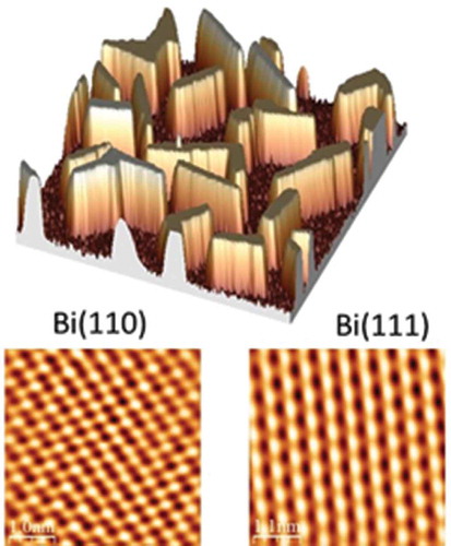
GRAPHICAL ABSTRACT
1. Introduction
Bismuth (Bi) has an atomic number of 83 and is generally considered the heaviest stable atom, with an extremely long radioactive -decay half-life of
years [Citation1]. Although Bi has five valence electrons (
), there exists a large separation between the s- and p-orbital energy levels. Thus, Bi generally behaves as an element with three valence electrons (i.e.,
), and the bulk element has a rhombohedral lattice structure [Citation2]. This rhombohedral structure can be regarded as a stretched face-centered cubic (fcc) structure along the body diagonal ()) [Citation3] and contains fewer symmetry elements than does the conventional fcc structure. The reduced symmetry pushes up the valence band maximum (VBM) at the T point and drags down the conduction band minimum (CBM) at the L point, although the valence and conduction bands are still separated by a continuous gap throughout the Brillouin zone. Consequently, the VBM and CBM overlap and Bi acts as a semimetal with a small Fermi surface associated with the electron and hole pockets [Citation4] (). These characteristics make Bi a material with a low effective carrier density and an extremely long Fermi wavelength. In addition, both the upper and lower band dispersions display linear k dependence at the band gap around the L point near the Fermi level
, which results in an extremely light effective carrier mass [Citation5]. The effective mass and its anisotropy have been reported in detail by Édel’man [Citation6]. These characteristic electronic states have made Bi a major playground in condensed matter physics for such important topics as diamagnetism [Citation7], giant magnetoresistance [Citation8], and the Shubnikov–de Haas effect [Citation9].
Figure 1. Crystalline and electronic structures of bulk Bi. (a) Rhombohedral structure. The basic lattice vectors in rhombohedral and hexagonal indices are indicated by the suffixes (Ro) and (Hex), respectively. In this article, we adopt the rhombohedral index. (b) Brillouin zone and (c) semimetallic band structure of bulk Bi with the rhombohedral structure. Reprinted with permission from (a) [Citation3], (b) [Citation15], and (c) [Citation21]
![Figure 1. Crystalline and electronic structures of bulk Bi. (a) Rhombohedral structure. The basic lattice vectors in rhombohedral and hexagonal indices are indicated by the suffixes (Ro) and (Hex), respectively. In this article, we adopt the rhombohedral index. (b) Brillouin zone and (c) semimetallic band structure of bulk Bi with the rhombohedral structure. Reprinted with permission from (a) [Citation3], (b) [Citation15], and (c) [Citation21]](/cms/asset/18f888af-259b-41f4-9a16-eae7370ad7e3/tapx_a_1845975_f0001_oc.jpg)
Recently, Bi has attracted considerable attention from the perspective of topological insulators. Band structure topology can be classified into two types, trivial and nontrivial, based on the index given by the product of parity of the wave function below the Fermi level at the time-reversal invariant momentum in the Brillouin zone [Citation10] for materials with space- and time-reversal symmetry such as Bi [Citation11]. The spin–orbit interaction (SOI) lifts the degeneracy of electron bands to open a gap. Furthermore, the SOI can invert the order of electron bands with different parities, such as the p-orbital-derived valence band and s-orbital-derived conduction band, to invert the sign of the
index. The SOI of an atom increases in proportion with the fourth power of Z [Citation12]. In this respect, Bi is the most promising candidate for developing topological insulators.
At the boundary of a topological insulator, the inverted band order reverts to the conventional configuration. Consequently, so-called topological edge states emerge along the boundary. In particular, a circuit of one-dimensional (1D) edge states arises along the periphery of two-dimensional (2D) topological insulators. The orientation of electron spin is constrained to be perpendicular to the direction of electron motion (spin-momentum locking) in the topological edge states [Citation10,Citation13,Citation14] making 2D topological insulators key materials for spintronics. For practical considerations, it is highly desirable to fabricate 2D insulators on Si substrates for Si-compatible spintronics. Thus, the nucleation and growth of ultrathin Bi films on Si substrates are of great importance. In this respect, we review the nucleation and growth of ultrathin Bi films mainly focusing on the Si(111) substrates. In the following, we first summarize the theories predicting that ultrathin Bi films of one or two bilayer thickness may serve as 2D topological insulators. Next, we review experimental findings concerning the nucleation and growth of ultrathin Bi islands and films on the extensively investigated Si(111) substrates. Finally, a summary is provided.
2. Theoretical prediction of Bi-based 2D topological insulators
2.1. Ultrathin Bi(111) films
In the bulk Bi crystal with the rhombohedral structure ()), (111) planes composed of a bilayer (BL) stack along the (111) direction [Citation15] as depicted in . The Bi atoms in each (111) BL are connected strongly by the nearest-neighbor covalent bonds, while the BLs are bonded by the much weaker second-nearest-neighbor bonds. Thus, the Bi(111) film behaves like a van der Waals material [Citation16–18] and the (111) surface is easily and stably exposed by cleavage. The Bi films preferentially grow along the (111) orientation.
Figure 2. (a) Top and (b) side views of the atomic arrangement in Bi(111) films with the bulk-like rhombohedral structure. The Bi atoms in the top bilayer are indicated by light and dark blue closed circles. The unit cell of the atomic arrangement in the Bi(111) plane is indicated by the light blue rhombus. Reprinted with permission from [Citation15]
![Figure 2. (a) Top and (b) side views of the atomic arrangement in Bi(111) films with the bulk-like rhombohedral structure. The Bi atoms in the top bilayer are indicated by light and dark blue closed circles. The unit cell of the atomic arrangement in the Bi(111) plane is indicated by the light blue rhombus. Reprinted with permission from [Citation15]](/cms/asset/762686f5-92f5-477f-a98f-9182fd819a39/tapx_a_1845975_f0002_oc.jpg)
In ultrathin Bi(111) films, the conduction and valence bands are quantized and pushed upward and downward, respectively. Consequently, the overlap of the conduction and valence bands in semimetallic bulk Bi is eliminated, and Bi(111) films are theoretically predicted to become semiconducting [Citation19] at thicknesses below 30 nm [Citation20]. However, this semimetal–semiconductor transition is difficult to detect in carrier transport experiments because the Bi(111) surface has larger electron and hole pockets than in the bulk [Citation17] and the surface conduction channel persists even in thin films. Nonetheless, the thickness-dependent evolution of the quantum well states (QWSs) has been successfully followed via angle-resolved photoelectron spectroscopy (ARPES) [Citation21–23], although the QWSs in the vicinity of the Fermi level were found to hybridize with two surface states at approximately in the surface Brillouin zone of ultrathin Bi(111) films. Experimentally, Bi(111) films were reported to be semiconducting even at thicknesses as large as 180 BL (for Bi(111), 1 BL = 0.39 nm) but become metallic again at thicknesses below 30 BL in an ARPES study [Citation24]. Similar behavior was recently observed in carrier transport experiments [Citation25,Citation26]. This return to the metallic state was speculated to be attributable to modification of the charge neutrality condition due to the thickness-dependent change of the surface state contribution.
As the film thickness is decreased, a one-BL-thick Bi(111) film will eventually be obtained. In such a film, the Bi atoms are arranged in a honeycomb lattice similar to graphene, as depicted in ). However, in contrast to graphene, the two Bi atoms in the 0.4540.454 nm
rhombic unit cell are inequivalent owing to the buckling in the BL ()). Graphene has been theoretically predicted to be a 2D topological insulator by Kane and Mele [Citation27]. However, its band gap is too small to be practically detected as a result of the very weak SOI of C atoms. A large SOI and breaking of the chiral symmetry of the honeycomb lattice due to buckling are effective ways to open the gap. Fortunately, one-BL-thick Bi(111) films have a large SOI and two inequivalent Bi atoms in the unit cell. Thus, they are expected to serve as 2D topological insulators. This behavior was confirmed by Murakami via theoretical calculations of the edge states [Citation28]. The results revealed that a one-BL-thick Bi(111) film has only one Kramers pair of the edge states, as expected for topologically nontrivial 2D materials. The nontrivial topology of a one-BL-thick Bi(111) film was further established by calculation of the topological index by Wada et al. [Citation29]. The topologies of Bi(111) films are expected to oscillate with the odd–even alternation of the BL thickness during film growth, if the inter-BL coupling is negligible [Citation28]. Taking the inter-BL coupling into consideration, Bi(111) films were theoretically predicted to be topologically nontrivial for up to eight BLs [Citation30], whereas thicker films become topologically trivial [Citation31]. Experimentally, one bilayer Bi(111) film was reported to be synthesized successfully on the
(111) substrate [Citation32]. Single layer Bi(111) film was also synthesized on the SiC(0001) substrate recently [Citation33].
2.2. Ultrathin Bi(110) films
Ultrathin Bi(110) films with the black phosphorus (BP)-like structure have also been theoretically predicted to be 2D topological insulators. In Bi(110) films, each Bi atom uses two of its three covalent bonds for the intralayer bonding in the (110) plane in the conventional bulk-like rhombohedral structure ()), while the remaining covalent bond is used for interlayer bonding ()). The rhombohedral Bi(110) surface can be regarded as the (100) surface of a pseudocubic lattice [Citation15]. Thus, half of the Bi atoms are slightly shifted downward in the (110) plane. The surface unit cell is defined as a rectangle with dimensions of 0.4540.475 nm
in which the slightly downward-shifted atom is situated at the center, as depicted in ). The Bi(110) layers are connected by ladder-like chains of covalent bonds along the (110) orientation in the rhombohedral structure, as shown in ). Therefore, energetically unfavorable dangling bonds are left on each Bi atom at the surface of the rhombohedral Bi(110) film.
Figure 3. (a) Top and (b) side views of the atomic arrangement in Bi(110) films with the bulk-like rhombohedral structure. (c) Corresponding Brillouin zone. Reprinted with permission from (a) [Citation34] and (b) [Citation15]
![Figure 3. (a) Top and (b) side views of the atomic arrangement in Bi(110) films with the bulk-like rhombohedral structure. (c) Corresponding Brillouin zone. Reprinted with permission from (a) [Citation34] and (b) [Citation15]](/cms/asset/7a0eff80-73a3-43e8-b150-46ef166c0d70/tapx_a_1845975_f0003_oc.jpg)
However, the formation energy of a Bi(110) film is predominantly governed by the surface energy rather than the bulk cohesive energy when the film thickness is sufficiently small. In this respect, the rhombohedral structure is considered to be energetically unfavorable for ultrathin Bi(110) films. Alternatively, ultrathin Bi(110) films were predicted to have a BP-like allotropic crystalline structure [Citation35]. In BP-like Bi(110) films, two Bi(110) layers form a pair to remove the dangling bonds, although this increases the out-of-plane buckling. The paired layers are stacked along the (110) orientation as depicted in ). As a result, BP-like Bi(110) films are exclusively composed of even numbers of layers, whereas Bi(110) films with the bulk-like rhombohedral structure may consist of even or odd numbers of layers. Furthermore, theoretical calculations have revealed that rhombohedral Bi(110) films with odd numbers of layers (N) are unstable and bifurcate into BP-like Bi(110) domains with even numbers of layers (N-1 and N +1) [Citation35].
Figure 4. Relation between the surface buckling and topological band gap. Atomic arrangements of Bi(110) films with the (a) bulk-like rhombohedral structure and (b) BP-like structure. (c) Top and side views of the atomic arrangement at the surface of BP-like Bi(110) films, where denotes the amplitude of the surface buckling. (d) Relation between the surface buckling and the band gap, where the topological transition occurs at
=0.1 Å. Reprinted with permission from (a,b) [Citation37] and (c,d) [Citation30]
![Figure 4. Relation between the surface buckling and topological band gap. Atomic arrangements of Bi(110) films with the (a) bulk-like rhombohedral structure and (b) BP-like structure. (c) Top and side views of the atomic arrangement at the surface of BP-like Bi(110) films, where h denotes the amplitude of the surface buckling. (d) Relation between the surface buckling and the band gap, where the topological transition occurs at h=0.1 Å. Reprinted with permission from (a,b) [Citation37] and (c,d) [Citation30]](/cms/asset/807e7609-94fd-4bbf-9cc3-bde758123a77/tapx_a_1845975_f0004_oc.jpg)
Lu et al. reported that one- and two-paired layer-thick Bi(110) films with the BP-like structure became 2D topological insulators with band gaps of approximately 100 and 50 meV, respectively, when the buckling of the surface atoms was sufficiently minor, on the basis of first-principles calculations [Citation30]. These predicted band gaps are larger than the thermal energy () at 300 K. In this respect, ultrathin BP-like Bi(110) films are anticipated to serve as 2D topological insulators even at room temperature.
The key to the topological nature of BP-like Bi(110) films is the small amplitude of the buckling of the surface atoms ()). The and
orbital-derived bands are already inverted by the strong crystal field in BP-like Bi(110) films, although they become degenerate at a
point on the
-
line. This degeneracy is lifted by the SOI to open a gap
. Thus, BP-like Bi(110) films can intuitively be expected to serve as 2D topological insulators. However, the surface buckling breaks the inversion symmetry and reduces the topological band gap. Theoretical calculations have indicated that the topological band gap is closed at a surface buckling of 0.01 nm. Upon further increasing the surface buckling, the band order of the
and
bands is reverted and the Bi(110) films become topologically trivial insulators as shown in ) [Citation30]. Thus, one- and two-paired layer-thick Bi(110) films are expected to be 2D topological insulators only in the case that they have a BP-like structure and very low surface buckling. The topological band gap was reported to decrease with increasing film thickness for buckling-free BP-like Bi(110) films according to theoretical calculations [Citation30]. The topological gap closes and the film becomes topologically trivial at thicknesses exceeding three paired layers [Citation30]. In contrast, one-paired layer-thick Bi(110) films were previously reported to be topologically trivial on the basis of theoretical calculations by Wada et al. [Citation29]. However, the effects of surface buckling were not considered in that study. Calculations have been performed for Bi(110) films with an ordinal surface buckling. In this respect, the results do not contradict the findings of Lu and co-workers. In a recent experiment, the Bi(110) film on the graphite substrate was reported to have an extremely small buckling less than 0.004
0.0005 nm [Citation36].
3. Nucleation and growth of ultrathin Bi films on Si(111) substrates
3.1. Preferential orientations
Epitaxial growth of Bi films take place at room temperature on Si substrates. Intuitively, ultrathin Bi(111) films are expected to be obtained by the epitaxial growth on the Si(111) substrates. However, Nagao et al. found that not the Bi(111) but the Bi(110) islands nucleate in the initial stage of the epitaxial growth on Si(111)77 substrates at room temperature [Citation37–40]. The nucleation of Bi(110) islands is not limited to film growth on Si(111)7
7 substrates, but has also been widely observed during the initial stages of Bi film growth on a wide variety of other substrates, such as Si(111)
-B [Citation34,Citation41], Si(111)
-
-Bi [Citation42,Citation43], Ge(111)c(2
8) [Citation44], W(110) [Citation45], highly oriented pyrolytic graphite (HOPG) [Citation46–50], Nb
[Citation51], and icosahedral Al-Pd-Mn quasicrystals [Citation52]. The Bi(110) islands were observed to be predominantly composed of even numbers of layers on the Si(111)7
7,
-B, and
-
-Bi substrates. Thus, Bi(110) islands have been recognized to have the BP-like structure rather than the bulk-like rhombohedral structure.
The nucleation of BP-like Bi(110) islands is attributed to the low surface energy due to the lack of dangling bonds. The free-energy cost upon nucleation G can be fundamentally expressed as
[Citation53]. Here,
,
, V,
, and A are the change in chemical potential upon nucleation, surface energy of the island per unit area, volume of the island, atomic volume in the crystal, and surface area of the island, respectively. In addition, the edge formation energy can contribute to the cost of the free energy. However, its difference between the Bi(111) and (110) islands has not been well understood at present. Thus, we omit the contribution of the edge formation energy in the following. The significance of this equation is that
G is determined by the balance of the energy gain upon the incorporation of Bi atoms into the island volume and the energy loss due to the formation of the surface and interface. As the island size
changes, V varies in proportion to
while
varies in proportion to
. Thus, the contribution of the second surface term becomes dominant over the energy gain with the incorporation of Bi atoms into the island volume for small
values. Therefore, ultrathin Bi islands are considered to have a BP-like Bi(110) structure with an extremely low surface energy during the initial stage of nucleation on various substrates.
However, atoms are forced to buckle to form the paired layers in the BP-like structure. This introduces strain into the lattice and increases the chemical potential in the bulk [Citation35,Citation37]. Bi atoms preferentially adopt the bulk-like structure with lower strain with respect to incorporation into the island. The first volumetric term dominates over the second surface term at larger values in the above equation for
G. Consequently, the transition from the BP-like structure to the bulk-like rhombohedral structure occurs at a certain ‘critical thickness’ during the growth of the Bi film.
Specifically, BP-like Bi(110) islands were observed to transform into bulk-like Bi(111) islands at a critical thickness of 4 ML (= 2 paired layer) on the Si(111)77 substrate by low-energy electron diffraction (LEED) and scanning tunneling microscopy (STM) [Citation37]. In the initial stage, atomically flat Bi islands nucleated on the Si(111)7
7 substrate at a coverage of
4 ML, as shown by the STM image in . These were confirmed to be Bi(110) islands by the observation of the characteristic atomic arrangement of the Bi(110) surface on the tops of the islands (inset in )). In , the orientation of the Bi islands is indicated using the hexagonal index, in which the (012) and (001) orientations correspond to the (110) and (111) orientations, respectively, in our rhombohedral index. The Bi(110) islands were determined to have a BP-like structure because they were composed of even numbers of layers according to the STM images. The BP-like Bi(110) islands displayed a random in-plane orientation, leading to ring-like LEED diffraction patterns as shown in ). However, the ring-like Bi(110) diffraction patterns changed to Bi(111) diffraction spots at
6 ML, as shown in ). The hexagonal arrangement of the Bi(111) surface was also observed at the tops of these islands by STM () and its inset). The structural transition reached completion at 4
6 ML, where the BP-like Bi(110) and the bulk-like Bi(111) islands coexisted as observed by both LEED and STM (). The structural transition from BP-like Bi(110) to bulk-like Bi(111) was quantitatively reproduced in theoretical calculations for a free-standing Bi film. ) presents the thickness dependence of the theoretically calculated cohesive energy for BP-like Bi(110) and bulk-like Bi(111) islands. The cohesive energy of the BP-like Bi(110) islands was higher than that of the bulk-like Bi(111) islands for thicknesses below 4 ML, whereas the opposite was observed for larger thicknesses [Citation37]. This means that the structural transition occurs at
= 4 ML, as observed in the experiment. The structural transition from Bi(110) to Bi(111) has been experimentally observed to occur not only on the Si(111)7
7 substrate but also on a variety of other substrates, such as Si(111)
-B [Citation54], Si(111)
-
-Bi [Citation39,Citation42], Ge(111)c(2
8) [Citation44], and HOPG [Citation46].
One exception for which this structural transition does not occur is the growth of Bi on the (111) substrate. On this substrate, bulk-like Bi(111) islands were found to grow from the beginning [Citation32,Citation55,Citation56]. This finding was ascribed to the high similarity between the lattice constant of the
(111) surface (0.438 nm) and that of the Bi(111) surface (0.454 nm). Furthermore, the
(111) surface has the same threefold rotational symmetry as the Bi(111) plane. The growth of single layer Bi(111) film was also reported on the SiC(0001) substrate recently [Citation33]. However, for most substrates that do not satisfy this condition, a BP-like Bi(110) film with low surface energy nucleates initially and then transforms to bulk-like Bi(111) islands at a certain critical thickness.
Figure 5. Nucleation and growth of Bi islands on a Si(111)77 substrate at room temperature. (a,c,e) and (b,d,f) show LEED and STM results, respectively. The Bi coverage was 2–4 ML in (a,b), 4–6 ML in (c,d), and greater than 6 ML in (e,f). (g) Theoretically calculated thickness dependence of the cohesive energy of BP-like Bi(110) and bulk-like Bi(111) films. The crystal orientation is indicated using the hexagonal index; the {012} and {001} orientations in the hexagonal index correspond to the (110) and (111) orientations in the rhombohedral index. Reprinted with permission from [Citation37]
![Figure 5. Nucleation and growth of Bi islands on a Si(111)7×7 substrate at room temperature. (a,c,e) and (b,d,f) show LEED and STM results, respectively. The Bi coverage was 2–4 ML in (a,b), 4–6 ML in (c,d), and greater than 6 ML in (e,f). (g) Theoretically calculated thickness dependence of the cohesive energy of BP-like Bi(110) and bulk-like Bi(111) films. The crystal orientation is indicated using the hexagonal index; the {012} and {001} orientations in the hexagonal index correspond to the (110) and (111) orientations in the rhombohedral index. Reprinted with permission from [Citation37]](/cms/asset/71b6f7c4-1809-44db-b8df-d74dd1ce3013/tapx_a_1845975_f0005_oc.jpg)
3.2. Nucleation and growth of Bi(110) films
The initial nucleation of Bi(110) islands is recognized to be a consequence of the low surface energy of the BP-like structure. This recognition is experimentally supported by the even numbers of layers observed by STM for the nucleated Bi(110) islands [Citation37]. The BP-like Bi(110) islands are composed of stacked paired layers with strictly even numbers of layers. Theoretical calculations also indicate a BP-like structure for the Bi(110) islands [Citation35]. However, a step-and-terrace structure with a height of one ML was observed for Bi(110) islands on a Ge(111)c(28) substrate [Citation44]. The Bi(110) islands with the height of odd numbers of layers were also observed on the Si(111)-
-
-Bi substrate [Citation42]. Although BP-like Bi(110) films exclusively contain even numbers of layers, bulk-like Bi(110) films may be composed of even or odd numbers of layers. Thus, the above result suggests that Bi(110) islands have a bulk-like structure rather than a BP-like structure, casting doubt on the conventional interpretation of the preferential nucleation of Bi(110) films with a BP-like structure. However, both BP-like and bulk-like Bi(110) islands have the same atomic arrangement at their surfaces, as depicted in . Thus, these two structures cannot be distinguished by either LEED or atomically resolved STM images.
The above problem was addressed in an STM study on the growth of Bi(110) islands on the Si(111)-B substrate at room temperature [Citation34]. As shown in ), the STM images revealed the nucleation of rod-shaped Bi(110) islands on this substrate. The Bi(110) islands had atomically flat surfaces and exhibited the characteristic atomic arrangement of the Bi(110) plane, as depicted in the inset. The islands extended along one of six specific in-plane orientations on the Si(111)
-B substrate ()), whereas they were orientated randomly on the Si(111)7
7 substrate [Citation37]. The Bi(110) islands persisted to a height exceeding 20 MLs during growth on Si(111)
-B at a low deposition rate of 0.035 ML/min. The evolution of the area ratios of Bi(110) islands with heights ranging from 4 to 20 MLs is shown by the histogram presented in ). The Bi(110) islands were predominantly composed of even numbers of layers (indicated by the red bars), as reported for growth on the Si(111)7
7 substrate [Citation37]. However, detailed analysis of the height distribution of the Bi(110) islands revealed that a small number of Bi(110) islands containing odd numbers of layers (indicated by the blue bars) always coexisted with the Bi(110) islands containing even numbers of layers.
The dominance of the Bi(110) islands composed of even numbers of layers can be reasonably ascribed to the BP-like structure with a low surface energy. However, this conflicts with the observed coexistence of islands containing odd numbers of layers, which suggests that the Bi(110) islands have a bulk-like structure during growth irrespective of their height. Nonetheless, a four-ML-thick Bi(110) film on the Si(111)-B substrate was recently confirmed to have the BP-like structure by surface X-ray diffraction [Citation54]. It may be the case that the Bi(110) islands alternate between the BP-like and bulk-like structures with the variation between even and odd numbers of layers during growth. However, this seems unlikely owing to the energetic preference of the BP-like structure for ultrathin Bi(110) islands.
Figure 6. Nucleation of Bi(110) islands on the Si(111)-B substrate. (a) Typical STM image of the nucleated Bi(110) islands for a Bi coverage of 5.6 MLs. Inset: atomically resolved STM image of the surface of a Bi(110) island. (b) Six preferred in-plane orientations of the nucleated Bi(110) islands. (c) Evolution of the height distribution of the Bi(110) islands. The distributions are magnified tenfold at greater heights for clarity, as indicated by the dashed bars. (d) STM image of a six-ML-thick Bi(110) island with a single-layer terrace. (e) High-resolution STM image of the atomic arrangement in the vicinity of the edge between six- and seven-ML-thick regions. (f) Ball-and-stick model of the atomic structure of the island with six- and seven-ML-thick regions. The six-ML-thick region has the BP-like structure, whereas the seven-ML-thick region has a sandwich structure. Reprinted with permission from [Citation34]
![Figure 6. Nucleation of Bi(110) islands on the Si(111)√3×√3-B substrate. (a) Typical STM image of the nucleated Bi(110) islands for a Bi coverage of 5.6 MLs. Inset: atomically resolved STM image of the surface of a Bi(110) island. (b) Six preferred in-plane orientations of the nucleated Bi(110) islands. (c) Evolution of the height distribution of the Bi(110) islands. The distributions are magnified tenfold at greater heights for clarity, as indicated by the dashed bars. (d) STM image of a six-ML-thick Bi(110) island with a single-layer terrace. (e) High-resolution STM image of the atomic arrangement in the vicinity of the edge between six- and seven-ML-thick regions. (f) Ball-and-stick model of the atomic structure of the island with six- and seven-ML-thick regions. The six-ML-thick region has the BP-like structure, whereas the seven-ML-thick region has a sandwich structure. Reprinted with permission from [Citation34]](/cms/asset/9c032245-3ae1-4e58-a811-050e78321a81/tapx_a_1845975_f0006_oc.jpg)
The mystery regarding the Bi(110) islands containing odd numbers of layers would be solved by a sandwich structure, in which Bi(110) islands with odd numbers of layers occur as one-ML-thick terrace regions on top of Bi(110) islands with even numbers of layers. For example, ) presents an STM image of a seven-ML-thick Bi(110) terrace on a six-ML-thick Bi(110) island. The unit cells of the six- and seven-ML-thick regions of the Bi(110) surface were demonstrated to be aligned across the step edge via atomically resolved STM, as shown in ). However, neither the combination of BP-like six-ML-thick and bulk-like seven-ML-thick Bi(110) islands nor the combination of bulk-like six-ML-thick and bulk-like seven-ML-thick islands would account for such an in-phase alignment of the unit cells across the step edge. The in-phase alignment can only be explained by the combination of BP-like six-ML-thick and sandwich-structured seven-ML-thick Bi(110) islands, as depicted in the top view of ) [Citation34]. The sandwich structure was originally proposed for the Bi(110) films on an HOPG substrate on the basis of density functional theory (DFT) calculations [Citation47,Citation49]. In the sandwich-structured Bi(110) islands, the inner layers have the bulk-like structure but the top and bottom surfaces are terminated by a paired layer with the BP-like structure, as indicated in the cross-sectional view of ). The inner bulk-like structure and outer BP-like single BL are connected by hypervalent bonds. Owing to the BP-like surface layer, the Bi(110) islands containing odd numbers of layers have a comparably low surface energy as those containing even numbers of layers. Thus, ultrathin Bi(110) islands with odd numbers of layers have a sandwich structure. However, the introduction of the hypervalent bonds is associated with increased energy costs for the incorporation of the Bi atoms into the sandwich-structured islands. This reasonably accounts for the relatively low proportion of the Bi(110) islands containing odd numbers of layers that coexist with the BP-like Bi(110) islands during the initial nucleation and growth process.
The occurrence of a sandwich structure for the Bi(110) islands containing odd numbers of layers is experimentally supported by scanning tunneling spectroscopy (STS) results. At the surface of the bulk-like Bi(110) structure, a dangling bond protrudes from each surface atom. The
states form a Dirac-cone-like surface dispersion in the vicinity of the Fermi level at the
point on the bulk-like Bi(110) surface owing to the interplay between mirror symmetry and the SOI [Citation38]. On the other hand, a gap opens near the Fermi level on the BP-like Bi(110) surface, where all of the
bonds are utilized to form the paired BL. DFT calculations revealed that this difference in the surface-state dispersion is reflected in the density of states (DOS) near the Fermi level [Citation35]. A gap opens in the DOS at the BP-like Bi(110) surface, whereas this gap is closed at the Bi(110) surface with the bulk-like structure. Furthermore, the gap was found to remain for Bi(110) islands with both even and odd numbers of layers by STS [Citation34]. These results indicate that Bi(110) islands containing odd numbers of layers also have the BP-like paired layer structure at the top surface, as expected for the sandwich structure.
During the growth of Bi(110) islands, both one- and two-ML-thick terraces have been observed on Bi(110) islands with even numbers of layers. The two-ML-thick terraces were dominant, while the one-ML-thick terraces were a minor component. On the other hand, neither one- nor two-ML-thick terraces were observed on Bi(110) islands containing odd numbers of layers. These observations were ascribed to the lower energetic stability of the Bi(110) islands with odd numbers of layers, which caused the one-ML-thick terraces on these islands to immediately revert to the more energetically favorable BP-like structure. Thus, the Bi(110) islands are expected to grow with alternation of the structure between the BP-like and sandwich structures as the number of layers varies between even and odd.
Besides the preference for even numbers of layers, that is, vertical size, Bi(110) islands have been reported to preferentially display specific widths on HOPG substrates [Citation47]. For example, six-ML-thick Bi(110) islands were observed to preferentially have widths of 12, 16, and 20 nm, corresponding to a spacing of 4 nm. This preference for specific lateral sizes is attributed to the quantum size effect (QSE). Actually, the 4 nm spacing is consistent with half of the Fermi wavelength
, which is defined by the electron pockets located between
and
. The observed preferred widths thus match
, where
is an integer as expected for QSE. The spacing between the preferred widths was found to increase with increasing Bi(110) island height, which was ascribed to the height-dependent change of
with electron doping from the HOPG substrate to the Bi(110) islands [Citation47]. Although the QSE of the island width has not been investigated on the Si(111) substrate, this phenomenon is expected to occur ubiquitously.
From the perspective of realizing 2D topological insulators, the Bi(110) islands must theoretically have the BP-like structure, a height of one or two BLs, and a low surface buckling of less than 0.01 nm [Citation30]. We can easily obtain Bi(110) islands that satisfy the first two requirements on Si(111) substrates by adjusting the amount of deposited Bi atoms during growth at room temperature. However, the surface buckling was observed to be as large as 0.03 nm for Bi(110) islands on the Si(1111)-B substrate [Citation41]. A similar degree of surface buckling was reported for Bi(110) islands on the 4 H-SiC(0001) substrate [Citation50]. In contrast, the surface buckling was found to be one order of magnitude smaller for Bi(110) islands on the HOPG substrate. Kowalczyk
reported the buckling was smaller than 0.004
0.0005 nm [Citation36]. The BP-like Bi(110) islands with a thickness of 2 ML (= 1 BL) on the HOPG substrate were observed to display gapless states at the edge, as expected for a 2D topological insulator [Citation30]. Furthermore, DFT calculations revealed that BP-like Bi(110) islands with low surface buckling became stable upon electron doping to populate electron bands close to the Fermi level [Citation30]. In fact, electron doping occurs efficiently on the HOPG substrate but not on epitaxial graphene [Citation30]. The Si(111)
-B substrate dopes holes but not electrons to the interface states [Citation57]. Thus, the key to achieving low surface buckling is considered to be electron doping from the HOPG substrate to the Bi(110) islands. For electron doping to ultrathin BP-like Bi(110) islands, n-type Si(111) substrates with extremely high carrier concentrations are expected to be suitable. The
Si(111)7
7 substrate was found to hinder the Peierls transition of 1D In atomic chains on the surface owing to electron doping [Citation57]. Furthermore, it may be possible to dope electrons into BP-like Bi(110) films [Citation58] on conventional Si-on-insulator substrates using the back gate. Therefore, it is anticipated to be possible to realize 2D topological insulators based on Bi(110) films on Si substrates via these methods.
3.3. Wetting layer and commensuration
During the growth of Bi films on Si, the Si substrate is initially covered by an amorphous one-ML-thick wetting layer, upon which the Bi(110) and Bi(111) islands nucleate. The Bi atoms in the wetting layer do not exhibit any long-range ordering [Citation34,Citation40]. In STM, the height of the Bi islands is measured from the wetting layer. Nevertheless, as described in the previous subsection, the Bi(110) islands were observed to preferentially contain even numbers of layers owing to the BP-like structure with the stacking of paired BLs. This means that the wetting layer serves as a buffer layer that separates the overlying Bi(110) islands from the substrate.
Because the Bi atoms have a random arrangement without long-range order in the wetting layer, the subsequently nucleated Bi(110) islands are not expected to align along specific in-plane orientations. Actually, Bi(110) islands afforded a ring-like LEED pattern with random in-plane orientation on the Si(111)77 substrate [Citation37]. In contrast, Bi(110) islands on the
-B substrate were found to orient along one of six specific orientations, as depicted in [Citation34,Citation41]. The same phenomenon was observed on the Si(111)
-Bi substrate. The Bi(110) islands transform to Bi(111) islands at a certain critical thickness on these Si(111)7
7,
-B, and
-Bi substrates, and the in-plane lattice vectors of the transformed Bi(111) islands appear to align along the threefold rotational axis of the Si(111)1
1 substrate lattice on all of these substrates. However, the Bi islands would not adopt specific orientations on the wetting layer in the absence of any in-plane periodicity. Thus, it is suggested that the Bi atoms in the wetting layer undergo local periodic rearrangement to register the Bi islands to the underlying Si(111) substrates. Actually, the
tetramer clusters were reported to be decomposed easily into a substrate registered ordered phase at around room temperature on the Ag(001) substrate [Citation59]. The local crystallization of the amorphous wetting layer under ultrathin films was also confirmed via surface X-ray diffraction in the case of Ag film growth on the Si(111)7
7 substrate [Citation60,Citation61].
On Si(111) substrates, the diagonal of the Bi(110) rectangular unit cell is commensurate with that of the rhombic Si(111)
unit cell with a ratio of 7:4 along the
1
0
direction. However, either of the two diagonals of the rectangular unit cell of the Bi(110) islands may align along any of the three rotationally equivalent
1
0
axes of the Si(111) substrate. The long side of the Bi(110) rectangular unit cell thus orients along ±
from the Si
1
0
direction depending on the choice of diagonal. This adequately accounts for the alignment of the Bi(110) islands along the six preferential orientations on the Si(111)
substrates [Citation41]. However, this commensurate relation does not hold for the Si(111)7
7 substrate, upon which the in-plane orientations of the Bi(110) islands are random. In the case of the Bi(111) islands, the Bi(111) rhombic unit cell is commensurate with that of the Si(111)1
1 lattice with a ratio of 6:7. Thus, Bi(111) islands are considered to nucleate with threefold rotational symmetry similar to that on the Si(111) surface.
The lattice commensuration at the Bi–Si interface could exert an influence on the stability of the Bi(110) islands and the critical thickness of the structural transition from Bi(110) to Bi(111). However, there is no noticeable difference in the critical thickness between the Si(111)77 and
-Bi substrates. The critical thickness on the Si(111)7
7 substrate was reported to be 4 and 6 MLs on the basis of STM [Citation37] and ARPES [Citation38], respectively, while the critical thickness on the Si(111)
-Bi substrate was found to be approximately 6 MLs [Citation39,Citation42]. This insensitivity of the critical thickness is also supported by theoretical calculations of Bi films in which the bottom layer was terminated by hydrogen atoms in various ways [Citation37]. The critical thickness instead appears to be dependent on the deposition rate. The deposition rate was 0.3–0.4 ML/min in the above experiments on the Si(111)7
7 [Citation37] and
-Bi substrates [Citation39,Citation42] where the critical thickness was reported to be approximately 4–6 MLs. In contrast, the critical thickness on the Si(111)
-B substrate was found to exceed 40 MLs in an experiment using a deposition rate of 0.035 ML/min. This extremely large critical thickness is not a unique feature of the
-B substrate. The critical thickness was observed to decrease with increasing deposition rate [Citation62]. These results suggest that Bi(110) islands become persistent for some kinetic reason at low deposition rates, although the details have not yet been elucidated.
The negligible influence of the interfacial commensuration on the critical thickness is attributed to the wide spacing between the Bi film and the wetting layer in reality. A surface X-ray diffraction study revealed that the spacing between the wetting layer and the overlying Bi film was 36 greater than that between the (111) BLs in a 15-ML-thick Bi(111) film on a Si(111)7
7 substrate [Citation63]. This permits the Bi(111) film to exhibit bulk-like lattice parameters. Owing to the weak substrate interaction and the strain-free structure, Bi(111) films on the Si(111)7
7 substrate are actually free standing. Indeed, the bulk band dispersion experimentally determined from the thickness-dependent change of QWSs in ARPES spectra was found to be mostly consistent with that obtained from DFT calculations for free-standing Bi films [Citation64]. However, the electronic states of rhombohedral Bi films are sensitive to strain. For example, a Bi(111) film on the Bi
Te
(111) substrate was found to be laterally expanded by 3
[Citation65]. It was reported that the topological nature of ultrathin Bi(111) films changes in response to substrate-derived strain [Citation65]. In this respect, it is crucial to consider the strain due to the interface in Bi films, although this effect is anticipated to be less drastic on Si(111) substrates.
4. Summary
Ultrathin Bi films grow epitaxially on Si(111) substrates at room temperature. The Si substrates are initially covered by a one-ML-thick wetting layer, upon which Bi(110) islands subsequently nucleate. The Bi(110) islands are preferentially composed of an even number of layers, although a small proportion of the islands contain odd numbers of layers. The dominance of the Bi(110) islands with even numbers of layers height is attributed to the BP-like structure which is composed of the stacking of paired layers. The Bi(110) islands containing odd numbers of layers have a sandwich structure in which the bulk-like rhombohedral structure is surrounded on the top and bottom by BLs with the BP-like structure. With further growth, the Bi(110) islands transform to Bi(111) islands with a bulk-like rhombohedral structure at a certain critical thickness. The wetting layer serves as a buffer layer that separates the overlying Bi film from the Si(111) substrate by providing a wide spacing with the bottom of the overlying Bi islands. The initial nucleation of the BP-like Bi(110) islands, the sandwich structure of the minority Bi(110) islands containing odd numbers of layers, and the transformation from Bi(110) islands to Bi(111) islands are all governed by the thickness-dependent energy balance between surface formation and atom incorporation into the Bi islands.
Disclosure statement
No potential conflict of interest was reported by the author.
References
- Tavares AP, Medeiros EL, Terranova ML. Alpha decay half-life of bismuth isotopes. J Phys G Nucl Part Phys. 2005;31:129.
- Fukaya Y. Bussei-kenkyu. A historical review of the study on Bismuth. 2008;90:537–21. (in Japanese).
- Song TE, Wilde G, Peterlechner M. Morphology and aspect ratio of bismuth nanoparticles embedded in a zinc matrix. Appl Phys Lett. 2014;105:241902.
- Liu Y, Allen RE. Electronic structure of the semimetals Bi and Sb. Phys Rev B. 1995;52:1566.
- Fuseya Y, Ogata M, Fukuyama H. Transport properties and diamagnetism of dirac electrons in bismuth. J Phys Soc Jpn. 2015;84:012001.
- Édel’man VS. Electrons in bismuth. Adv Phys. 1976;25:555.
- Kamerlingh Onnes H, Beckman B. Comm Phys Lab Leiden. On the HALL effect and the change in the resistance in a magnetic field at low temperatures. II. The HALL-effect and the resistance increase for bismuth. 1912;129a:3.
- Kapitza P. Proc Roy Soc A. The study of the specific resistance of bismuth crystals and its change in strong magnetic fields and some allied problems. 1928;119:369.
- L.V. Shubnikov and W.J. de Haas, A new phenomenon in the change of resistance in a magnetic field of single crystals of bismuth, Nature 126 (1930) 500.
- Fu L, Kane CL. Topological insulators with inversion symmetry. Phys Rev B. 2007;76:045302.
- Lin Z, Lin CX, Wu YS, et al. Stable Nontrivial Z2Topology in Ultrathin Bi (111) Films: A First-Principles Study. Phys Rev Lett. 2011;107:136805.
- Steinfeld JI. Molecules and radiation. Cambridge: MIT Press; 1985.
- Moore JE. The birth of topological insulators. Nature. 2010;464:194.
- Hasan MZ, Kane CL. Colloquium: topological insulators. Rev Mod Phys. 2010;82:3045.
- Hofmann P. The surfaces of bismuth: structural and electronic properties. Prog Surf Sci. 2006;81:191.
- Möonig H, Sun J, Koroteev M, et al. Structure of the (111) surface of bismuth: LEED analysis and first-principles calculations. Phys Rev B. 2005;72:085410.
- Ast CR, Höchst H. Electronic structure of a bismuth bilayer. Phys Rev B. 2003;67:113102.
- Koroteev YM, Bihlmayer G, Chulkov EV, et al. First-principles investigation of structural and electronic properties of ultrathin Bi films. Phys Rev B. 2008;77:045428.
- Sandomirskii VB. Quantum Size Effect in a Semimetal Film. Sov Phys. 1967;25:101.
- Ogrin YF, Lutskii VN, Elinson MI. Observation of Quantum Size Effects in Thin Bismuth Films. JETP Lett. 1966;3:71.
- Hirahara T. The Rashba and quantum size effects in ultrathin Bi films. J Electron Spectroscopy Related Phenomena. 2015;201:98.
- Ito S, Feng B, Arita M, et al. Proving nontrivial topology of pure bismuth by quantum confinement. Phys Rev Lett. 2016;117:236402.
- Bian G, Wang X, Kowalczyk PJ, et al. Survey of electronic structure of Bi and Sb thin films by first-principles calculations and photoemission measurements. J Phys Chem Solids. 2019;128:109.
- Hirahara T, Shirai T, Hajiri T, et al. Role of quantum and surface-state effects in the bulk fermi-level position of ultrathin Bi films. Phys Rev Lett. 2015;115:106803.
- Xiao S, Wei D, Jin X. Bi(111) thin film with insulating interior but metallic surfaces. Phys Rev Lett. 2012;109:166805.
- Aitani M, Hirahara T, Ichinokura S, et al. In situ magnetotransport measurements in ultrathin Bi films: evidence for surface-bulk coherent transport. Phys Rev Lett. 2014;113:206802.
- Kane CL, Mele EJ. Quantum spin hall effect in graphene. Phys Rev Lett. 2005;95:226801.
- Murakami S. Quantum spin hall effect and enhanced magnetic response by spin-orbit coupling. Phys Rev Lett. 2006;97:236805.
- Wada M, Murakami S, Freimuth F, et al. Localized edge states in two-dimensional topological insulators: ultrathin Bi films. Phys Rev B. 2011;83:121310(R).
- Lu Y, Xu W, Zeng M, et al. Topological properties determined by atomic buckling in self-assembled ultrathin Bi(110). Nano Lett. 2015;15:80.
- Yeom HW, Jin KH, Jhi SH. Topological fate of edge states of single Bi bilayer on Bi(111). Phys Rev B. 2016;93:075435.
- Hirahara T, Bihlmayer G, Sakamoto Y, et al. Interfacing 2D and 3D topological insulators: Bi(111) Bilayer on Bi2Te3. Phys Rev Lett. 2011;107:166801.
- Reis F, Li G, Dudy L, et al. Bismuthene on a SiC substrate: A candidate for a high-temperature quantum spin hall material. Science. 2017;357:287.
- Nagase K, Kokubo I, Yamazaki S, et al. Structure and growth of Bi(110) islands on Si(111)√3x √3−B substrates. Phys Rev B. 2018;97:195418.
- Bian G, Wang X, Miller T, et al. First-principles and spectroscopic studies of Bi(110) films: thickness-dependent Dirac modes and property oscillations. Phys Rev B. 2014;90:195409.
- Kowalczyk PJ, Brown SA, Maerkl T, et al. Realization of symmetry-enforced two-dimensional dirac fermions in nonsymmorphic α-bismuthene. ACS Nano. 2020;14:1888.
- Nagao T, Sadowski JT, Saito M, et al. Nanofilm allotrope and phase transformation of ultrathin Bi film on Si(111)-7×7. Phys Rev Lett. 2004;93:105501.
- Bian G, Miller T, Chiang T-C. Electronic structure and surface-mediated metastability of Bi films on Si(111)-7×7 studied by angle-resolved photoemission spectroscopy. Phys Rev B. 2009;80:245407.
- Yaginuma S, Nagaoka K, Nagao T, et al. Electronic structure of ultrathin bismuth films with A7 and Black-phosphorus-like structures. J Phys Soc Jpn. 2008;77:014701.
- Sadowski JT, Nagao T, Yaginuma S, et al. Stability of the quasicubic phase in the initial stage of the growth of bismuth films on Si(111)-7×7. J Appl Phys. 2006;99:014904.
- Kokubo I, Yoshiike Y, Nakatsuji K, et al. Ultrathin Bi(110) films on Si(111)√3x √3−B substrates. Phys Rev B. 2015;91:075429.
- Yaginuma S, Nagao T, Sadowski JT, et al. Origin of flat morphology and high crystallinity of ultrathin bismuth films. Surf Sci. 2007;601:3593.
- Lükermann D, Banyoudeh S, Brand C, et al. Growth of epitaxial Bi-films on vicinal Si(111). Surf Sci. 2014;621:82.
- Hatta S, Ohtsubo Y, Miyamoto A, et al. Epitaxial growth of Bi thin films on Ge(111). Appl Surf Sci. 2009;256:1252.
- Koitzsch C, Bovet M, Clerc F, et al. Growth of thin Bi films on W. Surf Sci. 2003;527:51.
- Scottt SA, Kral MV, Brown SA. A crystallographic orientation transition and early stage growth characteristics of thin Bi films on HOPG. Surf Sci. 2005;587:175.
- Kowalczyk PJ, Mahapatra O, Brown SA, et al. Electronic size effects in three-dimensional nanostructures. Nano Lett. 2013;13:43.
- Kowalczyk PJ, Mahapatra O, McCarthy DN, et al. STM and XPS investigations of bismuth islands on HOPG. Surf Sci. 2011;605:659.
- Kowalczyk PJ, Belic D, Mahapatra O, et al. Anisotropic oxidation of bismuth nanostructures: evidence for a thin film allotrope of bismuth. Appl Phys Lett. 2012;100:151904.
- Sun JT, Huang H, Wong SL, et al. Energy-gap opening in a Bi(110) nanoribbon induced by edge reconstruction. Phys Rev Lett. 2012;109:246804.
- Peng L, Xian JJ, Yang R, et al. Visualizing topological edge states of single and double bilayer Bi supported on multibilayer Bi(111) films. Phys Rev B. 2018;98:245108.
- Sharme HR, Fournée V, Shimoda M, et al. Growth of Bi thin films on quasicrystal surfaces. Phys Rev B. 2008;78:155416.
- Saito Y. Statistical physics of crystal growth. Singapore: World Scientific; 1996.
- Nagase K, Ushioda R, Nakatsuji K, et al. Growth of extremely flat Bi(110) films on a Si(111)√3 × √3-B substrate. Appl Phys Exp. 2020;13:085506.
- Yang F, Miao L, Wang ZF, et al. Spatial and energy distribution of topological edge states in single Bi(111) bilayer. Phys Rev Lett. 2012;109:016801.
- Chen M, Peng J-P, Zhang H-M, et al. Molecular beam epitaxy of bilayer Bi(111) films on topological insulator Bi2Te3: A scanning tunneling microscopy study. Appl Phys Lett. 2012;101:081603.
- Ogino T, Kuzumo VM, Yamazaki S, et al. Variation of the metal-insulator transition temperature of quasi-one-dimensional indium chains upon carrier doping from Si(111) substrates. J Phys: Cond Matter. 2020;32:415001.
- Li -S-S, Ji WX, Hu SJ, et al. Tunability of the Quantum Spin Hall Effect in Bi(110) Films: effects of Electric Field and Strain Engineering. ACS Appl Matter Interf. 2017;9:21515.
- Nakagawa T, Ohgami O, Saito Y, et al. Transition between tetramer and monomer phases driven by vacancy configuration entropy on Bi∕Ag(01). Phys Rev B. 2007;75:155409.
- Chen Y, Gramlich MW, Hayden ST, et al. Critical role of a buried interface in the Stranski-Krastanov growth of metallic nanocrystals: quantum size effects in Ag/Si(111)-(7×7). Phys Rev Lett. 2015;114:035501.
- Chen Y, Gramlich MW, Hayden ST, et al. In situ x-ray scattering study of Ag island growth on Si(111)7×7. Phys Rev B. 2016;94:045437.
- Ushioda R, Shirasawa T, Nakatsuji K, et al. in preparation
- Shirasawa T, Ohyama M, Voegeli W, et al. Interface of a Bi(001) film on Si(111)−7×7 imaged by surface x-ray diffraction. Phys Rev B. 2011;84:075411.
- Hirahara T, Nagao T, Matsuda I, et al. Role of spin-orbit coupling and hybridization effects in the electronic structure of ultrathin Bi films. Phys Rev Lett. 2006;97:146803.
- Hirahara T, Fukui N, Shirasawa T, et al. Atomic and electronic structure of ultrathin Bi(111) films grown on Bi2Te3(111)substrates: evidence for a strain-induced topological phase transition. Phys Rev Lett. 2012;109:227401.