
 ?Mathematical formulae have been encoded as MathML and are displayed in this HTML version using MathJax in order to improve their display. Uncheck the box to turn MathJax off. This feature requires Javascript. Click on a formula to zoom.
ABSTRACT
Since the initial isolation of few-layer graphene, a plethora of two-dimensional atomic crystals has become available, covering almost all known materials types including metals, semiconductors, superconductors, ferro- and antiferromagnets. These advances have augmented the already existing variety of two-dimensional materials that are routinely realized by quantum confinement in bulk-semiconductor heterostructures. This review focuses on the type of material for which two-dimensional realizations are still being actively sought: magnetoelectrics. We present an overview of current theoretical expectation and experimental progress towards fabricating low-dimensional versions of such materials that can be magnetized by electric charges and polarized electrically by an applied magnetic field – unusual electromagnetic properties that could be the basis for various useful applications. The interplay between spatial confinement and magnetoelectricity is illustrated using the paradigmatic example of magnetic-monopole fields generated by electric charges in or near magnetoelectric media. For the purpose of this discussion, the image-charge method familiar from electrostatics is extended to solve the boundary-value problem for a magnetoelectric medium in the finite-width slab geometry using image dyons, i.e. point objects having both electric and magnetic charges. We discuss salient features of the magnetoelectrically induced fields arising in the thin-width limit.
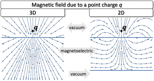
Graphical abstract
1. Introduction
Magnetoelectric media [Citation1–3] are characterized by unconventional equilibrium responses to an electric field and a magnetic field
. While
induces only an electric polarization
in ordinary materials, it also creates a magnetization
in magnetoelectrics. Similarly atypical is an electric polarization arising due to
in addition to a magnetization. The full range of linear electromagnetic responses occurring in a magnetoelectric material is embodied in the constitutive relations expressing the electric displacement field
and the field
in terms of
and
, which read
Here and
are the familiar [Citation4] materials tensors of electric permittivity and magnetic permeability, respectively. The magnetoelectric tensor
is associated with the magnetic-field-induced electric polarization, and its transpose
governs the electric-field-induced magnetization [Citation1–3]. The interested reader can find a more in-depth discussion of constitutive relations for magnetoelectrics in Appendix A, including a juxtaposition of two commonly adopted conventions.
Seminal works on the magnetoelectric effect were largely focused on the symmetry classification of materials with nonvanishing [Citation5,Citation6], but ramifications of magnetoelectric responses have also been discussed early on [Citation7]. However, it was the advent of multiferroic materials [Citation8,Citation9] with their large magnetoelectric couplings [Citation10–13] that has greatly boosted current interest in gaining a deeper understanding about magnetoelectricity [Citation14], also with the view to enable useful applications [Citation15–19]. The intriguing connection with the particle-physics concept of axion electrodynamics [Citation20–22] has recently become even more relevant through the realization of topological insulators [Citation23–27] and Weyl semimetals [Citation26–29]. The opportunity to explore sizable magnetoelectric effects in real materials has spurred efforts to describe unconventional electromagnetic phenomena exhibited by magnetoelectrics [Citation30–40]. Among these, simulations of magnetic-monopole fields have been paradigmatic [Citation30–32,Citation37,Citation39].
Nanostructuring generally opens up new avenues for controlling materials properties, including those of multiferroics and magnetoelectrics [Citation41,Citation42]. Recent advances in the design of two-dimensional (2D) atomic crystals [Citation43] and their versatile combination [Citation44–46] have transcended the original platform of low-dimensional systems created in semiconductor heterostructures [Citation47,Citation48]. With magnetic 2D materials already realized in metal [Citation49] and semiconductor quantum wells [Citation50] as well as atomic crystals [Citation51–54], the focus has shifted to the possibility of 2D multiferroics and magnetoelectrics [Citation52–58]. In this context, the purpose of this Review is two-fold. In Sec. 2, we present a survey of 2D materials where magnetoelectricity is expected and/or has already been observed. In the subsequent Sec. 3, we discuss the ramification of a 2D material’s finite size on its magnetoelectric responses, focusing especially on magnetic-monopole fields generated by electric charges placed near or in the medium. Our work is intended to raise awareness of the special features associated with magnetoelectricity in low-dimensional materials, which have been discussed only sporadically until now [Citation59].
2. Survey of 2D magnetoelectric materials
The systematic discussion of magnetoelectric materials properties is usually based on consideration of a medium’s free-energy density . Its expansion up to quadratic order in electric and magnetic field components is most generally given by [Citation2,Citation3]
Here and
are the material’s spontaneous electric polarization and magnetization, respectively, while
and
denote the conventional [Citation4] electric and magnetic susceptibility tensors. The linear magnetoelectric effect is embodied in the term containing
. Contributions to
giving rise to nonlinear electromagnetic (including higher-order magnetoelectric [Citation3,Citation60,Citation61]) responses have been omitted from EquationEq. (2
(2)
(2) ), as we are not focusing on these in the following. Similarly, possible interactions between simultaneously present spontaneous electric and magnetic orders, such as
being affected when switching
in multiferroics, are not being considered in the following unless these present a mechanism for generating a novanishing
.
General descriptions of materials properties in terms of tensor quantities can be obtained based on fundamental symmetry considerations [Citation62]. For example, magnetoelectricity can occur only in systems where both spatial-inversion and time-reversal symmetries are broken. This allows us to distinguish the magnetoelectric responses we are interested in from the superficially related phenomena of current-induced magnetization [Citation63] or spin-orbit torque [Citation64], which are based on a relation between the magnetization and an electric-current density
[Citation65–68]. If the current originates from an applied electric field and is related to the latter via Ohm’s law,
, the resulting dependence of the magnetization on the electric field,
looks similar to the magnetoelectric effect [Citation69]; see Eq. (A1b). However, the basic conditions for the tensor to exist in a material differ from those required for nonvanishing
. Most importantly, current-induced magnetization is possible in materials with unbroken time-reversal symmetry. Furthermore, in contrast to the magnetoelectric effect which is an equilibrium phenomenon, nonequilibrium mechanisms are crucial for generating a magnetization accompanying the electric current [Citation63]. Recent theoretical studies have explored current-induced magnetization in 2D materials, e.g. in twisted bilayer graphene [Citation70] and the interfacial 2D electron gas in SrTiO
[Citation71]. Spin-orbit torques in magnetic 2D materials, such as Fe
GeTe
[Citation72] and CrI
[Citation73] have also been considered. An intriguing realization of current-induced magnetization in the 2D transition-metal dichalcogenide MoS
[Citation74] utilized the material’s valley-isospin degree of freedom [Citation75].
We focus here only on magnetoelectric 2D materials, i.e. those having finite . To impose some order on the rapidly expanding zoo of 2D magnetoelectrics, materials are grouped into subsections according to the basic mechanisms underlying their magnetoelectric responses. We start by discussing 2D versions of single-phase magnetoelectrics and multiferroics in Sec. 2.1. Following that, Sec. 2.2 provides an overview of 2D multiferroic heterostructures. Sec. 2.3 is dedicated to magnetic 2D materials whose (ferro- or antiferro-)magnetic order is tunable by electric fields. The unconventional magnetoelectricity of 2D charge carriers in semiconductor quantum wells is considered in Sec. 2.4. We conclude the survey of 2D magnetoelectric materials with Sec. 2.5 exploring the ways in which the valley-degree of freedom enables magnetoelectric responses in 2D atomic crystals, such as few-layer sheets of graphene or transition-metal dichalcogenides.
2.1. Single-phase 2D magnetoelectrics
Before the advent of multiferroics, the typical magnetoelectric bulk material was expected to be an inversion-asymmetric time-reversal-breaking antiferromagnet, much like the first and paradigmatic example CrO
[Citation5,Citation76]. Although time-reversal symmetry is always broken in ferromagnets but not in all antiferromagnets [Citation77], inversion symmetry is rarely broken in ferromagnets unless the underlying crystal structure is already noncentrosymmetric. In contrast, antiferromagnetic order itself can break inversion symmetry, thus greatly multiplying the possibilities for realizing a magnetoelectric material. By now, many antiferromagnetic compounds are known to be magnetoelectric, but the magnitude of their magnetoelectric couplings
are usually small [Citation3] – the current record holder is TbPO
with
[Citation78,Citation79].
Despite the fact that the smallness of magnetoelectric couplings is generic for single-phase antiferromagnets, those among them that are van-der-Waals crystals can serve as an attractive starting point for fabricating 2D magnetoelectrics. Pertinent examples are MnPS [Citation80] and NiI
[Citation81], whose intralayer antiferromagnetic order has been shown to persist in the few-layer limit [Citation82–84]. To date, there has been no direct confirmation of the magnetoelectric effect in these 2D allotropes of bulk magnetoelectrics, but the presence of all necessary ingredients is promising and should motivate further exploration of these materials [Citation85] and similar candidates [Citation86,Citation87].
An interesting alternative to planar antiferromagnets is presented by layered magnets where the magnetization direction alternates between adjacent layers. Bilayers of such materials could constitute single-phase antiferromagnets and show the magnetoelectric effect. A prominent example is CrI for which the magnetoelectric coupling has been measured to be
[Citation88]. See also related experiments [Citation89,Citation90] and theoretical work [Citation91,Citation92]. It can be expected that similar materials such as WSe
and CrTe
also exhbibit magnetoelectricity [Citation92].
Single-phase materials with large magnetoelectric effects are typically multiferroic, i.e. exhibit coexisting spontaneous electric polarizations and magnetizations. There is, however, a paucity of such materials even in bulk, because the most effective mechanisms for generating ferromagnetisms and ferroelectricity are mutually exclusive [Citation93] due to a classic case of chemical contra-indication [Citation94]: ferroelectrics favor having empty d or f orbitals, whereas magnetism typically arises when these orbitals are partially filled. In fact, no 2D materials that are single-phase ferromagnetic-ferrolectric multiferroics have been realized so far [Citation58], but theoretical studies are pointing to a number of promising candidates: CrN and CrB [Citation95], MXene bilayers [Citation96], monolayer (CrBr
)
Li [Citation97], TMPCs-CuMP
X
[Citation98,Citation99], monolayer Hf
VC
F
[Citation100], monolayer VOCl
[Citation101] and VOI
[Citation102] (but see also Ref [Citation103]), halogen-intercalated phosphorene bilayers [Citation104], transition-metal-intercalated MoS
bilayers [Citation105], double-perovskite bilayers [Citation106], as well as monolayer
-In
Se
[Citation107].
2.2. 2D multiferroic heterostructures
Hybrid systems incorporating ferroelectric and ferromagnetic parts provide a promising avenue for overcoming the intrinsic limitations that make it so hard to have both a spontaneous electric polarization and a magnetization in the same material [Citation8]. In fact, gigantic magnetoelectric couplings of have recently been realized in the heterostructure multiferroic FeRh/BTO [Citation108]. The expectation that a similar strategy of combining 2D ferroelectrics with 2D ferromagnets will yield robust 2D multiferroics has fuelled intense theoretical efforts. We discuss below a number of promising materials combinations for which magnetoelectic phenomena in the wider sense have been predicted. However, the available theoretical results do not permit us to infer with certainty that the linear magnetoelectric effect occurs, or estimate the magnitude of magnetoelectric-tensor components
.
The first-considered van-der-Waals heterostructure of ferromagnetic CrGe
Te
combined with ferroelectric In
Se
showed intriguing properties [Citation109]. Besides demonstrating the ability to switch the magnetization of the Cr
Ge
Te
layer via reversal of the electric polarization in the In
Se
part, the latter became magnetized via the proximity effect – in effect becoming a single-phase 2D multiferroic.
The combination of magnetic bilayer CrI with ferroelectric monolayer Sc
CO
also yielded interesting magnetoelectric responses [Citation110]. Here the reversal of electric polarization in Sc
CO
triggered the transition between antiferromagnetic and ferromagnetic order in bilayer CrI
. The same mechanism for magnetoelectricity has also been studied theoretically for a bilayer-CrI
/monolayer-In
Se
multiferroic heterostructure [Citation111]. Even greater efficiency for electric control of the antiferromagnetic-to-ferromagnetic transition in bilayer CrI
is expected when it forms a van-der-Waals heterostructure with perovskite-oxide ferroelectrics such as BiFeO
[Citation112].
Control of the magnetization in FeGeTe
layers via the electric polarization of In
Se
was predicted to enable enhanced magnetotransport functionality in a tunnel-junction device [Citation113]. Transition-metal-decorated graphene can also be used as the magnetic part of a multiferroic heterostructure formed with monolayer In
Se
[Citation114].
2.3. 2D materials with electrically tunable spontaneous magnetization
Magnetic order generally arises from the exchange interaction between microscopic magnetic moments. In systems where the exchange-interaction strength depends on tunable electronic degrees of freedom, e.g. the charge density in a semiconductor [Citation50], the spontaneous magnetization can become a function of the applied electric field
. Electric control of magnetism based on such mechanisms is attracting a lot of interest [Citation115] but has typically not been discussed using the language and formalism of the magnetoelectric effect. Nevertheless, in the spirit of the expansion (Equation2
(2)
(2) ) for the field-dependent part of the system’s free-energy density, a term
actually incorporates magnetoelectricity with a tensor whose elements
quantify the electric-field tunability of the spontaneous magnetization. Typical magnitudes
have been realized in the dilute magnetic semiconductor GaMnAs [Citation116].
Magnetoelectric effects arising from an electric-field-dependent spontaneous magnetization have been discussed theoretically [Citation117,Citation118] and observed experimentally [Citation119,Citation120] in 2D quantum-well structures made from dilute-magnetic semiconductors. Few-layer CrGe
Te
has recently been shown to exhibit electric-field-tunable ferromagnetism [Citation121–123]. Using experimental data and results of calculations presented in Ref [Citation122], we estimate
for this 2D magnetoelectric material. It would be interesting to explore whether other currently available electrically tunable 2D magnets, e.g. monolayer Fe
GeTe
[Citation124], also exhibit the linear magnetoelectric effect.
2.4. Magnetoelectricity of 2D charge carriers in quantum wells
In bulk conductors, screening and nonequilibrium responses associated with the application of an electric field or the generation of an electric polarization generally preclude any discussion of the magnetoelectric effect.Footnote1 Low-dimensional conductors, however, can exhibit equilibrium responses as long as and
are parallel to spatial directions within which charge-carrier motion is quantized [Citation125–127]. Furthermore, 2D-conductor samples fitted with front and back gates allow changing of
at constant charge density [Citation128–131], thus making it possible to disentangle electric-polarization responses from charging effects in experiments. Conducting 2D materials are therefore ideally suited for a detailed exploration of magnetoelectricity associated with itinerant charge carriers. In this subsection, we focus on the paradigmatic example of 2D conductors realized in semiconductor-heterostructure quantum wells [Citation47]. A pedagogical introduction to the basic principles of band-gap engineering and physical properties of 2D semiconductor structures is available, e.g. in Ref [Citation48] (especially Chapter 4).
Figure 1. Mechanisms underpinning magnetoelectricity in semiconductor-heterostructure quantum wells. Charge carriers can move freely in the plane but are confined in
direction by a symmetric potential arising from the spatially varying conduction-band bottom (drawn in black pen). Equilibrium currents [(a)] and bound-state charge distributions [(b)] are indicated in red. The band bending shown schematically in the right panel of subfigure (a) is due to the applied perpendicular electric field. The qualitatively similar, but typically much smaller in magnitude, band bending arising as a consequence of the magnetic-field-induced electric polarization is not shown in the right panel of subfigure (b).
![Figure 1. Mechanisms underpinning magnetoelectricity in semiconductor-heterostructure quantum wells. Charge carriers can move freely in the xy plane but are confined in z direction by a symmetric potential arising from the spatially varying conduction-band bottom (drawn in black pen). Equilibrium currents [(a)] and bound-state charge distributions [(b)] are indicated in red. The band bending shown schematically in the right panel of subfigure (a) is due to the applied perpendicular electric field. The qualitatively similar, but typically much smaller in magnitude, band bending arising as a consequence of the magnetic-field-induced electric polarization is not shown in the right panel of subfigure (b).](/cms/asset/f15bee39-74a0-473c-8bd6-305439237892/tapx_a_2032343_f0001_oc.jpg)
The microscopic origin of magnetoelectricity in quantum wells are quadrupolar equilibrium currents whose distortion by an applied electric field generates a magnetization [Citation132]. Such equilibrium-current distributions arise from the interplay of spatial-inversion asymmetry with an applied magnetic field [Citation132,Citation133], or with an intrinsic exchange field due to ferromagnetic order [Citation132,Citation133], or with the staggered exchange field of a nontrivial antiferromagnetic order [Citation132].Footnote2 Furthermore, an applied magnetic field shifts the 2D-bound-state charge distribution, thus inducing an electric polarization perpendicular to the well [Citation132,Citation133], as mandated by the duality of magnetoelectric reponses [Citation1,Citation2]. illustrates schematically the microscopic mechanisms for magnetoelectric responses in semiconductor-heterostructure quantum wells. According to theoretical estimates [Citation132], the magnitude of the magnetoelectric-tensor components in quantum wells can reach values , and the
-induced magnetic moment per 2D charge carrier can be as large as
Bohr magnetons.
2.5. Magnetoelectricity in 2D materials from topology or valley isospin
Exotic types of magnetoelectricity have been suggested to exist in certain materials, even those in which time-reversal and spatial-inversion symmetries are not broken. One example for these are topological insulators [Citation23–27], which have an isotropic magnetoelectric coupling with a quantized magnitude
. Among the multitude of 2D materials, a topological magnetoelectric effect was predicted [Citation134–136], and its signatures have recently been observed [Citation137,Citation138], in even-layer MnBi
Te
.Footnote3 While interesting from a fundamental point of view, the inability to adjust the magnitude of the topological magnetoelectric coupling limits its relevance for applications – unless proposals for engineering tunable magnetoelectric couplings via symmetry-breaking finite-size effects in thin MnBi
Te
layers [Citation139] come to fruition.
Materials with a valley-isospin degree of freedom [Citation75] lend themselves to an intriguing realization of electrically tunable magnetoelectricity. Concrete proposals for 2D materials have been formulated for bilayer graphene [Citation140,Citation141] and transition-metal-dichalcogenide bilayers [Citation142]. In all these cases, electronic states from different valleys in the 2D-material band structure (usually labelled and
) are connected via time reversal or spatial inversion. An imbalance between charge-carrier densities in the two valleys – a finite valley-isospin density – amounts to a breaking of both symmetries [Citation127] and renders the material magnetoelectric. As various ways for addressing valley isospin have been explored as part of a drive to realize electronic devices based on a new valleytronics paradigm [Citation143], these systems offer the unique opportunity for generating electrically tailored magnetoelectric couplings.
3. Electromagnetism of 2D magnetoelectric media
The survey of 2D magnetoelectric media presented in the previous section outlines the great progress being made in designing, fabricating and characterizing such materials. Once the remaining materials-science challenges are overcome, the focus of further investigations will shift to exploring more broadly how such materials behave electromagnetically. In anticipation of that, this section focuses on a paradigmatic property of magnetoelectric media: the simulation of magnetic-monopole fields discussed extensively for bulk systems [Citation30–32,Citation37]. Below we briefly describe how isotropic magnetoelectric responses can be included as unconventional source terms into the Maxwell equations of ordinary electrodynamics, thus mimicking the effects of axion electrodynamics [Citation20–23]. This forms the basis for solving boundary-value problems involving isotropic magnetoelectrics and enables a generalization of the well-known method of images [Citation4] to include image magnetic monopoles alongside image charges [Citation30]. In the following, we refer to this approach as the method of image dyons and use it to obtain electric and magnetic fields generated by an electric charge placed near or in a finite-width magnetoelectric slab.
A configuration of external sources (i.e. electric charges and currents) determines the electromagnetic fields via the inhomogeneous Maxwell equations [Citation4]
Here and
denote the charge and current densities, respectively, as a function of position
, and
is the gradient operator. Solving (Equation4
(4)
(4) ), in conjunction with the set of homogeneous Maxwell equations
and the constitutive relations (Equation1(1)
(1) ) that embody the effect of microscopic degrees of freedom in media, yields the fields throughout space.
As a starting point for exploring the interplay between low dimensionality and magnetoelectricity, we focus in the following on the case of media with isotropic magnetoelectric response whose magnetoelectric tensor has the form . For consistency, isotropy is also assumed for the ordinary polarization and magnetization responses, i.e.
and
. To make modifications arising from isotropic magnetoelectricity more explicit, the field-source relations (Equation4
(4)
(4) ) can be rewritten as
The particular form of the inhomogeneous Maxwell equations given in (Equation6(6)
(6) ) coincides with the one derived in the context of axion electrodynamics [Citation20,Citation21] whose realization in condensed-matter systems is currently attracting great interest [Citation26,Citation27]. It shows that, in situations with piecewise-constant
, e.g. when certain parts of space are filled with a homogeneous isotropic magnetoelectric medium, the effects of magnetoelectricity can be represented in terms of charges and currents induced at interfaces.
Various theoretical techniques have been used to solve the set of equations describing electromagnetisms with magnetoelectric media [Citation30–35]. Below we discuss in greater detail the method of introducing image charges and monopoles [Citation30] to satisfy boundary conditions of electromagnetic fields at an interface between vacuum and an isotropic magnetoelectric medium. Generalizing this approach to the case with more than a single interface enables us to investigate how the finite width of a 2D magnetoelectric medium affects its unconventional electromagnetism.
3.1. Image dyons for solving boundary-value problems in magnetoelectrics
The method of image charges is an established technique for solving boundary-value problems in electrostatics [Citation4]. It is based on the possibility to use an appropriately placed fictitious (i.e. image) point charge to represent the polarization-charge distribution generated at an interface by the presence of a real electric point charge. This approach turns out to be most useful when considering high-symmetry configurations, e.g. when the real charges are placed in spaces with planar, cylindrical or spherical interfaces between different media. In particular, the image-charge method has been applied to obtain the electric fields generated by a charge near [Citation144] or inside [Citation145] a dielectric plate.
Figure 2. An electric charge placed near a planar interface (located at
) between an ordinary dielectric (occupying the region
) and a magnetoelectric medium (present in region
) generates image dyons on both sides. The values of their electric (magnetic) charges are related via
(
).
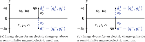
The method of image charges can be extended to describe situations involving magnetoelectrics by allowing magnetic monopoles [Citation146] alongside each of the electric image charges [Citation30], thus effectively rendering the image objects to be dyons [Citation147,Citation148]. See for an illustration of the previously considered case of an electric charge near a single planar boundary between vacuum and a magnetoelectric medium [Citation30,Citation32,Citation149]. Below we juxtapose the known results for this case with those calculated for our situation of interest, which is a charge placed near or inside a finite-width slab of magnetoelectric material. Analogous to the situation of an electric point charge near or inside a dielectric plate where an infinite number of image charges need to be considered [Citation144,Citation145], an infinite number of image dyons are required for describing the finite-slab magnetoelectric. shows the configurational details pertaining to this case. Before presenting our results, we briefly state the boundary-value problem posed by planar interfaces with magnetoelectric media and sketch the formalism underpinning the image-dyon method used for its solution.
Figure 3. An infinite set of image dyons is needed to describe electric and magnetic fields generated by an electric point charge
placed near [panel (a)] or inside [panel (b)] a finite-width slab of magnetoelectric material. Here
labels dyons arising from mirror-imaging at the upper (lower) boundary,
when the image dyon is located above (below) the
boundary, and
is a counter associated with the dyon location. Dyons with
arise only for the case with
inside the magnetoelectric medium [panel (b)].
![Figure 3. An infinite set of image dyons dkmν is needed to describe electric and magnetic fields generated by an electric point charge q0 placed near [panel (a)] or inside [panel (b)] a finite-width slab of magnetoelectric material. Here m=U(L) labels dyons arising from mirror-imaging at the upper (lower) boundary, ν=+(−) when the image dyon is located above (below) the m boundary, and k∈Z∖0 is a counter associated with the dyon location. Dyons with k<0 arise only for the case with q0 inside the magnetoelectric medium [panel (b)].](/cms/asset/50ea46fd-ddf2-4744-883d-fda2835c401d/tapx_a_2032343_f0003_oc.jpg)
Considering the static limit and assuming any field sources entering the r.h.s. of the inhomogeneous Maxwell equationsEquation(4)(4)
(4) to be localized away from a planar interface that is parallel to the
plane and intersects the
axis at
, the electromagnetic fields obey the boundary conditions
Here cylindrical coordinates are utilized for positions, and
. Furthermore, the static limit enables both the electric field and the magnetic field to be expressed in terms of scalar potentials,
The method of image dyons amounts to writing Ansätze for the scalar potentials arising in a given region of space, due to having a source charge at the location
, in terms of a superposition of electric-point-charge and magnetic-monopole contributions,
Here (
) denote the electric (magnetic) charge of the fictitious image dyon
located at
. It is understood that the sum
is restricted to include only those image dyons that are relevant for calculating the fields in a given region, i.e. those that are located outside. Furthermore,
(
) is the permittivity (permeability) of the region where the source charge is located. To begin with, the electric and magnetic charges making up each image dyon
as well as its location
are unknown. However, the location
can be predicted based on the geometry of the system if we require it to be independent of the charges
and
. It turns out that
is the location of first- or higher-order mirror images of the source charge with respect to the boundary (or boundaries). Since the slab geometry considered in this work has planes perpendicular to the
axis as its boundaries, and since we assume that the electric source charge is located at
with
, the locations of the image dyons are
with the coordinate
determined by
and the slab width
. In particular, if the magnetoelectric medium is semi-infinite (i.e. there is only one boundary, assumed to be located at
without loss of generality), we only have two image dyons
and
as shown in , and EquationEq. (9)
(9)
(9) simplifies. Furthermore, we find the relations
and
. Full details of the calculation and results for image-dyon charges are given in Appendix B.1.
If the magnetoelectric medium has the shape of a finite-width slab, an infinite number of image dyons exists as shown in . We can see this by trying to satisfy the field-continuity conditions for each of the two boundaries in turn. Assuming the source charge to be outside the slab, we can start by satisfying the upper boundary conditions while ignoring the lower boundary – this yields the image dyons
at
and
at
as in the single-interface situation depicted in ). [Here and in the following, the superscript U(L) is used to indicate that the image dyon results from mirroring at the upper (lower) boundary, which is at
(
), the
(
) label next to it specifies that the charge is located above (below) that boundary, and the integer
relates to the image-dyon location as explained below.] Attempting next to satisfy the boundary conditions at the bottom interface while ignoring the upper boundary, we treat the dyon
at
as the source and obtain additional image dyons
at
and
at
. However, their introduction causes boundary conditions at the upper interface to no longer be satisfied. To remedy this, two more image dyons need to be created;
at
and
at
, whose properties are determined from assuming dyon
as the source. This in turn causes boundary conditions at the lower interface to be violated, which needs to be fixed by further iteration of the image-dyon method. In the end, an infinite number of image dyons are needed to satisfy the boundary conditions at both interfaces asymptotically.
For the case when the source charge is inside the slab, even more image dyons are needed as shown in ). Similar as before, we can start by satisfying the upper boundary conditions while ignoring the lower boundary, and obtain image dyons
at
and
at
. Next, we satisfy the lower boundary conditions while ignoring the upper boundary and obtain
at
,
at
,
at
, and
at
by treating both
and the dyon
as sources. The subset of these image dyons having
are equivalent to the image dyons found for the case with the source charge outside the slab, and further iteration builds up the same structure as shown in ). In contrast, the subset of image dyons labelled by
are entirely new, and their subsequent alternate mirroring creates infinitely many additional dyons.
Generally, the location of an image dyon is at
Similar to the case where the magnetoelectric medium is semi-infinite, we have and
. The general formulae for calculating the image-dyon charges in the above mentioned iterating process are derived in Appendix B.1.2, and the results are given in Appendix B.2. Note that the relevant image dyons for determining electromagnetic fields in different regions are different. The fields present in the part of space
(
) are equivalent to those created by the source charge and image dyons
(
). The field inside the medium is equivalent to that created by the source charge and the image dyons
and
. By superposing the fields generated by the source charge and all relevant image dyons and taking the asymptotic limit, we can obtain the field configurations in different regions.
The general principles of the image-dyon method and its detailed results can also be formally obtained by rewriting EquationEq. (9)(9)
(9) using the geometry-adapted Sommerfeld-type identity [Citation150–152]
where . Due to cylindrical symmetry with respect to the
axis, we can focus on calculating the scalar potentials in one of the planes including
axis and then extend the results to other planes by rotation. Thus assuming
in cylindrical coordinates, and for
, we find
After determining the initially unknown coefficients via the boundary conditions,
(
) can be interpreted in terms of electric charges
(magnetic charges
) and their locations
. Furthermore,
(
) in the region above (below) the slab since we require scalar potentials to vanish at infinity. Thus the image-dyon representation is obtained via EquationEq. (11)
(11)
(11) .
3.2. Fields from a point charge placed in or near a magnetoelectric plate
Without loss of generality, we assume a positively charged point source () from now on and only calculate electromagnetic fields in the plane
. As a basic illustration of the magnetoelectric effect, we first present results for an artificial situation where the magnetoelectric has the same dielectric constant
and magnetic permeability
as the surrounding medium; i.e. the magnetoelectric medium only differs by having finite
. Fields for configurations with these parameter values and the electric source charge located near (inside) the magnetoelectric are shown in (). Results for a more realistic set of magnetoelectric-medium parameters (
,
,
) are shown in . To provide further insight into the obtained field configurations, we indicate the locations of maxima in the distributions of interfacial currents and charges. Plots of the interface-current distributions in finite-width slab geometries are shown in .
Figure 4. Field lines of the electric () and magnetic (
) fields generated by an electric point charge located outside an isotropic magnetoelectric medium occupying the space
and having the same dielectric constant and magnetic permeability as the surrounding ordinary medium (
,
). The black dot indicates the location of the source charge, and horizontal thick blue lines delineate interfaces between ordinary and magnetoelectric media. Green circles are positioned where the interface-current distribution has maxima and show the current direction. Yellow circles are positioned where the interface-charge distribution has maxima and show its sign. The magnetoelectric is assumed to have
.
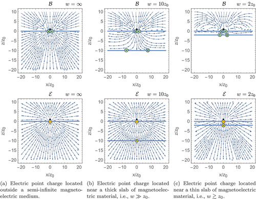
Figure 5. Field lines of the electric () and magnetic (
) fields generated by an electric point charge located inside an isotropic magnetoelectric medium occupying the space
and having the same dielectric constant and magnetic permeability as the surrounding ordinary medium (
,
). The black dot indicates the location of the source charge, and horizontal thick blue lines delineate interfaces between ordinary and magnetoelectric media. Green circles are positioned where the interface-current distribution has maxima and show the current direction. Yellow circles are positioned where the interface-charge distribution has maxima and show its sign. The magnetoelectric is assumed to have
.
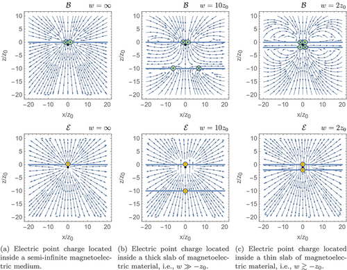
Figure 6. Field lines of the electric () and magnetic (
) fields generated by an electric point charge located outside an isotropic magnetoelectric medium occupying the space
and having
,
, and
. The black dot indicates the location of the source charge, and horizontal thick blue lines delineate interfaces between ordinary and magnetoelectric media. Green circles are positioned where the interface-current distribution has maxima and show the current direction. Yellow circles are positioned where the interface-charge distribution has maxima and show its sign.
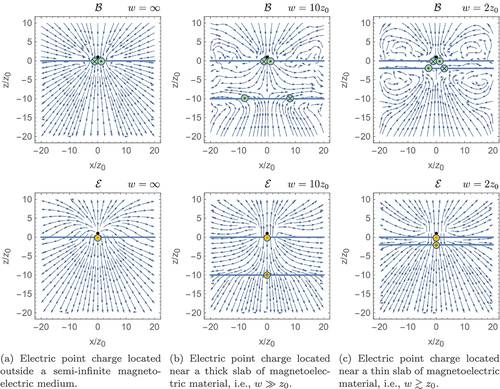
Figure 7. Magnetoelectrically induced interface currents in the slab geometries considered in this work. The blue (yellow) curves show the variation of the current-density component at the upper (lower) boundary as a function of coordinate
. Pairs
of values associated with positive-current maxima are indicated, allowing also the negative-current maxima to be identified via symmetry as
. Panel (a) [(b), (c), (d), (e), (f)] pertains to the situations shown in ) [), ), ), ), )].
![Figure 7. Magnetoelectrically induced interface currents in the slab geometries considered in this work. The blue (yellow) curves show the variation of the current-density component Jy at the upper (lower) boundary as a function of coordinate x/z0. Pairs (x/z0,Jy) of values associated with positive-current maxima are indicated, allowing also the negative-current maxima to be identified via symmetry as (−x/z0,−Jy). Panel (a) [(b), (c), (d), (e), (f)] pertains to the situations shown in Figure 4(b) [Figure 6(b), Figure 5(b), Figure 4(c), Figure 6(c), Figure 5(c)].](/cms/asset/d06bf10e-43dc-4f32-b573-7e9f00978045/tapx_a_2032343_f0007_oc.jpg)
We start by discussing the idealized situation with and
, i.e. when the differentiating characteristic of the region inside (outside) the magnetoelectric medium is a finite (vanishing)
. When the entire half-space
is occupied by the magnetoelectric, there is only one boundary in the system, on which the surface currents and surface charges are induced by the source electric charge, as indicated in ) and . Since the image charges are effective representations of the surface currents and surface charges, the two magnetic image monopoles
and
located at different sides of the boundary have the same magnitudes but opposite signs while the two electric image charges
and
are identical. Therefore, when
and
, the magnetic field above the boundary is non-zero and mirror-symmetric to the one below but with opposite directions. The electric field, specifically
, is not continuous across the boundary, which is a result of the superposition of the electric field generated by the real source charge and the one generated by the electric image charges, with the latter ones being symmetric with respect to the boundary. When the width
of the magnetoelectric medium is finite and the source charge placed above it, the magnetic fields are non-zero above and inside the slab but vanish below, as shown in ) and . The vanishing of the magnetic field below the slab is due to the cancellation effect between the magnetic fields generated by the surface currents on the upper and lower boundaries since the directions of the induced currents are opposite at the two boundaries. Furthermore, the magnitude of the current density at the lower surface is weaker than the one at the upper surface since the lower boundary is further away from the source charge and is more spread out, as can be seen from . The electric field has the same form inside and below the slab, which arises due to the boundary conditions at
where
. As the slab width
decreases, the magnetic field more and more resembles the one generated by a magnetic quadrupole, especially when the source charge is located inside the magnetoelectric medium [see )]. This is because the distributions of the surface currents in terms of their magnitudes at the two boundaries become more and more similar as the slab becomes thinner (see ). Therefore, we expect the magnetic field to be the same as a quadrupole field when the slab is effectively 2D since the upper and lower surface current will generate the same but opposite magnetic dipole moments.
Real materials typically have a dielectric constant that is much larger than that of vacuum (
) and quite small values of
measured in units of
. For example, in the paradigmatic magnetoelectric Cr
O
,
,
, and
[Citation22].Footnote4 We present results for such a materials combination in . In the previously discussed case with
, induced charges and currents at the interfaces arose entirely as a result of magnetoelectricity, i.e. the piecewise-constant spatial variation of
[see EquationEq. (6)
(6)
(6) ]. Due to the additional variation in
between the ordinary and magnetoelectric media, there will be an extra electric response. Due to the magnetoelectric effect, this extra electric response leads to an extra contribution to the interface current at the lower boundary. As a result, the magnetic field no longer vanishes in the region below the slab. It rather resembles the magnetic field above the medium, especially when the slab is thin, as illustrated in .
illustrates in greater detail parametric dependencies of the dipolar interface-current distributions that are induced magnetoelectrically by an electric source charge in slab geometries. The presented results are calculated brute-force by taking . The upper (lower) row of plots is associated with the thick (thin) slabs, with plots paired in the same column pertaining to the same source-charge location and the same material combination. The line shapes rationalize the observed quadrupolar patterns of magnetic field lines, especially in the thin-slab limit.
4. Conclusions
We have reviewed the currently available variety of theoretically proposed and experimentally realized 2D magnetoelectric materials. Both the already well-established 2D-quantum-well systems in semiconductor heterostructures and the more recently fabricated 2D atomic crystals are viable platforms for the detailed exploration and possible device application of magnetoelectricity. At present, however, theoretical proposals vastly outnumber actual experimental realizations. Thus a concerted effort is needed to pursue the promising theoretical leads and overcome basic materials challenges.
Where experimental data are available, we have quoted or estimated the magnitudes of magnetoelectric couplings in 2D materials. Sizable values have been demonstrated for bilayer CrI, but most other measurements are indicative of much weaker magnetoelectricity than is typically exhibited in single-phase bulk magnetoelectrics. We expect that significantly larger magnetoelectric coupling should be observed in 2D multiferroic heterostructures, but these materials still need to be realized.
In addition to the survey of materials, we also discussed the implications of low dimensionality for paradigmatic magnetoelectric responses, focusing specifically on magnetic-monopole fields generated by electric charges near or in magnetoelectric media. To solve the associated boundary-value problem, we employed a generalization of the classical image-charge method where images carry both electric and magnetic charges, thus forming image dyons. Previously applied only to treat a single interface between an ordinary material and a magnetoelectric, we extended the formalism to describe a magnetoelectric plate. Finite-size effects are shown to importantly affect the magnetoelectric responses. These results provide a useful guide for further experimental exploration of magnetoelectricity in 2D materials, and they will hopefully stimulate broader investigation of this interesting current topic.
Disclosure statement
No potential conflict of interest was reported by the author(s).
Correction Statement
This article has been corrected with minor changes. These changes do not impact the academic content of the article.
Additional information
Funding
Notes
1. Despite being sometimes loosely linked with magnetoelectricity, the current-induced magnetization [Citation63] that is possible in gyrotropic conductors and the chiral magnetic effect exhibited by Weyl semimetals [Citation28,Citation29] are fundamentally different from the equilibrium-magnetoelectric responses focused on here.
2. The first scenario where the application of a magnetic field causes the quadrupolar equilibrium currents that are the basis for magnetoelectricity technically constitutes a field-induced (i.e. higher-order) magnetoelectric effect [Citation60,Citation132]. Note also that the mechanism for magnetoelectricity to occur via equilibrium quadrupolar currents in a ferromagnetic-semiconductor quantum well is fundamentally different from the magnetoelectric response arising from the charge-density tunability of the spontaneous magnetization discussed in Sec. 2.3.
3. To be precise, even-layer MnBiTe
is actually antiferromagnetic and therefore not a time-reversal-invariant topological insulator but an axion insulator [Citation27]. This distinction matters because the fate of axion electrodynamics in the 2D limit of nonmagnetic topological-insulator slab geometries is rather intricate [Citation25].
4. Strictly speaking, the magnetoelectric response of CrO
is not isotropic but uniaxial, i.e. described by a tensor
with
[Citation155–157]. In our model for a realistic isotropic magnetoelectric, we use the value of
[Citation22].
References
- O’Dell TH. The electrodynamics of magneto-electric media. Amsterdam: North-Holland; 1970.
- Landau LD, Lifshitz EM. Electrodynamics of continuous media. Second Revised ed. Oxford: Pergamon; 1984.
- Fiebig M. Revival of the magnetoelectric effect. J Phys D. 2005;38:R123.
- Jackson JD. Classical electrodynamics. 3rd ed. New York (NY): Wiley; 1999.
- Dzyaloshinski IE. On the magneto-electrical effect in antiferromagnets. Zh Eksp Teor Fiz. 1959;37:881–33. [Sov Phys JETP, 628.:. 1960.
- Schmid H. On a magnetoelectric classification of materials. Int J Magn. 1973;4:337–361.
- Siratori K. Magneto-electric effect and solid state physics. Ferroelectrics. 1994;161:29–41.
- Fiebig M, Lottermoser T, Meier D, et al. The evolution of multiferroics. Nat Rev Mater. 2016;1:16046.
- Spaldin NA. Multiferroics: past, present, and future. MRS Bull. 2017;42:385–390.
- Eerenstein W, Mathur ND, Scott JF. Multiferroic and magnetoelectric materials. Nature. 2006;442:759–765.
- Dong S, Liu JM, Cheong SW, et al. Multiferroic materials and magnetoelectric physics: symmetry, entanglement, excitation, and topology. Adv Phys. 2015;64:519–626.
- Spaldin NA, Ramesh R. Advances in magnetoelectric multiferroics. Nat Mater. 2019;18:203–212.
- Dong S, Xiang H, Dagotto E. Magnetoelectricity in multiferroics: a theoretical perspective. Natl Sci Rev. 2019;6:629–641.
- Hu JM, Duan CG, Nan CW, et al. Understanding and designing magnetoelectric heterostructures guided by computation: progresses, remaining questions, and perspectives. npj Comput Mater. 2017;3:1–21.
- Chu YH, Martin LW, Holcomb MB, et al. Controlling magnetism with multiferroics. Mater Today. 2007;10:16–23.
- Fusil S, Garcia V, Barthélémy A, et al. Magnetoelectric devices for spintronics. Annu Rev Mater Res. 2014;44:91–116.
- Ortega N, Kumar A, Scott JF, et al. Multifunctional magnetoelectric materials for device applications. J Phys: Condens Matter. 2015;27:504002.
- Song C, Cui B, Li F, et al. Recent progress in voltage control of magnetism: materials, mechanisms, and performance. Prog Mater Sci. 2017;87:33–82.
- Manipatruni S, Nikonov DE, Lin CC, et al. Scalable energy-efficient magnetoelectric spin–orbit logic. Nature. 2019;565:35–42.
- Sikivie P. Experimental tests of the “invisible” axion. Phys Rev Lett. 1983;51:1415–1417.
- Wilczek F. Two applications of axion electrodynamics. Phys Rev Lett. 1987;58:1799–1802.
- Hehl FW, Obukhov YN, Rivera JP, et al. Relativistic nature of a magnetoelectric modulus of Cr2O3 crystals: a four-dimensional pseudoscalar and its measurement. Phys Rev A. 2008;77:022106.
- Qi XL, Hughes TL, Zhang SC. Topological field theory of time-reversal invariant insulators. Phys Rev B. 2008;78:195424.
- Essin AM, Moore JE, Vanderbilt D. Magnetoelectric polarizability and axion electrodynamics in crystalline insulators. Phys Rev Lett. 2009;102:146805.
- Armitage NP, Wu L. On the matter of topological insulators as magnetoelectrics. SciPost Phys. 2019;6:46.
- Nenno DM, Garcia CAC, Gooth J, et al. Axion physics in condensed-matter systems. Nat Rev Phys. 2020;2:682–696.
- Sekine A, Nomura K. Axion electrodynamics in topological materials. J Appl Phys. 2021;129:141101.
- Ma J, Pesin DA. Chiral magnetic effect and natural optical activity in metals with or without Weyl points. Phys Rev B. 2015;92:235205.
- Deng K, Van Dyke JS, Minic D, et al. Exploring self-consistency of the equations of axion electrodynamics in Weyl semimetals. Phys Rev B. 2021;104:075202.
- Qi XL, Li R, Zang J, et al. Inducing a magnetic monopole with topological surface states. Science. 2009;323:1184–1187.
- Fechner M, Spaldin NA, Dzyaloshinskii IE. Magnetic field generated by a charge in a uniaxial magnetoelectric material. Phys Rev B. 2014;89:184415.
- Meier QN, Fechner M, Nozaki T, et al. Search for the magnetic monopole at a magnetoelectric surface. Phys Rev X. 2019;9:011011.
- Martn-Ruiz A, Cambiaso M, Urrutia LF. Electro- and magnetostatics of topological insulators as modeled by planar, spherical, and cylindrical θ boundaries: green’s function approach. Phys Rev D. 2016;93:045022.
- Martín-Ruiz A, Cambiaso M, Urrutia LF. Axion electrodynamics in magnetoelectric media. In: Kamenetskii E, editor. Chirality, magnetism and magnetoelectricity. (topics in applied physics. Vol. 138. Cham: Springer; 2021. p. 459–492.
- Ouellet J, Bogorad Z. Solutions to axion electrodynamics in various geometries. Phys Rev D. 2019;99:055010.
- Ochiai T. Theory of light scattering in axion electrodynamics. J Phys Soc Jpn. 2012;81:094401.
- Khomskii DI. Magnetic monopoles and unusual dynamics of magnetoelectrics. Nat Commun. 2014;5:4793.
- Khomskii DI. Multiferroics and beyond: electric properties of different magnetic textures. J Exp Theor Phys. 2021;132:482–492.
- Uri A, Kim Y, Bagani K, et al. Nanoscale imaging of equilibrium quantum Hall edge currents and of the magnetic monopole response in graphene. Nat Phys. 2020;16:164–170.
- Kamenetskii EO. Electrodynamics of magnetoelectric media and magnetoelectric fields. Ann Phys. 2020;532:1900423.
- Velev JP, Jaswal SS, Tsymbal EY. Multi-ferroic and magnetoelectric materials and interfaces. Phil Trans R Soc A. 2011;369:3069–3097.
- Hu JM, Nan T, Sun NX, et al. Multiferroic magnetoelectric nanostructures for novel device applications. MRS Bull. 2015;40:728–735.
- Novoselov KS, Jiang D, Schedin F, et al. Two-dimensional atomic crystals. Proc Natl Acad Sci USA. 2005;102:10451–10453.
- Novoselov KS, Mishchenko A, Carvalho A, et al. 2D materials and van der Waals heterostructures. Science. 2016;353:aac9439.
- Liu Y, Weiss NO, Duan X, et al. Van der Waals heterostructures and devices. Nat Rev Mater. 2016;1:1–17.
- Sierra JF, Fabian J, Kawakami RK, et al. Van der Waals heterostructures for spintronics and opto-spintronics. Nat Nanotechnol. 2021;16:856–868.
- Bauer G, Kuchar F, and Heinrich H, editors. . In: Two-dimensional systems, heterostructures, and superlattices. Vol. 53 Springer series in solid-state sciences . Berlin: Springer; 1984.
- Davies JH. The physics of low-dimensional semiconductors. Cambridge (UK): Cambridge U Press; 1998.
- Himpsel FJ. Magnetic quantum wells. J Phys: Condens Matter. 1999;11:9483–9494.
- Dietl T, Ohno H. Dilute ferromagnetic semiconductors: physics and spintronic structures. Rev Mod Phys. 2014;86:187–251.
- Gibertini M, Koperski M, Morpurgo AF, et al. Magnetic 2D materials and heterostructures. Nat Nanotechnol. 2019;14:408–419.
- Gong C, Zhang X. Two-dimensional magnetic crystals and emergent heterostructure devices. Science. 2019;363:eaav4450.
- Mak KF, Shan J, and Ralph DC. Probing and controlling magnetic states in 2D layered magnetic materials. Nat Rev Phys. 2019 1 ;646–661.
- Wei S, Liao X, Wang C, et al. Emerging intrinsic magnetism in two-dimensional materials: theory and applications. 2D Mater. 2020;8:012005.
- Lu C, Wu M, Lin L, et al. Single-phase multiferroics: new materials, phenomena, and physics. Natl Sci Rev. 2019;6:653–668.
- Tang X, Kou L. Two-dimensional ferroics and multiferroics: platforms for new physics and applications. J Phys Chem Lett. 2019;10:6634–6649.
- Zhong T, Li X, Wu M, et al. Room-temperature multiferroicity and diversified magnetoelectric couplings in 2D materials. Natl Sci Rev. 2020;7:373–380.
- Gao Y, Gao M, Lu Y. Two-dimensional multiferroics. Nanoscale. 2021;13:19324–19340.
- Pournaghavi N, Pertsova A, MacDonald AH, et al. Nonlocal sidewall response and deviation from exact quantization of the topological magnetoelectric effect in axion-insulator thin films. Phys Rev B. 2021;104:L201102.
- Ascher E. Higher-order magneto-electric effects. Phil Mag. 1968;17:149–157.
- Grimmer H. The forms of tensors describing magnetic, electric and toroidal properties. Ferroelectrics. 1994;161:181–189.
- Nye JF. Physical properties of crystals. Oxford: Oxford University Press; 1957.
- Ganichev SD, Trushin M, Schliemann J. Spin polarization by current.In: Tsymbal EY, Žutić I, editors. Spintronics handbook: spin transport and magnetism. 2nd. Vol. 2, Chapter 7. Boca Raton: CRC Press; 2019. p. 317–338
- Manchon A, Železný J, Miron IM, et al. Current-induced spin-orbit torques in ferromagnetic and antiferromagnetic systems. Rev Mod Phys. 2019;91:035004.
- Ivchenko EL, Pikus GE. New photogalvanic effect in gyrotropic crystals. Pis’ma Zh Eksp Teo Fiz. 1978;27:640–643.[ JETP Lett. 27, 604 (1978)].
- Belinicher VI. Space-oscillating photocurrent in crystals without symmetry center. Phys Lett A. 1978 May;66:213–214.
- Aronov AG, Lyanda-Geller YB, Pikus GE. Spin polarization of electrons by an electric current. Sov Phys JETP. 1991;73:537–541.
- Edelstein VM. Spin polarization of conduction electrons induced by electron current in two-dimensional asymmetric electron systems. Solid State Commun. 1990;73:233–235.
- Levitov LS, Nazarov YV, Éliashberg GM. Magnetoelectric effects in conductors with mirror isomer symmetry. Zh Eksp Teor Fiz. 1985;88:229–236. [Sov. Phys. JETP 61, 133 (1985)]
- He WY, Goldhaber-Gordon D, Law KT. Giant orbital magnetoelectric effect and current-induced magnetization switching in twisted bilayer graphene. Nat Commun. 2020;11:1650.
- Johansson A, Göbel B, Henk J, et al. Spin and orbital Edelstein effects in a two-dimensional electron gas: theory and application to SrTiO3 interfaces. Phys Rev Res. 2021;3:013275.
- Johansen O, Risinggård V, Sudbø A, et al. Current Control of Magnetism in Two-Dimensional Fe3GeTe2. Phys Rev Lett. 2019;122:217203.
- Xue F, and Haney PM. Intrinsic staggered spin-orbit torque for the electrical control of antiferromagnets: Application to CrI3 Phys Rev B ; 2021 104 224414 . :
- Lee J, Wang Z, Xie H, et al. Valley magnetoelectricity in single-layer MoS2. Nat Mater. 2017;16:887–891.
- Xu X, Yao W, Xiao D, et al. Spin and pseudospins in layered transition metal dichalcogenides. Nat Phys. 2014;10:343–350.
- Rado GT. Statistical theory of magnetoelectric effects in antiferromagnetics. Phys Rev. 1962;128:2546–2556.
- Tinkham M. Group theory and quantum mechanics. New York: McGraw-Hill; 1964.
- Rado GT, Ferrari JM, Maisch WG. Magnetoelectric susceptibility and magnetic symmetry of magnetoelectrically annealed TbPO4. Phys Rev B. 1984;29:4041–4048.
- Rivera JP. A short review of the magnetoelectric effect and related experimental techniques on single phase (multi-) ferroics. Eur Phys J B. 2009;71:299.
- Ressouche E, Loire M, Simonet V, et al. Magnetoelectric MnPS3 as a candidate for ferrotoroidicity. Phys Rev B. 2010;82:100408.
- Kurumaji T, Seki S, Ishiwata S, et al. Magnetoelectric responses induced by domain rearrangement and spin structural change in triangular-lattice helimagnets NiI2 and CoI2. Phys Rev B. 2013;87:014429.
- Chu H, Roh CJ, Island JO, et al. Linear magnetoelectric phase in Ultrathin MnPS3 probed by optical second harmonic generation. Phys Rev Lett. 2020;124:027601.
- Long G, Henck H, Gibertini M, et al. Persistence of magnetism in atomically thin MnPS3 crystals. Nano Lett. 2020;20:2452–2459.
- Ju H, Lee Y, Kim KT, et al. Possible persistence of multiferroic order down to bilayer limit of van der Waals material NiI2. Nano Lett. 2021;21:5126–5132.
- Ni Z, Haglund AV, Wang H, et al. Imaging the Néel vector switching in the monolayer antiferromagnet MnPSe3 with strain-controlled Ising order. Nat Nanotechnol. 2021;16:782–787.
- Chittari BL, Park Y, Lee D, et al. Electronic and magnetic properties of single-layer MPX3 metal phosphorous trichalcogenides. Phys Rev B. 2016;94:184428.
- McGuire MA. Cleavable magnetic materials from van der Waals layered transition metal halides and chalcogenides. J Appl Phys. 2020;128:110901.
- Jiang S, Shan J, Mak KF. Electric-field switching of two-dimensional van der Waals magnets. Nat Mater. 2018;17:406–410.
- Huang B, Clark G, Klein DR, et al. Electrical control of 2D magnetism in bilayer CrI3. Nat Nanotechnol. 2018;13:544–548.
- Jiang S, Li L, Wang Z, et al. Controlling magnetism in 2D CrI3 by electrostatic doping. Nat Nanotechnol. 2018;13:549–553.
- Sivadas N, Okamoto S, Xu X, et al. Stacking-dependent magnetism in bilayer CrI3. Nano Lett. 2018;18:7658–7664.
- Lei C, Chittari BL, Nomura K, et al. Magnetoelectric response of Antiferromagnetic CrI3 Bilayers. Nano Lett. 2021;21:1948–1954.
- Hill NA. Why are there so few magnetic ferroelectrics? J Phys Chem B. 2000;104:6694–6709.
- Spaldin NA. Multiferroics beyond electric-field control of magnetism. Proc R Soc A. 2020;476:20190542.
- Luo W, Xu K, Xiang H. Two-dimensional hyperferroelectric metals: a different route to ferromagnetic-ferroelectric multiferroics. Phys Rev B. 2017;96:235415.
- Li L, Wu M. Binary compound bilayer and multilayer with vertical polarizations: two-dimensional ferroelectrics, multiferroics, and nanogenerators. ACS Nano. 2017;11:6382–6388.
- Huang C, Du Y, Wu H, et al. Prediction of intrinsic ferromagnetic ferroelectricity in a transition-metal halide monolayer. Phys Rev Lett. 2018;120:147601.
- Qi J, Wang H, Chen X, et al. Two-dimensional multiferroic semiconductors with coexisting ferroelectricity and ferromagnetism. Appl Phys Lett. 2018;113:043102.
- Lai Y, Song Z, Wan Y, et al. Two-dimensional ferromagnetism and driven ferroelectricity in van der Waals CuCrP2S6. Nanoscale. 2019;11:5163–5170.
- Zhang JJ, Lin L, Zhang Y, et al. Type-II multiferroic Hf2VC2F2 MXene monolayer with high transition temperature. J Am Chem Soc. 2018;140:9768–9773.
- Ai H, Song X, Qi S, et al. Intrinsic multiferroicity in two-dimensional VOCl2 monolayers. Nanoscale. 2019;11:1103–1110.
- Tan H, Li M, Liu H, et al. Two-dimensional ferromagnetic-ferroelectric multiferroics in violation of the d0 rule. Phys Rev B. 2019;99:195434.
- Ding N, Chen J, Dong S, et al. Ferroelectricity and ferromagnetism in a VOI2 monolayer: role of the Dzyaloshinskii-Moriya interaction. Phys Rev B. 2020;102:165129.
- Yang Q, Xiong W, Zhu L, et al. Chemically functionalized phosphorene: two-dimensional multiferroics with vertical polarization and mobile magnetism. J Am Chem Soc. 2017;139:11506–11512.
- Tu Z, Wu M. 2D diluted multiferroic semiconductors upon intercalation. Adv Electron Mater. 2019;5:1800960.
- Zhang J, Shen X, Wang Y, et al. Design of two-dimensional multiferroics with direct polarization-magnetization coupling. Phys Rev Lett. 2020;125:017601.
- Duan X, Huang J, Xu B, et al. A two-dimensional multiferroic metal with voltage-tunable magnetization and metallicity. Mater Horiz. 2021;8:2316–2324.
- Cherifi RO, Ivanovskaya V, Phillips LC, et al. Electric-field control of magnetic order above room temperature. Nat Mater. 2014;13:345–351.
- Gong C, Kim EM, Wang Y, et al. Multiferroicity in atomic van der Waals heterostructures. Nat Commun. 2019;10:2657.
- Lu Y, Fei R, Lu X, et al. Artificial multiferroics and enhanced magnetoelectric effect in van der Waals heterostructures. ACS Appl Mater Interfaces. 2020;12:6243–6249.
- Yang B, Shao B, Wang J, et al. Realization of semiconducting layered multiferroic heterojunctions via asymmetrical magnetoelectric coupling. Phys Rev B. 2021;103:L201405.
- Li P, Zhou XS, and Guo ZX. Intriguing magnetoelectric effect in two-dimensional ferromagnetic/perovskite oxide ferroelectric heterostructure Npj Comput Mater 2022 8 20 . :
- Su Y, Li X, Zhu M, et al. Van der Waals multiferroic tunnel junctions. Nano Lett. 2021;21:175–181.
- Shang J, Tang X, Gu Y, et al. Robust magnetoelectric effect in the decorated graphene/In2Se3 heterostructure. ACS Appl Mater Interfaces. 2021;13:3033–3039.
- Matsukura F, Tokura Y, Ohno H. Control of magnetism by electric fields. Nat Nanotechnol. 2015;10:209–220.
- Sawicki M, Chiba D, Korbecka A, et al. Experimental probing of the interplay between ferromagnetism and localization in (Ga,Mn)As. Nat Phys. 2010;6:22–25.
- Lee B, Jungwirth T, MacDonald AH. Ferromagnetism in diluted magnetic semiconductor heterojunction systems. Semicond Sci Technol. 2002;17:393–403.
- Lee B, Jungwirth T, MacDonald AH. Field-effect magnetization reversal in ferromagnetic semiconductor quantum wells. Phys Rev B. 2002;65:193311.
- Boukari H, Kossacki P, Bertolini M, et al. Light and electric field control of ferromagnetism in magnetic quantum structures. Phys Rev Lett. 2002;88:207204.
- Anh LD, Hai PN, Kasahara Y, et al. Modulation of ferromagnetism in (In,Fe)As quantum wells via electrically controlled deformation of the electron wave functions. Phys Rev B. 2015;92:161201.
- Xing W, Chen Y, Odenthal PM, et al. Electric field effect in multilayer Cr2Ge2Te6: a ferromagnetic 2D material. 2D Mater. 2017;4:024009.
- Wang Z, Zhang T, Ding M, et al. Electric-field control of magnetism in a few-layered van der Waals ferromagnetic semiconductor. Nat Nanotechnol. 2018;13:554–559.
- Sun YY, Zhu LQ, Li Z, et al. Electric manipulation of magnetism in bilayer van der Waals magnets. J Phys: Condens Matter. 2019;31:205501.
- Deng Y, Yu Y, Song Y, et al. Gate-tunable room-temperature ferromagnetism in two-dimensional Fe3GeTe2. Nature. 2018;563:94–99.
- Bastard G, Mendez EE, Chang LL, et al. Variational calculations on a quantum well in an electric field. Phys Rev B. 1983;28:3241–3245.
- Castro EV, Novoselov KS, Morozov SV, et al. Biased bilayer graphene: semiconductor with a gap tunable by the electric field effect. Phys Rev Lett. 2007;99:216802.
- Du L, Hasan T, Castellanos-Gomez A, et al. Engineering symmetry breaking in 2D layered materials. Nat Rev Phys. 2021;3:193–206.
- Papadakis SJ, De Poortere EP, Manoharan HC, et al. The effect of spin splitting on the metallic behavior of a two-dimensional system. Science. 1999;283:2056–2058.
- Habib B, Tutuc E, Melinte S, et al. Negative differential Rashba effect in two-dimensional hole systems. Appl Phys Lett. 2004;85:3151–3153.
- Zhang Y, Tang TT, and Girit C, et al. Direct observation of a widely tunable bandgap in bilayer graphene. Nature. 2009;459:820–823.
- Shimazaki Y, Yamamoto M, Borzenets IV, et al. Generation and detection of pure valley current by electrically induced Berry curvature in bilayer graphene. Nat Phys. 2015;11:1032–1036.
- Winkler R, Zülicke U. Collinear orbital antiferromagnetic order and magnetoelectricity in quasi-two-dimensional itinerant-electron paramagnets, ferromagnets, and antiferromagnets. Phys Rev Res. 2020;2:043060.
- Gorbatsevich AA, Kapaev VV, Kopaev YV. Magnetoelectric phenomena in nanoelectronics. Ferroelectrics. 1994;161:303–310.
- Zhang D, Shi M, Zhu T, et al. Topological axion states in the magnetic insulator MnBi2Te4 with the quantized magnetoelectric effect. Phys Rev Lett. 2019;122:206401.
- Otrokov MM, Rusinov IP, Blanco-Rey M, et al. Unique thickness-dependent properties of the van der Waals interlayer antiferromagnet MnBi2Te4 films. Phys Rev Lett. 2019;122:107202.
- Li J, Li Y, Du S, et al. Intrinsic magnetic topological insulators in van der Waals layered MnBi2Te4-family materials. Sci Adv. 2019;5:eaaw5685.
- Liu C, Wang Y, Li H, et al. Robust axion insulator and Chern insulator phases in a two-dimensional antiferromagnetic topological insulator. Nat Mater. 2020;19:522–527.
- Gao A, Liu YF, Hu C, et al. Layer Hall effect in a 2D topological axion antiferromagnet. Nature. 2021;595:521–525.
- Zhu T, Wang H, Zhang H, et al. Tunable dynamical magnetoelectric effect in antiferromagnetic topological insulator MnBi2Te4 films. Npj Comput Mater. 2021;7:121.
- Zülicke U, Winkler R. Magnetoelectric effect in bilayer graphene controlled by valley-isospin density. Phys Rev B. 2014;90:125412.
- Kammermeier M, Wenk P, Zülicke U. In-plane magnetoelectric response in bilayer graphene. Phys Rev B. 2019;100:075421.
- Gong Z, Liu GB, Yu H, et al. Magnetoelectric effects and valley-controlled spin quantum gates in transition metal dichalcogenide bilayers. Nat Commun. 2013;4:2053.
- Schaibley JR, Yu H, Clark G, et al. Valleytronics in 2D materials. Nat Rev Mater. 2016;1:16055.
- Sometani T. Image method for a dielectric plate and a point charge. Eur J Phys. 2000;21:549–554.
- Kumagai M, Takagahara T. Excitonic and nonlinear-optical properties of dielectric quantum-well structures. Phys Rev B. 1989;40:12359–12381.
- Dirac PAM. Quantised singularities in the electromagnetic field. Proc R Soc Lond A. 1931;133:60–72.
- Schwinger J. A magnetic model of matter. Science. 1969;165:757–761.
- Witten E. Dyons of charge eθ/2π. Phys Lett B. 1979;86:283–287.
- Planelles J. Axion electrodynamics in topological insulators for beginners; 2021. Available from: https://arxiv.org/abs/2111.07290
- Sommerfeld A. . In: Partial differential equations in physics. Vol. VI Lectures on theoretical physics . New York (NY): Academic Press; 1949.
- Chew WC. Waves and fields in inhomogenous media. Piscataway (NJ): Wiley-IEEE Press; 1999. IEEE Press Series on Electromagnetic Wave Theory.
- Cai W. Computational methods for electromagnetic phenomena: electrostatics in solvation, scattering, and electron transport. Cambridge: Cambridge University Press; 2013.
- Ascher E. Kineto-electric and kinetomagnetic effects in crystals. Int J Magnetism. 1974;5:287–295.
- Brown WF, Hornreich RM, Shtrikman S. Upper bound on the magnetoelectric susceptibility. Phys Rev. 1968;168:574–577.
- Foner S. High-field antiferromagnetic resonance in Cr2O3. Phys Rev. 1963;130:183–197.
- Lal HB, Srivastava R, Srivastava KG. Magnetoelectric effect in Cr2O3 single crystal as studied by dielectric-constant method. Phys Rev. 1967;154:505–507.
- Wiegelmann H, Jansen AGM, Wyder P, et al. Magnetoelectric effect of Cr2O3 in strong static magnetic fields. Ferroelectrics. 1994;162:141–146.
Appendix A.
Conventions for magnetoelectric constitutive relations
Depending on circumstances, different forms of constitutive relations for the responses to electromagnetic fields in a magnetoelectric medium are preferred [Citation79]. If the electric field and the magnetic field
are adopted as controllable quantities, the form
is most suitable. Here and
are the electric polarization and the magnetization, respectively, given in terms of derivatives of the magnetoelectric material’s free energy per unit volume
. See EquationEquation (2)
(2)
(2) . Alternatively, in situations when
is fixed instead of
, it is more practical to use the relations
The derived fields and
can then be expressed in terms of the fundamental fields
and
equally well using either one of the two related definitions
and
of the magnetoelectric tensor;
with and
. Similarly, the constitutive relations that give
and
in terms of
and
read (with
)
The susceptibilities ,
,
, and by extension
and
, are symmetric tensors [Citation62], but
and
are not necessarily symmetric [Citation1,Citation2]. The necessity to distinguish
from
arises in a magnetoelectric medium [Citation153] because the condition
at finite
requires finite
, and the latter makes a contribution to
. More specifically,
. Hence, in principle, the meaning of the dielectric tensor in a magnetoelectric medium needs to be carefully defined based on the physical situation and/or details of the measurement protocol. In contrast, there is no ambiguity associated with
or the magnetoelectric tensor
. Practically, the fundamental limit [Citation154]
on the magnitude of magnetoelectric-tensor elements also constrains the difference between
and
. For example, in a uniaxial magnetoelectric medium where
,
etc., the inequality
holds whose r.h.s. is typically small. Moreover, the magnitudes of magnetoelectric-tensor elements in real materials are generally well below their maximum value mandated by thermodynamic stability [Citation154].
Appendix B.
Formalism for determining image dyons
B.1. Case of a semi-infinite magnetoelectric medium
B.1.1. Electric point charge as the source
To discuss the case where an electric charge is outside a semi-infinite magnetoelectric medium, we assume the region (
) to be vacuum (a magnetoelectric) as illustrated in ). We introduce specific Ansätze for the scalar potentials;
Applying boundary conditions as specified by Eq. (Equation7(7a)
(7a) ), we find the image charges and monopoles as
Similarly, when the source charge is inside the magnetoelectric medium and located at , where
[see )], we use the Ansätze
The image charges satisfying the boundary conditions are found as
Note that the image charges from Eq. (B4) are the same as the ones in Eq. (B2) if we simultaneously swap with
and
with
. Also, in the limit
, we recover the known results for the situation where an electric point charge is near/inside a semi-infinite dielectric medium.
B.1.2. Dyon as the source
To assist the calculation for the cases where the magnetoelectric medium is a slab with finite width, it is useful to obtain the results when the source is a dyon, i.e. a point particle located at having both magnetic and electric charges
and
, respectively. Considering this is needed as part of our iterative process for satisfying boundary conditions at interfaces with magnetoelectrics.
If we started with the upper boundary, the dyon is always on the side of the magnetoelectric medium. Assuming that the region is where the dyon is located, the Ansätze are
Depending on whether the original electric source charge is outside or inside the magnetoelectric slab, we choose
(
) or
(
) for
(
), respectively, to keep with our overall convention.
The resulting image charges for the case when the original source charge is outside the magnetoelectric slab are
Alternatively, when the original source charge is inside the magnetoelectric slab, the image charges are
B.2. Case of a finite-width magnetoelectric slab
B.2.1. Electric point charge located outside the slab
When , the Ansätze are
Here we absorbed the source-charge terms into ,
and
in the Ansätze for
and
. Below we list the solutions when
and
as an example, i.e. when the only difference between the regions inside and outside the slab is the finite magnetoelectricity coupling inside.
with . We can interpret the above results in terms of image charges shown in by applying the following relation:
From expressions given in , we can see that, when and
,
and
share the same expression, and
. Thus, the electric field is continuous and
in the region where
, as shown in .
Table B1. The potentials in terms of image charges when the point charge is above the magnetoelectric slab. Note that does not exist by construction
Table B2. The potentials in terms of image charges when the point charge is in the magnetoelectric slab. Note that ,
and
do not exist by construction
B.2.2. Electric point charge located inside the slab
When and
, the Ansätze are
Here we absorbed the source-charge terms into and
in the Ansätze for
and
. Again, we list the solutions when
and
as an example:
The corresponding image charges we get are shown in .
We can derive from that, when and
, the expressions for the potentials can be simplified since
,
,
, and
, which helps us to verify the relation between the image charges in and the expressions of the constants in Eqs. (B12).