
ABSTRACT
Topological semimetals represent a new class of topological materials, which are highly desirable for both physics frontier and electronics applications owing to their nontrivial band structures and topologically protected surface states. The large-area fabrication of high-quality topological semimetal films is the prerequisite step to realize their practical applications. Its progress has located in its infant period. In this mini-review, we summarize several typical techniques for the fabrication of large-area 2D layered topological semimetal films. The recent progress in these large-area films for electronics, optoelectronics, terahertz, and spintronics applications is briefly reviewed. It is anticipated that with the rapid development of scalable, reliable, and low-cost production techniques and improved functional realization, large-area 2D layered topological semimetals would find the wide commercial applications in electronics, energy and beyond.
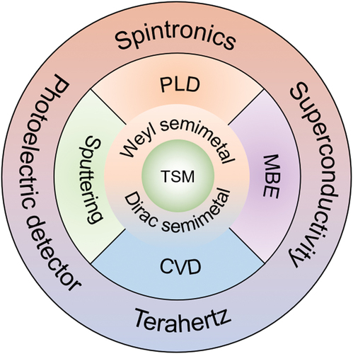
Graphical Abstract
1. Introduction
Materials are traditionally classified into three categories of conductor, semiconductor and insulator according to their electronic properties [Citation1]. Topological materials, as a new category of condensed matter, have evidenced new discovered quantized electrical transport phenomena such as quantum Hall effect (QHE) [Citation2] and quantum anomalous Hall effect (QAHE) [Citation3,Citation4]. The topological nontrivial band structures of topological insulators (TIs) or topological semimetals (TSMs) endow them with novel surface states beyond the bulk ones. In TIs, the conduction and valence bands are inverted by strong spin-orbit coupling (SOC) [Citation5], forming gapless surface states with spin-momentum locking [Citation6]. Such surface states were firstly predicted and demonstrated to exist in HgTe/CdTe quantum wells [Citation7,Citation8] and later found in other TIs like Bi2Se3 [Citation9], Bi2Te3 [Citation10] and Sb2Te3 [Citation11]. The band structure of TIs is topologically protected and can be described by topological invariant Z2 [Citation12].
Studies [Citation13–18] of Dirac semimetals (DSMs) and Weyl semimetals (WSMs) boosted significantly after the exciting discoveries in TIs. In a DSM, two doubly degenerate bands cross in the Brillouin zone, forming a fourfold degenerate Dirac point at the cross point with linear dispersion in all three directions of the momentum space, as shown in ). Dirac fermions, acting as the low-energy excitation of DSM, can be described by the Dirac equation, as seen in Na3Bi [Citation19] and Cd3As2 [Citation20,Citation21]. Either broken time-reversal symmetry or spatial inversion symmetry can change a Dirac point into two Weyl points. Such Weyl points always come in pairs with opposite chirality and can be alternatively defined as monopoles and antimonopoles of Berry curvature [Citation22]. Bands related to topological surface states in WSMs display Fermi arc between two Weyl points, as shown in ). DSMs/WSMs can be divided into two types according to the shape of the Dirac/Weyl cone, which is constrained by the lattice symmetry [Citation23]. For instance, Weyl cones in type-I WSMs are untilted or weakly tilted, accompanied with a point-like Fermi surface when the energy is placed at the type-I Weyl point. In contrast, type-II WSMs host strongly tilted Weyl cones with a Fermi surface consisting of electron and hole pockets that touch at the type-II Weyl points [Citation24], as shown in ). In addition to DSMs and WSMs, nodal-line semimetals have been proved to possess 1D Dirac line or loops close to Fermi level in the momentum space, such as ZrSiX (X = S, Se, and Te) family [Citation25–27]. Recently, two dimensional (2D) layered TSMs have gained intense attention due to their exotic electronic properties and controllable crystalline structures [Citation28,Citation29]. In layered structures, metal layers are sandwiched by adjacent chalcogenide layers and these sandwich structures stack along the c axis and interact with van der Waals forces, as shown in ). According to different stacking modes, layered structures can be divided into hexagonal (2H), trigonal (1T), orthogonal (Td) and distorted trigonal (1T′) structures. The rich crystal structures for different TSMs, such as Td WTe2 [Citation30,Citation31], Td and 1T’ MoTe2 [Citation32,Citation33], 1T PtTe2 [Citation34] and 1T PdTe2 [Citation35], have provided an excellent platform for studying superconductivity [Citation36,Citation37], spintronics [Citation38–42] and valley-optoelectronics [Citation43].
Figure 1. Schematic illustration of the band structures and crystal structures of topological Dirac semimetals and topological Weyl semimetals. (a). The splitting of a Dirac point (DP) into a pair of Weyl points with opposite chirality (WP±) through time-reversal symmetry (TRS) or inversion symmetry (IS) breaking. The green line represents a surface Fermi arc (SFA) between the Weyl points reproduced from reference. Reproduced from [Citation130]. (b). Type-II Weyl semimetal and type-II Dirac semimetal with tilted Weyl or Dirac cones. Reproduced from [Citation130]. (c). Crystal structures of layered topological materials. Blue and purple spheres represent metal and chalcogenide atoms, respectively.
![Figure 1. Schematic illustration of the band structures and crystal structures of topological Dirac semimetals and topological Weyl semimetals. (a). The splitting of a Dirac point (DP) into a pair of Weyl points with opposite chirality (WP±) through time-reversal symmetry (TRS) or inversion symmetry (IS) breaking. The green line represents a surface Fermi arc (SFA) between the Weyl points reproduced from reference. Reproduced from [Citation130]. (b). Type-II Weyl semimetal and type-II Dirac semimetal with tilted Weyl or Dirac cones. Reproduced from [Citation130]. (c). Crystal structures of layered topological materials. Blue and purple spheres represent metal and chalcogenide atoms, respectively.](/cms/asset/29093723-d7a5-4cc1-9715-0369dc278578/tapx_a_2034529_f0001_oc.jpg)
Previous studies on 2D TSMs mainly based on individual films or heterostructures produced by mechanical exfoliation and stacking, which are limited to the small lateral size with poor yielding and not suitable for practical application. To resolve this problem, a variety of techniques have been developed to realize scalable production of large-area, high-quality 2D layered TSM films with controllable thickness. Chemical vapor deposition (CVD) is a universal method to prepare 2D layered films. Using metal films as precursors, centimeter-scale films of various TSMs can be facilely achieved, including WTe2 [Citation44], MoTe2 [Citation45–48] and PtTe2 [Citation49]. In 2017, Tang et al. [Citation50] verified a quantum Hall state in monolayer 1T’-WTe2 grown by molecular beam epitaxy (MBE). Moreover, other methods, such as pulsed laser deposition (PLD) [Citation51–53], sputtering [Citation54], atomic layer deposition (ALD) [Citation55] and metal-organic CVD [Citation56,Citation57] are also developed to fabricate the high-quality 2DTSM films and related heterostructures.
Note that a couple of recently published reviews have fully described the development of topological semimetals [Citation23,Citation24,Citation58,Citation59]. In this mini-review, we shall provide an overview of recent progress in large-area 2DTSM films. We firstly introduce several techniques to fabricate large-area films. Secondly, we summarize the novel electronic properties and potential applications of 2DTSMs. Finally, we will briefly discuss the existed problems and point out the prospects in the future applications of 2D TSMs.
2. Large-area fabrication methods
Although tremendous efforts have been devoted to preparing large-area 2D material films in the last decade, the scalable production of TSM films has not achieved enough attention until more recently. Thanks to numerous successful precedents, the large-area fabrication of TSM films is developing rapidly. At the same time, some unique problems are encountered. In this section, we will extendedly discuss the chemical and physical methods that have been widely employed, and give a brief introduction to the strategies which are still in their infancy to prepared large-area 2D TSM films.
2.1 Chemical vapor deposition
In traditional CVD method, powder precursors sublimate into gas state and react on the surface of substrates to form films. Although numerous layered material films have been synthesized by this method, it is difficult to grow large-area aligned films. Since most layered TSMs contain Te element, it is a facile method to prepare large-area TSM films by tellurizing a pre-deposited metal or metallic oxide film in a CVD furnace. The pre-deposited films can be prepared by sputter, EBE, ALD or thermal evaporation. 1T’ and 2H MoTe2 films can be selectively synthesized by carefully choosing metal film precursor and controlling the growth condition. Zhou et al. [Citation46,Citation47] reported that 1T’ MoTe2 films tended to be obtained under conditions of insufficient Te and with better uniformity from MoO3 precursors. The transformation process from MoO3 to 1T’/2H MoTe2 was clearly investigated and could be regulated by controlling the carrier gas flow rate and tellurization temperature [Citation48,Citation60,Citation61]. To enhance the reactivity of Te and make tellurization process more easily, H2 gas was introduced to form intermediate hydrogen telluride [Citation62], as shown in ). Meanwhile, thickness of the films after tellurization were determined by controlling the initial thickness of precursor MoOx films [Citation62]. Besides, the Te-rich environment can also be obtained by directly placing NixTey films [Citation63] or directly depositing Te thin films [Citation64] on the surface of transition metal film. Compared with Te powder sublimation, these contact methods result in a more homogeneous tellurization. Similar to MoTe2, CVD growth of large-area WTe2 films has been widely reported [Citation44,Citation65] by using W films and Te powder as precursors.
Figure 2. CVD growth of MoTe2 and PtTe2 by tellurizing corresponding metal films. (a). Top is a two-zone furnace growth schematic. Middle and bottom are TEM cross-section images of a 14-cycle MoOx film and converted MoTe2 film, respectively. Reproduced from [Citation62]. (b). Schematic of the CVD process with a half-open quartz tube. Reproduced from [Citation67]. (c). The photograph of wafer-scale PtTe2 films with different thicknesses of ≈ 5 nm (top) and ≈ 10 nm (bottom). Reproduced from [Citation67]. (d). Photo image of PtTe2 films on different substrates. Reproduced from [Citation68].
![Figure 2. CVD growth of MoTe2 and PtTe2 by tellurizing corresponding metal films. (a). Top is a two-zone furnace growth schematic. Middle and bottom are TEM cross-section images of a 14-cycle MoOx film and converted MoTe2 film, respectively. Reproduced from [Citation62]. (b). Schematic of the CVD process with a half-open quartz tube. Reproduced from [Citation67]. (c). The photograph of wafer-scale PtTe2 films with different thicknesses of ≈ 5 nm (top) and ≈ 10 nm (bottom). Reproduced from [Citation67]. (d). Photo image of PtTe2 films on different substrates. Reproduced from [Citation68].](/cms/asset/49a015ad-16a2-4165-8bee-ed6242dd1093/tapx_a_2034529_f0002_oc.jpg)
PtTe2 and PdTe2 are proved to be Dirac semimetals by ARPES and can be prepared by tellurizing metal films. CVD-grown PtTe2 films tend to be polycrystalline [Citation49]. Further study showed a transition of 2D PtTe2 films orientation with increasing thickness, which could affect the electrical conductivity of the films [Citation66]. Wafer-scale PtTe2 thin films were prepared by annealing pre-deposited Pt films on SiO2 substrates in tellurium vapor as shown in [Citation67]. The half-open quartz tubes were utilized to effectively reduce the particle loss and potentially reduce heat loss. High-quality PtTe2 films with giant spin hall conductivity were obtained by this method. Beside SiO2, PtTe2 films were grown on a wide range of substrates [Citation68], such as Si, Al2O3, glass, etc., including NaCl which can be further dissolved to obtain free-standing films as shown in ). Also, the selective preparation of PtTe and PtTe2 phase can be realized by suitably controlling Te steam and the temperature [Citation68]. Unlike other 2D materials, monolayer PtTe2 and PdTe2 films are hard to achieve through exfoliation due to their strong interlayer interaction, but can be prepared by directly tellurizing Pd(111) and Pt(111) single crystals [Citation69].
2.2 Molecular beam epitaxy
MBE is a versatile growth technique to prepare large-area and high-quality crystalline 2D films. Compared with CVD, it offers high flexibility in chemical components, precise control of the film thickness and the ability to grow heterostructures and superlattices with abrupt interfaces. Ultrahigh vacuum (background vacuum up to 10−10 mbar) in the growth chamber during the growth process ensures the purity of the film. Besides, multiple characterization techniques can be integrated with MBE to in situ monitor the growth process and investigate electronic structures, such as reflection high-energy electron diffraction (RHEED) and angle-resolved photoemission spectroscopy (ARPES). Because of these advantages, MBE can be employed in the growth of almost all TSMs like PtTe2 [Citation70–72], PtSe2 [Citation73], PdTe2 [Citation74] and ZrTe2 [Citation75], etc.
Among WSMs, MoTe2 is an interesting material with its hexagonal (2H) phase as a semiconductor and monoclinic (1T’) phase as a type-II WSM. The small energy difference (35 meV per unit) between these two phases makes the selective synthesis of pure-phase films very laborious. 2H-MoTe2 is slightly more stable under ambient conditions and easier to achieve compared with 1T’-MoTe2. ) is a schematic illustration of MBE growth of MoTe2. High-purity Mo and Te molecular beams are evaporated by an e-beam evaporator and a Knudsen cell, respectively [Citation76].
Figure 3. MBE growth of MoTe2 and WTe2 films. (a). Schematic diagram of the MBE growth setup for MoTe2. Reproduced from [Citation76]. (b). Growth process control of the MBE growth of 1T’ and 2H MoTe2. Reproduced from [Citation76]. (c). Raman spectra of the MoTe2 films grown at different temperatures. Reproduced from [Citation76]. (d). RHEED patterns of graphene substrate (top) and sub-monolayer 1T’ WTe2 (bottom). Reproduced from [Citation50]. (e). Core level spectra of 1T’ WTe2. Reproduced from [Citation50]. (f). Atomically resolved STM image of 1T’ WTe2. Reproduced from [Citation50].
![Figure 3. MBE growth of MoTe2 and WTe2 films. (a). Schematic diagram of the MBE growth setup for MoTe2. Reproduced from [Citation76]. (b). Growth process control of the MBE growth of 1T’ and 2H MoTe2. Reproduced from [Citation76]. (c). Raman spectra of the MoTe2 films grown at different temperatures. Reproduced from [Citation76]. (d). RHEED patterns of graphene substrate (top) and sub-monolayer 1T’ WTe2 (bottom). Reproduced from [Citation50]. (e). Core level spectra of 1T’ WTe2. Reproduced from [Citation50]. (f). Atomically resolved STM image of 1T’ WTe2. Reproduced from [Citation50].](/cms/asset/971a0d37-daa8-4ea2-a8da-e9d75b87656d/tapx_a_2034529_f0003_oc.jpg)
MBE growth of 2H MoTe2 was reported on a variety of substrates, such as c-Al2O3(0001) [Citation77], MoS2 [Citation78], CaF2 [Citation79] and GaAs [Citation79]. The similarity of 2H and 1T’ MoTe2 often results in a mixture of these two phases. Monolayer films of mixed 2H and 1T’ MoTe2 were grown on highly oriented pyrolytic graphite (HOPG) substrates [Citation80]. The ratio of 2H to 1T’ phase can be tuned by changing the growth temperature and Te fluxes. Besides, lateral heterophase homojunctions of 2H and 1T’ MoTe2 were observed in MBE grown films, which may have potential in lateral homojunction electronic devices [Citation81]. Later, Tang et al. [Citation82] reported a successful growth of high quality monolayer 1T’ MoTe2 on bilayer graphene terminated 6H-SiC(0001) and confirmed its semimetal properties by ARPES. The 1T’ MoTe2 will normally transfer to the Td phase at a low temperature below 250 K. However, Td MoTe2 can be stabilized at room temperature by growing on InAs(111)/Si(111) substrates [Citation83]. Theoretical and experimental results show that the strain caused by the substrate plays an important role in phase stabilization and band structure engineering [Citation84]. Another key factor in stabilizing the structural phase is the growth temperature [Citation85]. According to He et al. [Citation76], the 2H MoTe2 was observed at a growth temperature between 345–365°C, whereas the 1T’ MoTe2 appeared at a higher temperature between 380–450°C, as shown in –(c).
WTe2 is another type-II WSM and has attracted much attention on its MBE growth. High quality 1T’ WTe2 films have been successfully grown on 2D (Bi2Te3, MoS2, and graphite) [Citation86] and 3D (c-Al2O3) [Citation87] material substrates. Besides, monolayer 1T’ WTe2 was predicted and confirmed to be a quantum spin Hall insulator with topological protected edge states and its epitaxial growth has also been widely reported [Citation88–90]. ) shows the RHEED patterns of the graphene substrate and monolayer WTe2 grown by MBE [Citation50], demonstrating the layer-by-layer growth mode. A pure 1T’ WTe2 phase with a small angle distortion is verified by further angle-integrated core level photoemission combined with scanning tunneling microscopy characterization [Citation50], as shown in –(f).
2.3 Pulsed laser deposition
The PLD technique utilizes a focused high-energy pulsed laser to bombard the target and convert the solid material of a small area into the plasma state, as called the plume. The focused laser pulse can raise the temperature of the micro-region up to ten thousand degrees in a very short time. As such, the PLD technique is very suitable for depositing high-melting-point materials and has no composition selectivity. PLD has many advantages for depositing 2D materials, such as high growth rate, clean fabrication process and relatively low growth temperature [Citation91]. Meanwhile, it allows homogeneous growth of high-quality centimeter-scale films. Besides, the thickness of the films can be readily controlled by changing the number of laser pulses, making PLD very suitable for industrial production.
PLD has promoted the development of photodetectors based on 2D materials like 2H-MoTe2 [Citation51]. In the last few years, several 2D TSM films [Citation92,Citation93] have been produced by PLD. ) shows a two-step synthesis to prepare WTe2 thin films [Citation94]. The amorphous WTe2 films were firstly deposited on cleaned mica by PLD method, and then sealed in a quartz tube with the added Te powder and annealed at 700°C for days to crystallize. The raman spectrum in ) shows good crystallinity of the films. Distinct Shubnikov-de Haas Oscillations [Citation94] and tunable magnetoresistance [Citation52] were observed in these large-area films, even after transferring to other substrates [Citation95]. However, this two-step method is time-consuming and easy to introduce impurities during the annealing process. Very recently, a single-step method was reported. single-crystal-like 1T’ WTe2 films were successfully grown on Bi2Te3 seeded layer by using single-crystal target at a low temperature (210°C) [Citation96]. Clear crystalline structures and abrupt interfaces of multilayered Bi2Te3-WTe2 heterostructures can be seen in the scanning transmission electron microscopic image in high-angle annular dark field (HAADF) mode, as shown in –(d). In addition, topological material candidate ZrTe2 films were grown on (110)-oriented SrTiO3(STO) substrates and protected by in-situ deposition of a AlN capping layer [Citation97]. A large magnetoresistance (∼3000% at 2 K and 9 T) was observed in these films, which could benefit their application in magnetoresistance type sensors.
Figure 4. Preparation and characterization of PLD growth of WTe2 films. (a). Schematic diagrams of the PLD and post annealing apparatus for WTe2 films. Reproduced from [Citation94]. (b). Raman spectra of the WTe2 films annealed for different time intervals. Reproduced from [Citation94]. (c). Cross-section HAADF image of a multilayered Bi2Te3-WTe2 film grown on mica. Reproduced from [Citation96]. (d). Higher magnification scan of the boxed area shown in Figure 4(c). Reproduced from [Citation96].
![Figure 4. Preparation and characterization of PLD growth of WTe2 films. (a). Schematic diagrams of the PLD and post annealing apparatus for WTe2 films. Reproduced from [Citation94]. (b). Raman spectra of the WTe2 films annealed for different time intervals. Reproduced from [Citation94]. (c). Cross-section HAADF image of a multilayered Bi2Te3-WTe2 film grown on mica. Reproduced from [Citation96]. (d). Higher magnification scan of the boxed area shown in Figure 4(c). Reproduced from [Citation96].](/cms/asset/736ff4f0-44e1-4afe-8f8a-aab7bc883563/tapx_a_2034529_f0004_oc.jpg)
In conclusion, TSM films grown by PLD have developed rapidly in recent years. They exhibit high-quality structures and exotic electronic properties for electronic and optoelectronic devices. Meanwhile, there is still plenty room for developing PLD technique for other TSM films beyond the discovered ones. We believe that with increasing attention, this technique will significantly promote the commercial application of TSMs in the future.
2.4 Sputtering
Sputtering is a widely used technique for the deposition of both metal and alloy thin films and has been utilized in numerous industrial productions. During sputtering deposition, glow discharge is first created in inert gas to produce energetic electrons and ions. The electrons will collide with gas atoms and create secondary electrons and more ions to maintain the discharge. Then the created ions of the inert gas are accelerated toward and subsequently bombard the target. As a result, the sputtered species will leave the target and carry enough kinetic energy to reach the substrate and form films. Sputtering deposition is an ideal technique for the fabrication of TSM films due to its high deposition rate and wafer-scale production. Sputtered WTe2 and MoTe2 films have been used to study pulsed laser generation [Citation98,Citation99] and spin-to-charge conversion [Citation100,Citation101].
In 2017, Huang et al. [Citation102] reported a successful growth of MoTe2 films by sputtering. As shown in ), with the protection of the SiO2 layer, the as-deposited MoTe2 films with low crystallinity initially form 1T’ structure and convert gradually to 2H structure over a prolonged annealing time at 650°C. The transition process of as-deposited films was also clearly verified in another report [Citation103] as shown in ). Also, co-sputtering technique [Citation54,Citation104] was used to grow 1T’-MoTe2 films under low temperature. As shown in ), Mo and Te atoms were co-deposited onto graphene surfaces at room temperature. The sticking coefficients of Mo and Te were investigated by changing the substrate temperature ()). Further ex situ thermal annealing in the Te environment could increase the stoichiometry of MoTe2 films [Citation54]. As evidenced by numerous reports, the post-annealing plays an important role in improving the crystallization and stoichiometry of sputtered TSM films.
Figure 5. (a). Schematic illustration of the post annealing SiO2/MoTe2/SiO2 heterostructure. Reproduced from [Citation102]. (b). Schematic diagram of the co-sputtering deposition of MoTe2. Reproduced from [Citation54]. (c). Plot of deposition rate and the Te/Mo ratio (inset) vs. temperature. Reproduced from [Citation54]. (d). Schematic illustration of the transformation of the as-deposited MoTe2 films. Reproduced from [Citation103].
![Figure 5. (a). Schematic illustration of the post annealing SiO2/MoTe2/SiO2 heterostructure. Reproduced from [Citation102]. (b). Schematic diagram of the co-sputtering deposition of MoTe2. Reproduced from [Citation54]. (c). Plot of deposition rate and the Te/Mo ratio (inset) vs. temperature. Reproduced from [Citation54]. (d). Schematic illustration of the transformation of the as-deposited MoTe2 films. Reproduced from [Citation103].](/cms/asset/ece9e60b-b969-4e47-8245-f6d444a11230/tapx_a_2034529_f0005_oc.jpg)
2.5 Comparison of different fabrication methods
is a list of representative reports of fabricating large-area 2D layered topological semimetal films. The growth temperatures are significantly different in different preparation methods. The growth temperature of the CVD method is relatively high, ranging from 500–800°C, while that of MBE, PLD and sputtering is relatively low, about 300°C. In the choice of the substrate, the CVD method has no special requirements for the substrate, so silicon-based substrates are usually used for industrial compatibility. The MBE method usually uses a substrate with a matching lattice structure to achieve epitaxial growth, such as SiC (0001) and a two-dimensional material substrate. The as-deposited films grown by PLD and sputtering tend to be amorphous, but after annealing at high temperature, the crystalline properties can be significantly improved.
Table 1. List of large-area growth conditions for 2D layered topological semimetals
3. Applications
TSMs have exhibited great potential in new generation electronic devices due to their novel surface states and exotic transport properties. Developments of large-area production further foster their practical application. In this section, we mainly review research on applications of large-area TSM films in field of superconductivity, optical response and spintronics.
3.1 Superconductivity
Plenty of 2D layered TSMs are proven to be superconductive under certain conditions, like WTe2 [Citation37], MoTe2 [Citation36] and Ir1-xPtxTe2 [Citation105]. Interestingly, an unconventional magnetic field enhanced superconductivity was discovered in MBE grown WTe2 [Citation87], which might result from the lifting of inversion symmetry. As for the Pt-based TSMs, PtTe2 has a low Tc of below 0.002 K due to the weak of electron–phonon coupling, which is difficult for applications even in basic sciences [Citation106,Citation107]. There are many methods for improving the Tc, e.g. electron doping [Citation108] or alkali-metal intercalations [Citation109]. Although PdTe2 and PtTe2 have similar crystal structures and band structures, PdTe2 has a higher Tc (~ 1.7 K) due to its strong electron-phonon coupling strength [Citation109,Citation110]. Meanwhile, the topological state of the Dirac cone has little influence on the superconductivity state, which is more favorable for the study of the superconductivity characteristics of PdTe2 [Citation111].
After the finding of type-II Dirac fermions in PtSe2-type transition metal dichalcogenides, bulk PdTe2 was proven to possess both superconductivity and tilted Dirac cone. Liu et al. [Citation112] prepared PdTe2 films with various thicknesses from 2-ML to 20-ML on STO substrates by MBE and investigated the electronic and superconducting properties ()). The monolayer PdTe2 films showed narrow-band gap semiconductor behavior, while multilayer films exhibited good superconductivity. The Tc of the ultra-thin film was significantly higher than that of the classical theoretical formula and could be further increased by Mg intercalation [Citation112], as shown in ). Y. Liu et al. [Citation113] observed abnormal metal states at low temperature in ultra-thin single crystal PdTe2 films compared with traditional superconductor. Their resistance tended to reach a saturation value at extremely low temperature under the condition of high-quality filter measurement ()). Meanwhile, the superconducting characteristics of the film remained almost unchanged within 20 months. At the same time, they also observed Quantum Griffiths Singularity (QGS) in a 4-ML PdTe2 film under both perpendicular and the parallel magnetic fields [Citation74], as shown in ). However, with the increase of film thickness to 6-ML, the QGS gradually disappeared under a parallel field but still maintained under a perpendicular field, which can promote the further study of novel quantum phase transitions induced by a parallel magnetic field.
Figure 6. The transport characteristics of the MBE growth PdTe2 films. (a). The resistance of PdTe2 films with different thickness as a function of the temperature. The inset is the schematic of four-probe measurements. Reproduced from [Citation112]. (b). Tc and Hc2 (T = 0) dependence of the film thickness. The circles and squares represent the Hc2 (0) derived from the two-band model and Ginzburg-Landau formula, respectively. Reproduced from [Citation112]. (c). The sheet resistance Rs of PdTe2 films under the conditions of different perpendicular magnetic fields from 0 to 0.897 T. Reproduced from [Citation113]. (d). The evolution of Rs-B curves at different temperatures ranging from 20 to 450 mK. The inset curves are some crossing points from the Rs-B. Reproduced from [Citation74].
![Figure 6. The transport characteristics of the MBE growth PdTe2 films. (a). The resistance of PdTe2 films with different thickness as a function of the temperature. The inset is the schematic of four-probe measurements. Reproduced from [Citation112]. (b). Tc and Hc2 (T = 0) dependence of the film thickness. The circles and squares represent the Hc2 (0) derived from the two-band model and Ginzburg-Landau formula, respectively. Reproduced from [Citation112]. (c). The sheet resistance Rs of PdTe2 films under the conditions of different perpendicular magnetic fields from 0 to 0.897 T. Reproduced from [Citation113]. (d). The evolution of Rs-B curves at different temperatures ranging from 20 to 450 mK. The inset curves are some crossing points from the Rs-B. Reproduced from [Citation74].](/cms/asset/558c0676-74fc-469d-b860-d3dc27de549a/tapx_a_2034529_f0006_oc.jpg)
3.2 Optoelectronics
As a type II Dirac semimetal, PtTe2 shows a strongly tilted Dirac cone along some momentum directions, which violates Lorentz invariance and protects the gapless band structure by crystal symmetry [Citation114]. The characteristics of high carrier mobility, ultrafast photo response and low photocurrent make PtTe2 an ideal material for near/mid-infrared (NIR/MIR) and terahertz (THz) detection [Citation115–117]. Wei et al. [Citation72] prepared high-quality PtTe2 films by MBE, which showed high sensitivity at 960 nm wavelength ()), up to 15.6 mA·W−1. Meanwhile, the films have an anisotropic optical response with wavelength dependency. When the scanning wavelength is 10.7 μm, the ratio of anisotropy ellipse reaches 8.3, indicating that the optical response of PtTe2 exhibits stronger anisotropy under low energy excitation [Citation72], as shown in ). This is very important for the study of polarization angle-sensitive detection. To quantify the response speed precisely, a 625 nm wavelength light is used to irradiate the PtTe2/p-Si device as demonstrated in ) [Citation49]. According to the photocurrent at different optical frequencies, the relative balance changes ~ 5% in the frequency range of 100 kHz and remains ~80.6% even at a very high frequency of 300 kHz ()). In addition, the rise and fall times of ~1.68 μs and ~ 1.58 μs at an optical frequency of 150 kHz are measured, respectively ()), which are lower than those of most 2D/2D or 2D/3D materials. Tong et al [Citation118] used lithography to assemble 64-pixel PtTe2-based NIRPD arrays on SiO2/Si chips, showing good resolution in near-infrared imaging, as shown in ). The five letters ‘N I R P D’ can be clearly seen due to the sharp contrast with the background, indicating that the PtTe2-based arrays have great potential in the next generation of optoelectronics technology. Besides, PtTe2 also shows a high-performing photodetection system in the THz band [Citation119,Citation120]. Xu et al. [Citation121] fabricated the THz detection devices based on PtTe2 with bow-tie-type planar contacts ( –(h)), which showed a high photoresponsivity (1.6 A W−1 without bias voltage) with a response time less than 20 µs, while the detectors based on vertically stacked PtTe2 and graphene heterostructures reached responsivity above 1.4 kV W−1 and a response time shorter than 9 µs. Additionally, an impressive THz image of the metal nut inside the envelope is shown in ). Other topologically related optical responses, such as plasmons [Citation44] and nonlinear absorption [Citation92,Citation93] have been observed in large-area WTe2 films and require further realization in other 2D layered TSM films.
Figure 7. Photoelectric detection researches of PtTe2 films. (a). The photoresponse of PtTe2 at different wavelengths. The inset is the schematic illustration of photodetector. Reproduced from [Citation72]. (b). Anisotropic photoresponse for the linear-polarized excitation at 10.7 μm. Reproduced from [Citation72]. (c). The schematic illustration of the temporal photo-responsiveness of PtTe2/p-Si devices. Reproduced from [Citation49]. (d). Relative balance as a function of illumination modulation frequency, defined as (Imax− Imin)/Imax. Reproduced from [Citation49]. (e). The rise (τr) and fall (τf) times are obtained in the magnified view of photo-switching characteristics at 150 kHz. Reproduced from [Citation49]. (f). Photographs and images of the PtTe2-based arrays device. Reproduced from [Citation118]. (g), (h). The THz detecting devices and mechanisms of PtTe2 and graphene heterojunction, respectively. Reproduced from [Citation121]. (i). THz image of the metal nut. Reproduced from [Citation121].
![Figure 7. Photoelectric detection researches of PtTe2 films. (a). The photoresponse of PtTe2 at different wavelengths. The inset is the schematic illustration of photodetector. Reproduced from [Citation72]. (b). Anisotropic photoresponse for the linear-polarized excitation at 10.7 μm. Reproduced from [Citation72]. (c). The schematic illustration of the temporal photo-responsiveness of PtTe2/p-Si devices. Reproduced from [Citation49]. (d). Relative balance as a function of illumination modulation frequency, defined as (Imax− Imin)/Imax. Reproduced from [Citation49]. (e). The rise (τr) and fall (τf) times are obtained in the magnified view of photo-switching characteristics at 150 kHz. Reproduced from [Citation49]. (f). Photographs and images of the PtTe2-based arrays device. Reproduced from [Citation118]. (g), (h). The THz detecting devices and mechanisms of PtTe2 and graphene heterojunction, respectively. Reproduced from [Citation121]. (i). THz image of the metal nut. Reproduced from [Citation121].](/cms/asset/e71f9b1b-810f-41e2-9303-797a3f673b10/tapx_a_2034529_f0007_oc.jpg)
3.3 Spintronics
With the rapid development of spintronics, magnetic random access memory (MRAM) devices based on spin transfer toque (STT) or spin orbit toque (SOT) have attracted considerable attention due to their fast response, non-volatile memory and low power consumption. Further development of STT/SOT-MRAM devices demands highly efficient spin-to-charge conversion materials. In previous studies, heavy metals were widely used as spin sources. Recently, the discovery of topological quantum materials has opened a new area for the design of spintronic devices. In TSMs, the topological surface states are spin-momentum locking, resulting in highly efficient spin-to-charge conversion. Besides, low symmetric crystal structures of layered TSMs lead to out-of-plane spin polarized current, which can directly switch perpendicular magnetization material without an external field. Studies of spin orbit toque have been reported in WTe2 [Citation38,Citation40,Citation122–124] and MoTe2 [Citation41,Citation42] based on exfoliation flakes. To meet the demand for industrial fabrication, research on large-area TSM films has been carried out.
Fan et al. [Citation100] studied the spin-charge conversion of amorphous WTe2 grown on Co20Fe60B20 by sputtering. Spin pumping and second harmonic Hall measurements showed a large field-like (FL) toque contrast to a small damping-like (DL) toque attributed to the spin swapping effect ( –(b)). However, a large DL toque is found in the sputtered WTe2/CoTb heterostructure. This indicates that the composition of WTe2 may strongly affect the spin-charge conversion [Citation101], as shown in ) and 8(c). In addition, Shi et al [Citation125] estimated in-plane and out-of-plane spin conductivities close to 7.36 × 10³ (ℏ/2e) (Ωm)–1 and 1.76 × 10³ (ℏ/2e) (Ωm)–1 in a centimeter-scale CVD growth Td-WTe2. ) and 8e are schematic illustrations and images of the Py/WTe2 devices. Magnetization switching was further demonstrated by the magneto-optical Kerr effect (MOKE) [Citation125], as shown in ). The switching current density is as low as 105 A cm−2, which is 1–2 orders of magnitude smaller than the typical value of 106–107 A cm−2 in HMs [Citation126]. Compared with other transition metal dichalcogenides (TMDs), PtTe2 exhibits the large spin Hall conductivity because of its high conductivity and strong spin-orbit coupling. Through spin-torque ferromagnetic resonance measurements ()), PtTe2 presents a larger SOT efficiency (ξSOT ≈ 0.152) than Pt (ξSOT ≈ 0.058) [Citation67], as shown in –(i), which exhibits great potential in wafer-scale spintronic device applications.
Figure 8. The spin orbit torque measurements in the WSMs and DSMs. (a). Illustration of the second harmonic measurement on WTex(3, 5, 8 nm)/CoFeB(6 nm) Hall bar device. Reproduced from [Citation100]. (b). The thickness dependent DL torque and FL torque of the sample in Figure 8(a). Reproduced from [Citation100]. (c). The DL torque efficiency of different thickness and Te concentration in WTex films. Reproduced from [Citation101]. (d), (e). The schematic illustration and image of the Py/WTe2 devices. Reproduced from [Citation125]. (f). MOKE images of Py before (left) and after (right) applying a pulsed DC current I (indicated by the purple arrow) along the x-axis. Reproduced from [Citation125]. (g). The schematic illustration of the torque generation in the Py/PtTe2 heterojunction. Reproduced from [Citation67]. (h). The inverse of the SOT efficiency as an evolution of the inverse of the Py thickness in Pt/Py and PtTe2/Py. Reproduced from [Citation67]. (i). ξSOT (circle line) and spin Hall conductivity (circle) with different PtTe2 thicknesses. Reproduced from [Citation67].
![Figure 8. The spin orbit torque measurements in the WSMs and DSMs. (a). Illustration of the second harmonic measurement on WTex(3, 5, 8 nm)/CoFeB(6 nm) Hall bar device. Reproduced from [Citation100]. (b). The thickness dependent DL torque and FL torque of the sample in Figure 8(a). Reproduced from [Citation100]. (c). The DL torque efficiency of different thickness and Te concentration in WTex films. Reproduced from [Citation101]. (d), (e). The schematic illustration and image of the Py/WTe2 devices. Reproduced from [Citation125]. (f). MOKE images of Py before (left) and after (right) applying a pulsed DC current I (indicated by the purple arrow) along the x-axis. Reproduced from [Citation125]. (g). The schematic illustration of the torque generation in the Py/PtTe2 heterojunction. Reproduced from [Citation67]. (h). The inverse of the SOT efficiency as an evolution of the inverse of the Py thickness in Pt/Py and PtTe2/Py. Reproduced from [Citation67]. (i). ξSOT (circle line) and spin Hall conductivity (circle) with different PtTe2 thicknesses. Reproduced from [Citation67].](/cms/asset/da4c503f-5ac6-4312-b7e2-412efe6a90c7/tapx_a_2034529_f0008_oc.jpg)
Conclusion and outlook
Recent studies on layered topological semimetals have proven their potential for many applications like superconductive devices, optical devices and spintronic devices. Efforts on the large-area fabrication of 2D layered TSM films further enhance the possibility for practical applications. There is no doubt that TSMs will continuously attract attention and effort from researchers. Here we suggest several topics to be concerned. We expect that 2D layered TSMs can quickly enter commercial applications after addressing the following issues.
(1) Compared with 2D semiconductors which have been intensively studied, experience in preparing TSMs in large area is still lacking. Although various fabrication techniques have been reported, a universal method to produce high-quality and wafer-scale films with low cost and high yield has yet to be developed. Growing epitaxial thin films of certain materials such as MoTe2 and WTe2 is still challenging because of the weak bonding energy and large vapour pressure difference between metal and Te atoms. Mo(W) atoms tend to bond with each other rather than form layered structure with Te, leading to the Te-deficiency formation. Moreover, Mo(W)Te2 will decompose and lose Te as vapour at high temperature [Citation46]. Due to these properties, it is difficult to directly obtain high-quality films by PVD methods, especially methods that rely on vaporizing compound targets. Post annealing in Te atmosphere may both improve the crystallinity and complement Te of as-deposited films [Citation52]. In MBE growth, the flux ratio of Te/Mo(W) is usually kept at tens or even hundreds [Citation77,Citation80,Citation86] to ensure the stoichiometric ratio of films.
(2) Another issue caused by weak bonding energy between Mo(W) and Te is the chemical instability of thin films. Exposure to air may induce surface oxidation of the films, resulting in degradation of electrical properties. For example, amorphous MoO3–TeO2 surface layers were observed in oxidized 1T′-MoTe2 films and significantly enlarged the resistance [Citation127]. In addition, the magnetoresistance of WTe2 thin films increased about 30% after exposure to air for 30 days, which resulted from the p-type doping by surface WOx layer [Citation128]. Since oxidation layers can remarkably change the intrinsic properties of bottom films, how to keep the prepared film stable in the ambient is the critical issue for practical applications. One feasible approach is to in situ depositing capping layers like AlN [Citation97] and SiO2 [Citation102] that can protect TSM films from moisture and air. Meanwhile, we should explore more novel materials that are chemically stable in the air, like PdTe2, PtTe2, and PtSe2.
(3) Since the critical superconducting temperature of TSMs is generally below 2 K, it seems to be an arduous task for basic research. Improving the Tc of the TSMs appears to be of great importance, which is conducive to understanding the relationship between the topology and the superconductivity of the TSMs. The core of increasing Tc is to increase the carrier concentration near the Fermi surface. For Pt-based TSMs, electron doping is one of the most effective means to enhance Tc, which can increase the Tc of PtSe2 and PtTe2 up to 2.15 K [Citation109] and 8 K [Citation108], respectively.
(4) Heterostructures consisting of TSMs and other materials could provide a new platform for theoretical research and practical applications. A TSM/semiconductor heterostructure can be used as an electrical contact for FETs based on TMDs. In analogy with TI/ferromagnetic material (FM) structures [Citation129], TSM/FM structures may trigger the new development in studying proximity coupling and spintronics devices. Besides, photoemission and photodetector in the near-infrared to THz range could be promising areas for TSMs. Furthermore, during the preparation of the ferromagnetic heavy metal and TSM heterostructures, the bottom layered materials will inevitably be damaged by the high-energy ion, leading to more spin loss at the interface during the process of spin-charge conversion. Thus, design of the all van-der Waals epitaxial heterojunction is obviously essential.
Acknowledgments
We thank R. Liu and C. Zhang for the helpful suggestions.
Disclosure statement
No potential conflict of interest was reported by the author(s).
Additional information
Funding
References
- Wang S, Lin B-C, Wang A-Q, et al. Quantum transport in dirac and Weyl semimetals: a review. ADV PHYS-X. 2017;2:518–24.
- Klitzing K, Dorda G, Pepper M. New method for high-accuracy determination of the fine-structure constant based on quantized hall resistance. Phys Rev Lett. 1980;45:494–497.
- Fei F-C, Zhang S, Zhang M-H, et al. The material efforts for quantized hall devices based on topological insulators. Adv Mater. 2020;32:1904593.
- Haldane FD. Model for a quantum hall effect without landau levels: condensed-matter realization of the “parity anomaly”. Phys Rev Lett. 1988;61:2015–2018.
- Yan B-H, Felser C. Topological materials: WEYL semimetals. Annu Rev Condens Matter Phys. 2017;8:337–354.
- Zhang M-H, Wang X-F, Song F-Q, et al. Electrical spin polarization through spin–momentum locking in topological-insulator nanostructures. Chin Phys B. 2018;27:097307.
- Bernevig BA, Hughes TL, Zhang S-C. Quantum spin Hall effect and topological phase transition in HgTe quantum wells. Science. 2016;314:1757–1761.
- König M, Wiedmann S, Brüne C. Quantum spin Hall insulator state in HgTe quantum wells. Science. 2007;318:766–770.
- Hsieh D, Xia Y, Qian D, et al. A tunable topological insulator in the spin helical dirac transport regime. Nature. 2009;460:1101–1105.
- Chen YL, Analytis JG, Chu JH, et al. experimental realization of a three-dimensional topological insulator, bi2te3. Science. 2009;325:178–181.
- Zhang H, Liu C-X, Qi X-L, et al. Topological insulators in Bi2Se3, Bi2Te3 and Sb2Te3 with a single Dirac cone on the surface. Nat Phys. 2009;5:438–442.
- Hasan MZ, Kane CL. Colloquium: topological insulators. Rev Mod Phys. 2010;82:3045–3067.
- Xu S-Y, Belopolski I, Alidoust N. Discovery of a weyl fermion semimetal and topological fermi arcs. Science. 2015;349:613–617.
- Liu Z-K, Zhou B, Zhang Y. Discovery of a three-dimensional topological dirac semimetal, Na3Bi. Science. 2014;343:864–867.
- Burkov AA, Balents L. Weyl semimetal in a topological insulator multilayer. Phys Rev Lett. 2011;107:127205.
- Wan X, Turner AM, Vishwanath A, et al. Topological semimetal and fermi-arc surface states in the electronic structure of pyrochlore iridates. Phys Rev B. 2011;83:205101.
- Lv B-Q, Weng H-M, Fu -B-B, et al. Experimental discovery of Weyl semimetal TaAs. Phys Rev X. 2015;5:031013.
- Armitage NP, Mele EJ, Vishwanath A. Weyl and Dirac semimetals in three-dimensional solids. Rev Mod Phys. 2018;90:015001.
- Di Bernardo I, Hellerstedt J, Liu C, et al. Progress in epitaxial thin-film Na3Bi as a topological electronic material. Adv Mater. 2021;33:2005897.
- Wang Z-J, Weng H-M, Wu Q-S, et al. Three-dimensional Dirac semimetal and quantum transport in Cd3As2. Phys Rev B. 2013;88:125427.
- Zhang K, Pan H-Y, Zhang M-H, et al. Controllable synthesis and magnetotransport properties of Cd3As2 Dirac semimetal nanostructures. RSC Adv. 2017;7:17689–17696.
- Narang P, Garcia CAC, Felser C. The topology of electronic band structures. Nat Mater. 2021;20:293–300.
- Lv B-Q, Qian T, Ding H. Experimental perspective on three-dimensional topological semimetals. Rev Mod Phys. 2021;93:025002.
- Hu J, Xu S-Y, Ni N, et al. Transport of topological semimetals. Annu Rev Mater Sci. 2019;49:207–252.
- Pan H, Tong B, Yu J, et al. Three-dimensional anisotropic magnetoresistance in the Dirac node-line material ZrSiSe. Sci Rep. 2018;8:9340.
- Hu J, Tang Z, Liu J, et al. Evidence of topological nodal-line fermions in ZrSiSe and ZrSiTe. Phys Rev Lett. 2016;117:016602.
- Schoop LM, Ali MN, Strasser C, et al. Dirac cone protected by non-symmorphic symmetry and three-dimensional Dirac line node in ZrSiS. Nat Commun. 2016;7:11696.
- Ali MN, Xiong J, Flynn S, et al. Large, non-saturating magnetoresistance in WTe2. Nature. 2014;514:205–208.
- Duerloo KA, Li Y, Reed EJ. Structural phase transitions in two-dimensional Mo- and W-dichalcogenide monolayers. Nat Commun. 2014;5:4214.
- Pletikosic I, Ali MN, Fedorov AV, et al. Electronic structure basis for the extraordinary magnetoresistance in WTe2. Phys Rev Lett. 2014;113:216601.
- Jiang J, Tang F, Pan X-C, et al. Signature of strong spin-orbital coupling in the large nonsaturating magnetoresistance material WTe2. Phys Rev Lett. 2015;115:166601.
- Sun Y, Wu S-C, Ali MN, et al. Prediction of Weyl semimetal in orthorhombic MoTe2. Phys Rev B. 2015;92:161107.
- Deng K, Wan G-L, Deng P, et al. Experimental observation of topological Fermi arcs in type-II Weyl semimetal MoTe2. Nat Phys. 2016;12:1105–1110.
- Yan M, Huang H, Zhang K, et al. Lorentz-violating type-II Dirac fermions in transition metal dichalcogenide PtTe2. Nat Commun. 2017;8:257.
- Fei F-C, Bo X-Y, Wang R, et al. Nontrivial Berry phase and type-II Dirac transport in the layered material PdTe2. Phys Rev B. 2017;96:041201.
- Qi Y, Naumov PG, Ali MN, et al. Superconductivity in Weyl semimetal candidate MoTe2. Nat Commun. 2016;7:11038.
- Kang D, Zhou Y, Yi W, et al. Superconductivity emerging from a suppressed large magnetoresistant state in tungsten ditelluride. Nat Commun. 2015;6:7804.
- Li P, Wu W, Wen Y, et al. Spin-momentum locking and spin-orbit torques in magnetic nano-heterojunctions composed of Weyl semimetal WTe2. Nat Commun. 2018;9:3990.
- Stiehl GM, Li R, Gupta V, et al. Layer-dependent spin-orbit torques generated by the centrosymmetric transition metal dichalcogenide β−MoTe2. Phys Rev B. 2019;100:184402.
- Zhao B, Karpiak B, Khokhriakov D, et al. Unconventional Charge–Spin Conversion in Weyl-Semimetal WTe2. Adv Mater. 2020;32:2000818.
- Liang S, Shi S, Hsu CH, et al. Spin-orbit torque magnetization switching in MoTe2/permalloy heterostructures. Adv Mater. 2020;32:2002799.
- Safeer CK, Ontoso N, Ingla-Aynes J, et al. Large multidirectional spin-to-charge conversion in low-symmetry semimetal MoTe2 at room temperature. Nano Lett. 2019;19:8758–8766.
- Ye-Quan C, Zhen-Dong C, Yong-Da C. Anisotropic ultrafast spin/valley dynamics in WTe2 films. arXiv:2008.08785.
- Wang C, Sun -Y-Y, Huang S-Y, et al. Tunable plasmons in large-area WTe2 thin films. Phys Rev Appl. 2021;15:014010.
- Park JC, Yun SJ, Kim H. Phase-engineered synthesis of centimeter-scale 1T′- and 2H-molybdenum ditelluride thin films. ACS Nano. 2015;9:6548–6554.
- Zhou L, Xu K, Zubair A, et al. Large-Area Synthesis of High-Quality Uniform Few-Layer MoTe2. J Am Chem Soc. 2015;137:11892–11895.
- Zhou L, Zubair A, Wang Z, et al. Synthesis of high-quality large-area homogenous 1T’ MoTe2 from chemical vapor deposition. Adv Mater. 2016;28:9526–9531.
- Yang L, Zhang W, Li J, et al. Tellurization velocity-dependent metallic-semiconducting-metallic phase evolution in chemical vapor deposition growth of large-area, few-layer MoTe2. ACS Nano. 2017;11:1964–1972.
- Shawkat MS, Chowdhury TA, Chung HS, et al. Large-area 2D PtTe2/silicon vertical-junction devices with ultrafast and high-sensitivity photodetection and photovoltaic enhancement by integrating water droplets. Nanoscale. 2020;12:23116–23124.
- Tang S, Zhang C, Wong D, et al. Quantum spin Hall state in monolayer 1T’-WTe2. Nat Phys. 2017;13:683–687.
- Lu Z, Xu Y, Yu Y, et al. Ultrahigh speed and broadband few‐Layer MoTe2/Si 2D–3D heterojunction‐based photodiodes fabricated by pulsed laser deposition. Adv Funct Mater. 2020;30:1907951.
- Gao M, Zhang M, Niu W, et al. Tuning the transport behavior of centimeter-scale WTe2 ultrathin films fabricated by pulsed laser deposition. Appl Phys Lett. 2017;111:031906.
- Yao JD, Zheng ZQ, Yang GW. Production of large-area 2D materials for high-performance photodetectors by pulsed-laser deposition. Prog Mater Sci. 2019;106:100573.
- Yumigeta K, Kopas C, Blei M, et al. Low-temperature synthesis of 2D anisotropic MoTe2 using a high-pressure soft sputtering technique. Nanoscale Advances. 2020; 2: 1443–1448.
- Mattinen M, Leskelä M, Ritala M. Atomic layer deposition of 2D metal dichalcogenides for electronics, catalysis, energy storage, and beyond. Adv Mater Interfaces. 2021;8:2001677.
- Kim T, Park H, Joung D, et al. Wafer-scale epitaxial 1T′, 1T′-2H mixed, and 2H phases MoTe2 thin films grown by metal-organic chemical vapor deposition. Adv Mater Interfaces. 2018;5:1800439.
- Kim D, Lee R, Kim S, et al. Two-dimensional phase-engineered 1T′– and 2H–MoTe2-based near-infrared photodetectors with ultra-fast response. J Alloys Compd. 2019;789:960–965.
- Ma J, Deng K, Zheng L, et al. Experimental progress on layered topological semimetals. 2D Mater. 2019;6:032001.
- Zhang M, Wang X, Song F, et al. Layered topological insulators and semimetals for magnetoresistance type sensors. Adv Quantum Technol. 2018;2:1800039.
- Sánchez-Montejo E, Santana G, Domínguez A, et al. Phase stability in MoTe2 prepared by low temperature Mo tellurization using close space isothermal Te annealing. Mater Chem Phys. 2017;198:317–323.
- Sun L, Ding M, Li J, et al. Phase-controlled large-area growth of MoTe2 and MoTe2-xOx/MoTe2 heterostructures for tunable memristive behavior. Appl Surf Sci. 2019;496:143687.
- Hynek DJ, Singhania RM, Xu S, et al. cm(2)-scale synthesis of MoTe2 thin films with large grains and layer control. ACS Nano. 2021;15:410–418.
- Song S, Sim Y, Kim S-Y, et al. Wafer-scale production of patterned transition metal ditelluride layers for two-dimensional metal–semiconductor contacts at the Schottky–Mott limit. Nat Electron. 2020;3:207–215.
- Xie S, Chen L, Zhang T-B, et al. Fast solid-phase synthesis of large-area few-layer 1T’-MoTe2 films. J Cryst Growth. 2017;467:29–33.
- Zhou Y, Jang H, Woods JM, et al. Wafer-scale growth of 2D PtTe2 with layer orientation tunable high electrical conductivity and superior hydrophobicity. Adv Funct Mater. 2017;27:1605928.
- Wang M, Ko TJ, Shawkat MS, et al. Wafer-scale growth of 2D PtTe2 with layer orientation tunable high electrical conductivity and superior hydrophobicity. ACS Appl Mater Interfaces. 2020;12:10839–10851.
- Xu H, Wei J, Zhou H, et al. High spin hall conductivity in large‐area type‐II Dirac semimetal PtTe2. Adv Mater. 2020;32:2000513.
- Zhang K, Wang M, Zhou X, et al. Growth of large scale PtTe, PtTe2 and PtSe2 films on a wide range of substrates. Nano Res. 2020;14:1663–1667.
- Liu L, Zemlyanov D, Chen YP. Epitaxial growth of monolayer PdTe2 and patterned PtTe2 by direct tellurization of Pd and Pt surfaces. 2D Mater. 2021;8:045033.
- Li E, Zhang R-Z, Li H, et al. High quality PdTe2 thin films grown by molecular beam epitaxy. Chin Phys B. 2018;27:086804.
- Deng K, Yan M, Yu C-P, et al. Crossover from 2D metal to 3D Dirac semimetal in metallic PtTe2 films with local Rashba effect. Sci Bull. 2019;64:1044–1048.
- Wei T, Wang X, Yang Q, et al. Mid-Infrared photodetection of type-II Dirac semimetal 1T-PtTe2 grown by molecular beam epitaxy. ACS Appl Mater Interfaces. 2021;13:22757–22764.
- Yan M, Wang E, Zhou X, et al. High quality atomically thin PtSe2 films grown by molecular beam epitaxy. 2D Mater. 2017;4:045015.
- Liu Y, Qi S, Fang J, et al. Observation of in-plane quantum Griffiths singularity in two-dimensional crystalline superconductors. Phys Rev Lett. 2021;127:137001.
- Tsipas P, Tsoutsou D, Fragkos S, et al. Massless Dirac fermions in ZrTe2 semimetal grown on InAs(111) by van der Waals epitaxy. ACS Nano. 2018;12:1696–1703.
- He Q, Li P, Wu Z, et al. Molecular beam epitaxy ccalable growth of wafer-scale continuous semiconducting monolayer MoTe2 on inert amorphous dielectrics. Adv Mater. 2019;31:1901578.
- Roy A, Movva HC, Satpati B, et al. Structural and electrical properties of MoTe2 and MoSe2 grown by molecular beam epitaxy. ACS Appl Mater Interfaces. 2016;8:7396–7402.
- Diaz HC, Ma Y, Chaghi R, et al. High density of (pseudo) periodic twin-grain boundaries in molecular beam epitaxy-grown van der Waals heterostructure: moTe2/MoS2. Appl Phys Lett. 2016;108:191606.
- Vishwanath S, Sundar A, Liu X, et al. MBE growth of few-layer 2H-MoTe2 on 3D substrates. J Cryst Growth. 2018;482:61–69.
- Chen J, Wang G, Tang Y, et al. Quantum effects and phase tuning in epitaxial hexagonal and monoclinic MoTe2 Monolayers. ACS Nano. 2017;11:3282–3288.
- Yu Y, Wang G, Qin S, et al. Molecular beam epitaxy growth of atomically ultrathin MoTe2 lateral heterophase homojunctions on graphene substrates. Carbon. 2017;115:526–531.
- Tang S, Zhang C, Jia C, et al. Electronic structure of monolayer 1T′-MoTe2 grown by molecular beam epitaxy. APL Mater. 2018;6:026601.
- Tsipas P, Fragkos S, Tsoutsou D, et al. Direct observation at room temperature of the orthorhombic Weyl semimetal phase in thin epitaxial MoTe2. Adv Funct Mater. 2018;28:1802084.
- Zhou X, Jiang Z, Zhang K, et al. Electronic structure of molecular beam epitaxy grown 1T’-MoTe2 film and strain effect. Chin Phys B. 2019;28:107307.
- Castelino R, Pham TT, Felten A, et al. Substrate temperature dependence of the crystalline quality for the synthesis of pure-phase MoTe 2 on graphene/6H-SiC(0001) by molecular beam epitaxy. Nanotechnology. 2020;31:115702.
- Walsh LA, Yue R, Wang Q, et al. WTe2 thin films grown by beam-interrupted molecular beam epitaxy. 2D Mater. 2017;4:025044.
- Asaba T, Wang Y, Li G, et al. Magnetic field enhanced superconductivity in epitaxial thin film WTe2. Sci Rep. 2018;8:6520.
- Jia Z-Y, Song Y-H, Li X-B, et al. Direct visualization of a two-dimensional topological insulator in the single-layer1T′−WTe2. Phys Rev B. 2017;96:041108.
- Li H, Chen A, Wang L, et al. Molecular beam epitaxy growth and strain-induced bandgap of monolayer 1T′-WTe2 on SrTiO3(001). Appl Phys Lett. 2020;117:161601.
- Hu YJ, Yu WC, Lai KT, et al. Detection of hole pockets in the candidate type-II Weyl semimetal MoTe2 from Shubnikov-de Haas quantum oscillations. Phys Rev Lett. 2020;124:076402.
- Wang B, Bin Zhang Z, Zhong SP, et al. Recent progress in high-performance photo-detectors enabled by the pulsed laser deposition technology. J Mater Chem C. 2020;8:4988–5014.
- Gao W, Huang L, Xu J, et al. Broadband photocarrier dynamics and nonlinear absorption of PLD-grown WTe2 semimetal films. Appl Phys Lett. 2018;112:171112.
- He M, Chen Y, Zhu L, et al. Third-order nonlinear optical properties of WTe2 films synthesized by pulsed laser deposition. Photonics Res. 2019;7:1493–1500.
- Chen Y, Chen Y, Ning J, et al. Observation of Shubnikov-de Haas oscillations in large-scale Weyl semimetal WTe2 Films. Chinese Physics Letters. 2020; 37: 017104.
- Chen Y, Liu R, Chen Y, et al. Large-area freestanding Weyl semimetal WTe2 membranes. Chinese Physics Letters. 2021; 38: 017101.
- Vermeulen PA, Momand J, Kooi BJ. Low temperature epitaxy of tungsten–telluride heterostructure films. CrystEngComm. 2019;21:3409–3414.
- Wang H, Chan CH, Suen CH, et al. Magnetotransport properties of layered topological material ZrTe2 thin film. ACS Nano. 2019;13:6008–6016.
- Wang J, Jiang Z, Chen H, et al. Magnetron-sputtering deposited WTe_2for an ultrafast thulium-doped fiber laser. Opt Lett. 2017;42:5010–5013.
- Wang J, Jiang Z, Chen H, et al. High energy soliton pulse generation by a magnetron-sputtering-deposition-grown MoTe2 saturable absorber. Photonics Res. 2018;6:535–541.
- Fan Y, Li H, Dc M, et al. Spin pumping and large field-like torque at room temperature in sputtered amorphous WTe2−x films. APL Mater. 2020;8:041102.
- Peng CW, Liao WB, Chen TY, et al. Efficient spin-orbit torque generation in semiconducting WTe2 with hopping transport. ACS Appl Mater Interfaces. 2021;13:15950–15957.
- Huang JH, Deng KY, Liu PS, et al. Large‐area 2D layered MoTe2 by physical vapor deposition and solid‐phase crystallization in a tellurium‐free atmosphere. Adv Mater Interfaces. 2017;4:1700157.
- Lin C-P, Hsu -H-H, Huang J-H, et al. Two-dimensional solid-phase crystallization toward centimeter-scale monocrystalline layered MoTe2 via two-step annealing. J Mater Chem C. 2021;9:15566–15576.
- Shi D, Wang G, Li C, et al. Preparation and thermoelectric properties of MoTe2 thin films by magnetron co-sputtering. Vacuum. 2017;138:101–104.
- Fei F, Bo X, Wang P, et al. Band structure perfection and superconductivity in type-II Dirac semimetal Ir1-xPtxTe2. Adv Mater. 2018;30:1801556.
- Lanzara A, Bogdanov PV, Zhou XJ. Evidence for ubiquitous strong electron-phonon coupling in high-temperature superconductors. nature. 2001;412:510–514.
- Egami T, Piekarz P, and Chung JH. Role of phonons in the mechanism of high-temperature superconductivity. Physica C Superconductivity. 2004;408:292–295.
- Wu D, Lin Y, Xiong L, et al. Enhanced superconductivity in bilayer PtTe2 by alkali-metal intercalations. Phys Rev B. 2021;103:224502.
- Cheng C, Sun J-T, Liu M, et al. Tunable electron-phonon coupling superconductivity in platinum diselenide. Phys Rev Mater. 2017;1:074804.
- Anemone G, Casado Aguilar P, Garnica M, et al. Electron–phonon coupling in superconducting 1T-PdTe2. Npj 2D Materials and Applications. 2021; 5: 25.
- Clark OJ, Neat MJ, Okawa K, et al. Fermiology and superconductivity of topological surface states in PdTe2. Phys Rev Lett. 2018;120:156401.
- Liu C, Lian C-S, Liao M-H, et al. Two-dimensional superconductivity and topological states in PdTe2 thin films. Phys Rev Mater. 2018;2:094001.
- Liu Y, Xu Y, Sun J, et al. Type-II Ising superconductivity and anomalous metallic state in macro-size ambient-stable ultrathin crystalline films. Nano Lett. 2020;20:5728–5734.
- Fu D, Bo X, Fei F, et al. Quantum oscillations in type-II Dirac semimetal PtTe2. Phys Rev B. 2018;97:245109.
- Pi L, Li L, Liu K, et al. Recent progress on 2D noble‐transition-metal dichalcogenides. Adv Funct Mater. 2019;29:1904932.
- Su J, Liu K, and Wang F, et al. Van der Waals 2D Transition Metal Tellurides. Adv Mater Interfaces. 2019;6:1900741.
- Cong-Li H, Hong-Jun X, Jian T, et al. Research progress of spin-orbit torques based on two-dimensional materials. Acta Phys Sinica. 2021;70:127501–127502.
- Tong XW, Lin YN, Huang R, et al. Direct tellurization of Pt to synthesize 2D PtTe2 for high-performance broadband photodetectors and NIR image sensors. ACS Appl Mater Interfaces. 2020;12:53921–53931.
- Yang Y, Zhang K, Zhang L, et al. Controllable growth of type‐II Dirac semimetal PtTe2 atomic layer on Au substrate for sensitive room temperature terahertz photodetection. InfoMat. 2021;3:705–715.
- Zhang L, Guo C, Kuo C-N, et al. Terahertz photodetection with type‐II Dirac fermions in transition‐metal ditellurides and their heterostructures. Phys Status Solidi Rapid Res Lett. 2021;15:2100212.
- Xu H, Guo C, Zhang J, et al. PtTe2-based type-II Dirac semimetal and its van der Waals heterostructure for sensitive room temperature terahertz photodetection. Small. 2019;15:1903362.
- MacNeill D, Stiehl GM, Guimaraes MHD, et al. Control of spin–orbit torques through crystal symmetry in WTe2/ferromagnet bilayers. Nat Phys. 2016;13:300–305.
- MacNeill D, Stiehl GM, Guimarães MHD, et al. Thickness dependence of spin-orbit torques generated by WTe2. Phys Rev B. 2017;96:054450.
- Shi S, Liang S, Zhu Z, et al. All-electric magnetization switching and Dzyaloshinskii–Moriya interaction in WTe2/ferromagnet heterostructures. Nat Nanotechnol. 2019;14:945–949.
- Shi S, Li J, Hsu CH, et al. Observation of the out‐of‐plane polarized spin current from CVD grown WTe2. Adv Quantum Technol. 2021;4:2100038.
- Song C, Zhang R, Liao L, et al. Spin-orbit torques: materials, mechanisms, performances, and potential applications. Prog Mater Sci. 2021;118:100761.
- Yang L, Wu H, Zhang W, et al. Anomalous oxidation and its effect on electrical transport originating from surface chemical instability in large-area, few-layer 1T’-MoTe2 films. Nanoscale. 2018;10:19906–19915.
- Li J, Cheng S, Liu Z, et al. Centimeter-Scale, Large-Area, Few-Layer 1T′-WTe2 Films by Chemical Vapor Deposition and Its Long-Term Stability in Ambient Condition. J Phys Chem C. 2018;122:7005–7012.
- Yao Q, Ji Y, Chen P, et al. Topological insulators-based magnetic heterostructures. ADV PHYS-X. 2021;6:1870560.
- Chen Y, Gu X, Li Y, et al. Recent advances in topological quantum materials by angle-resolved photoemission spectroscopy. Matter. 2020;3:1114–1141.