
 ?Mathematical formulae have been encoded as MathML and are displayed in this HTML version using MathJax in order to improve their display. Uncheck the box to turn MathJax off. This feature requires Javascript. Click on a formula to zoom.
ABSTRACT
The atomic scale switch, which operates on the principle of solid-state ionics, is an ultrafine device that takes advantage of the fact that the properties of materials can be changed significantly by the transport and chemical reaction of a small number of ions in a solid. The switch (e.g. ‘atomic switch’) actually works by using an ion-conducting solid electrolyte or an ion-/electron-conducting mixed-conductor as the device material, and by applying an external voltage to control local ion transport and electrochemical reaction. With the application of an external voltage, a bridge is formed as a conductive filament in the solid electrolyte or the mixed conductor between electrodes. The atomic structure of the point contact in said filament can be reversibly changed by precise control of the applied voltage. By controlling the atomic structure of the point contact, interesting functions are obtained, such as fast on/off resistive switching, switching between each state of quantized conductance and neuromorphic properties. This atomic scale switch has the potential to overcome the functional and performance limitations of conventional integrated circuits because it can be used in conjunction with extant semiconductor devices.
Graphical abstract
1. Introduction
Most information and communication equipment uses electronic components, such as a field-effect transistors, which operate using the characteristics of semiconductor materials, and the progress of such equipment is highly dependent on the performance of those semiconductor devices. There has been remarkable progress in improving the performance of semiconductor devices, which progress has been supported by technological developments in miniaturization and high-level integration, but there are concerns that this progress is beginning to wane. Therefore, in order for information and communication equipment to continue to improve and to help to develop the next generation advanced information society, it is expected that other high-performance devices, which operate on new principles, will be developed.
An atomic switch has been developed by Terabe et al., described herein, which is an atomic scale device that operates on new principles using ion transport [Citation1–6]. Computers, which are the main information and communications equipment used, are collections of huge numbers of switches. Up until now, switching operations have been achieved by controlling electron transport using the properties of the individual semiconductors. In the atomic switch, however, the switching operation is performed by controlling ion transport and the electrochemical reactions that take place in the solid employed. Since this operation follows the principle of solid state ionics [Citation7–9], atomic switches can be collectively referred to as solid-state ionic devices. Because the atomic switch works by transporting ions that are only a few nanometers in size, or are even at the atomic scale, it has the potential to surpass the switching function and performance of conventional semiconductor devices, even though it uses ions that are larger and heavier than electrons [Citation10–12]. In addition, the miniaturization of devices in current information and communication equipment has reached a stage where it has become technically important to discuss their development on the atomic scale. The quantum behavior of materials with ultrafine structures may provide the basis for new device development, and atomic scale solid state ionic devices such as the atomic switch are excellent candidates for exploring superior functionality and performance.
Eigler et al. carried out a switching operation by controlling the transport of a single atom, and referred to their switch as an atomic switch [Citation13]. They used a scanning tunneling microscope (STM) to control the transport of a single xenon atom between the substrate surface and the STM tip, in an ultra-high vacuum environment at a cryogenic temperature of 4 K. They found that depending on the position of the xenon atom, i.e. on the tip or on the substrate side, the electrical resistance (tunneling resistance) between the substrate and the STM tip changed by a factor of about seven. The transport of the xenon atom was reversible, the control of which was achieved by applying a voltage of appropriate polarity and magnitude between the substrate and the tip. Later, another atomic scale switch was reported by Smith et al. [Citation14], who realized a switch operation using an atomic scale structure called a ‘quantum point contact’ [Citation15–21], which structure is relatively easy to achieve using an STM. The switching operation was realized by atomically contacting and separating the STM tip and the gold particles present on the substrate electrodes. An atomic scale point contact, composed of gold atoms, was reversibly formed and annihilated by precisely moving the position of the STM tip by controlling the voltage applied to a piezoelectric element attached to the tip. Furthermore, since the width of this point contact was about the Fermi wavelength of gold, it was shown that the conductance of the point contact was the base unit of the quantized conductance (Go = 2e2/h). Here, h is Planck’s constant and e is the elementary charge. In other words, they demonstrated switching behavior between conductance in the quantized and tunneled states due to the formation and annihilation of quantized point contacts. Using a probe microscope such as an STM, an electrode needle such as a thin metal wire is brought into contact with a metal substrate and then slowly pulled away from the substrate, thereby gradually reducing the area of the point contact and allowing the structure of the point contact can be continuously changed at the atomic level. At the same time, when a slight voltage is applied to the point contact, the current changes in a stepwise fashion, and conductance of various quantized states are observed. Ohnishi et al. incorporated an STM into an ultrahigh vacuum transmission electron microscope, and used in situ observation to reveal the relationship between an atomic structure and quantum conductance just prior to the breakdown of a point contact in gold (Au) [Citation22]. They observed bridges, consisting of several gold atoms, between the electrodes. In the structure of a single chain of Au atoms, the conductance showed the basic unit Go, and in the double chain structure, the conductance was twice as large. Quantized conductance of point contacts was also found in a two-dimensional electron gas of the AlGaAs/GaAs heterostructure of semiconductors [Citation23,Citation24]. In experiments using semiconductors, quantized conduction was obtained by controlling the width of conduction channels in heterostructures at the atomic level by controlling the voltage of the gate electrode.
In the above switches, which used the transport of a single Xe atom or the quantization of conductance due to the atomic structure change of the point contact, it was necessary to move the metal tip to an appropriate position using a large chip-moving platform such as an STM. It has, therefore, been difficult to develop a practical atomic scale switch using such methods. On the other hand, the atomic switch Terabe et al. have developed is an atomic scale switch that operates using a solid state ionics method. The atomic switch works by utilizing ion transport and the electrochemical reactions in a solid electrolyte (pure ionic conductor) or a mixed conductor that conducts ions and electrons. This structure can be fabricated by sandwiching a solid electrolyte or mixed conductor between electrodes, and the switching operation is made reversible by simply controlling the voltage applied between the electrodes, at room temperature and in air. Therefore, it is relatively easy to make an atomic switch device. Herein, we describe the working principle of the atomic switch based on solid state ionics. We further introduce how the atomic switch is constructed and detail the applications that have been so far been developed for it.
2. Solid state ionics
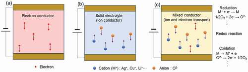
Of conductors through which charge flows in solids, as shown in , there are electronic conductors that conduct electrons and holes, solid electrolytes that conduct ions (pure ionic conductors), and mixed conductors that conduct both electrons and ions. Strictly speaking, electron holes (the lack of an electron at a position) and ion vacancies (the lack of an ion at a position) are also conduction species, but for the sake of simplicity, they are not included here. Ionic conductors and mixed conductors have either positively charged or negatively charged ions as the conducting species. Most positively charged ions are either alkali metal ions (Li+, Na+, K+), monovalent transition metal ions (Ag+, Cu+), or hydrogen ions (proton: H+). It is difficult to achieve ionic conductivity in metal ions with divalent or higher valence, due to their strong covalent nature. Negatively ionic species are oxygen ions (oxide ions: O2-) and fluorine ions (fluoride ions: F−). Electronic conductors are metals and semiconductors, and many of the devices currently in use in the information and communication fields are electronic devices that operate by utilizing the phenomena of electron transport in the materials they employ. On the other hand, solid state ionic devices operate by utilizing the phenomena of ion transport in solid electrolytes or mixed conductors. When a voltage is applied to electrodes sandwiching the solid electrolyte or mixed conductor, ions of the conducting species move along the electric field, and the electrochemical reactions of oxidation and reduction occur at interfaces with the electrodes. Many of the solid-state ionic devices in commercial use today are used in the environmental and energy sectors, including all-solid-state rechargeable batteries, fuel cells and chemical sensors. Around 1970, practical use was found for solid state ionic devices in the information and communication fields. One such was the electrochemical integrating element (Memoriode), which stored the electricity passing through them in analog form, as electrical potential [Citation25,Citation26]. However, as a result of subsequent remarkable progress in the development of semiconductor devices, solid state ionic devices for information and communications technology have almost disappeared. This is due to the fact that ions move significantly slower than electrons, which therefore slows down the operation of a device, and the presence of large numbers of ions with high mass transport, which impairs the reliability and sustainability of the device. Remarkably, recent developments in nanotechnology have made it possible to control localized ion transport. Solid state ionic devices that operate by transporting a small number of ions over nanometer. and even atomic scale distances, are being developed. Atomic scale solid state ionic device technology not only overcomes the shortcomings of conventional ionic devices in terms of operating speed and reliability but, by utilizing the structural formation and material controls associated with ion transport, is also expected to generate interesting physical and chemical phenomena that cannot be obtained with conventional electronic devices. It is for these reasons that solid state ionic devices for communication and information technology have attracted much attention over recent years.
Figure 1. Electrical conductors with various conduction species. (a): Electronic conductor transporting electrons. (b): Ionic conductors (solid electrolytes) transporting ions. (c): Mixed conductors transporting electrons and ions. In (b) and (c) conductors, electrochemical reactions of oxidation and reduction occur at the interfaces with electrodes.
3. Resistive switches using conductive metal filaments
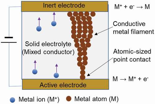
As mentioned in Section 1, it is known that atomic scale switches and the quantized conductance can be obtained by controlling the transport of a single atom or the atomic structure of a point contact using STM. Such nanoscale, and even atomic scale, control of ion transport and point contact structures, and resulting switches and quantized conductance, can be achieved easily by solid state ionic devices with simple structures [Citation27,Citation28]. The typical structure of a solid state ionic device is shown in . The device consists of a nanoscale thin film of a solid electrolyte conducting metal ions or a mixed conductor conducting metal ions and electrons, sandwiched between metal electrodes. One, the active electrode, is made of the same metal as the conducting metal ion, and the other is the inert electrode, which is made of platinum (Pt) or another material. When a negative polarity voltage is applied to the inert electrode and a positive polarity voltage is applied to the active electrode, the metal atoms of the active electrode become metal ions, through an oxidation reaction, and dissolve in the solid electrolyte or mixed conductor. The metal ions are transported through the solid electrolyte or mixed conductor and generated as metal atoms by a reduction reaction at the interface with the opposing inert electrode. As these redox reactions continue, a conductive nanoscale metal filament bridge is formed between electrodes, and the resistance between electrodes decreases rapidly. Next, when the polarity of the voltage applied between the electrodes is reversed, the metal atoms of which the metal filament is constructed become metal ions through an oxidation reaction supported by Joule heat, and are dissolved in the solid electrolyte or mixed conductor. As the reaction continues, the filament becomes thinner and thinner, and eventually breaks, which causes the resistance between the electrodes to increase rapidly. It is easy to control the point contact structure formed in the metal filament at the nanoscale, and even the atomic scale, by applying appropriate voltages for the formation and annihilation of the filament. There is also a known method of forming conductive filaments by using the transport phenomenon of oxide ions within transition metal oxides. When a voltage is applied between the electrodes sandwiching the transition metal oxide, the oxide ions, which are the conduction species, are released as oxygen gas by the oxidation reaction. As a result, oxygen vacancies are generated in the transition metal oxide and these vacancies change the valence of the transition metal, following which a conductive filament is formed by the transition metal with the changed valence. Such resistive switches, which use conductive filaments in solids, have been reported since around the 1960s [Citation29–31], but they only began to attract serious attention around the year 2000s as a result of a growing need for non-volatile, compact, and low power consumption switches and memory devices [Citation32–41].
Figure 2. Solid state ionic device consisting of a solid electrolyte conducting metal ions or a mixed conductor conducting metal ions and electrons sandwiched between inert and activated electrodes. A conductive metal filament is formed and annihilated between the electrodes by a redox reaction induced by an applied voltage.
4. Atomic switch
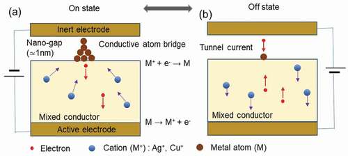
Remarkable progress has been made in the development of devices such as nonvolatile switches, resistance-change memories and memristors, which operate by controlling the structure of conductive filaments fabricated by ion transport at the nanoscale. In the future, development of atomic scale technology will be an important issue for further improving the performance and functionality of such devices. The atomic switch works by controlling the atomic structure of point contacts on the atomic scale, using the formation and annihilation of conductive filament by the transport of a small number of ions. A schematic of the structure and operation of the subject atomic switch is shown in . A mixed conductor, which conducts metal ions such as Ag+ or Cu+ and electrons, is stacked on top of a metal bottom electrode of silver (Ag) or copper (Cu). The metal electrode acts as the active electrode because a redox reaction (M (electrode) ⇆ M+(mixed conductor) + e−), M:metal atoms in electrode, M+:metal ions in mixed conductor and e−:electrons, occurs at the interface between the mixed conductor and the metal electrode. On the other hand, there is a gap between the opposing upper electrode and the mixed conductor. This upper electrode, formed from a chemically stable metal such as Pt, acts as an inert electrode. The size of the gap is about 1 nm to allow tunneling current to flow. When a voltage of negative polarity is applied to the inert electrode, the tunneling electrons from the inert electrode reduce the metal ions in the mixed conductor and produce them as metal atoms on the surface of the mixed conductor. The generation of a few metal atoms forms a conductive filament bridge between the mixed conductor and the inert electrode, which results in an On-state with low resistance ()). When the polarity of the voltage applied to the inert electrode is reversed to positive, the metal atoms constructing the bridge are ionized by the oxidation reaction and are re-dissolved into the mixed conductor. This action causes the bridge to annihilate, resulting in an Off state with high resistance ()). The atomic switch, which operates based on the principle of solid state ionics, can be said to be an atomic scale switch with a simple structure and easy operation control, which combines the features of both the atom manipulation by Eigler et al. and the point contact manipulation by Smith et al. mentioned above. As is known, the switches used in lighting fixtures operate by mechanically controlling metal contacts on the millimeter scale. The atomic switch, which is controlled in a similar way with atomic scale metal contacts, and can be described as ultimately microscopic mechanical switches.
Figure 3. Structure and operation principle of the atomic switch. The device material used is a mixed conductor that conducts metal ions and electrons. (a) On state, with a conductive metal-atom bridge. (b) Off state, without a conductive metal-atom bridge.
The basic research for the development of the atomic switch was initially conducted using STM [Citation1]. As shown in , the tip of the STM was made of Ag/Ag2S (silver sulfide) thin wire, which was prepared by sulfurizing Ag thin wire. The Ag/Ag2S-STM tip was brought close to the Pt substrate until, at about 1 nm, tunneling current was observed, and the piezoelectric position control was stopped at that position to fix the gap distance. Next, a voltage was applied to the Pt substrate by sweeping from positive to negative polarity three times. The electrical resistance at the start was a few hundred kilohms, corresponding to the tunneling resistance between the Ag/Ag2S tip and the Pt substrate. When a negative polarity voltage above the threshold was applied to the Pt substrate, a bridge was formed between the tip of the STM and the Pt electrode by the Ag atoms generated at the tip. The formation of the Ag bridge reduced the electrical resistance by about three orders of magnitude. Conversely, when the voltage was switched back to positive polarity, the silver atoms in the bridge became Ag+ by oxidation reaction and re-dissolved into the Ag2S, causing the bridge to annihilate. This also caused the electrical resistance to revert to the original tunneling resistance. By controlling these Ag bridge formation and annihilation behaviors, a switching operation could be achieved. Since the bridge structure did not change at voltages below the threshold, the On/Off state could be easily determined by applying a small voltage.
Figure 4. Resistance change between a Ag/Ag2S-STM tip and a Pt substrate after three sweeps of voltage, from positive to negative polarity. Formation and annihilation of a Ag atom bridge between the tip and the substrate occur when positive and negative polarity voltages are applied. Reproduced with permission [Citation1]. Copyright 2021, RIKEN.
![Figure 4. Resistance change between a Ag/Ag2S-STM tip and a Pt substrate after three sweeps of voltage, from positive to negative polarity. Formation and annihilation of a Ag atom bridge between the tip and the substrate occur when positive and negative polarity voltages are applied. Reproduced with permission [Citation1]. Copyright 2021, RIKEN.](/cms/asset/2f586e89-9fde-4b49-bed2-ea5799ce8da9/tapx_a_2065217_f0004_oc.jpg)
It is interesting to see how fast an atomic switch that operates by ion transport compared to a conventional semiconductor switch, which operates by electron transport. In order to correctly determine such speed, switch times and behaviors have been examined using STM tips made from various mixed conductors [Citation42–49]. Valov et al. have measured switch times using a stacked substrate of Ag and iron (Fe)-doped rubidium silver iodide (RbAg4I5) films and a Pt-STM tip [Citation47]. RbAg4I5 is a solid electrolyte that conducts Ag+, but when doped with Fe, it has the property of a mixed conductor of Ag+ and electrons. shows the relationship between time and the current flowing between the STM tip and the substrate due to the application of voltage. In region ①, a voltage of +100 mV was applied to the Pt tip, and no increase in current was observed over time because no silver atoms were generated by the reduction reaction of Ag+ in RbAg4I5. Next, a voltage of −100 mV was applied to the Pt tip. Immediately after that, in region ②, almost no current change was observed. In region ③, where a little time had passed, Ag+ in RbAg4I5 started to be generated as silver atoms by a reduction reaction, and the current increased rapidly. After more time passed, a Ag atom bridge was formed between the tip and the substrate. At this initial stage of region ④, the quantized conductance of the basic unit (G0) was measured by a point contact between a single Ag atom and the tip. In region ④, where further time had passed, a stepwise current increase was observed due to a state change of the quantized conductance (N·G0: N = 1, 2, 3 …) because of the increase in the number of atoms of which the point contact was constituted. Eventually, in region⑤, as the area of the point contact increased further, the current reached a maximum value that was limited by the external reference resistance. shows the relationship between applied voltage and switching time in semi-logarithmic coordinates. The switch time was determined by the time it took for a single Ag atom to make point contact with the STM tip when a pulse voltage of a magnitude between −75 mV and −600 mV was applied to the STM tip at room temperature. In other words, it was determined by measuring the time it took to change from the off state of the tunnel resistance to the on state of the quantized conductance G0. As the applied voltage increased, the switch time decreased exponentially. The slope was clearly separated into two regions: a region for applied voltages of between −75 mV and −300 mV and a region for applied voltages of between −300 mV and −600 mV. The corresponding reciprocal slopes were calculated to be b1 = 21 mV and b2 = 125 mV. This argues for switch time (ts) being determined by the nucleation rate associated with the reduction of Ag+ in RbAg4I5, and derives the numerical expression (1) for ts according to the atomistic model for electrocrystallization [Citation50,Citation51].
Figure 5. Relationship between current and time at applied voltages of 100 mV and −100 mV. The numbers (①-⑤ are five regions divided by current and time characteristics, which correspond to the process of bridge formation by Ag atoms shown in the upper part of the graph. About four Ag atoms are required to make a bridge in a gap of approximately 1 nm. The inset shows the first quantum conductance step at G0. Reproduced with permission [Citation47]. Copyright 2012, Springer Nature.
![Figure 5. Relationship between current and time at applied voltages of 100 mV and −100 mV. The numbers (①-⑤ are five regions divided by current and time characteristics, which correspond to the process of bridge formation by Ag atoms shown in the upper part of the graph. About four Ag atoms are required to make a bridge in a gap of approximately 1 nm. The inset shows the first quantum conductance step at G0. Reproduced with permission [Citation47]. Copyright 2012, Springer Nature.](/cms/asset/05b33cba-9cb3-4b9b-b6e4-56ba25a315e4/tapx_a_2065217_f0005_oc.jpg)
Figure 6. Relationship between switching time (ts) and applied voltage (Δφ). The switching time was determined by measuring the time to change from the off state of the tunnel resistance to the on state of the quantized conductance G0. Reproduced with permission [Citation47]. Copyright 2012, Springer Nature.
![Figure 6. Relationship between switching time (ts) and applied voltage (Δφ). The switching time was determined by measuring the time to change from the off state of the tunnel resistance to the on state of the quantized conductance G0. Reproduced with permission [Citation47]. Copyright 2012, Springer Nature.](/cms/asset/fd6d29d6-2a68-43d7-8ea3-f6f872bb6692/tapx_a_2065217_f0006_oc.jpg)
where k is the Boltzmann constant, T is temperature, α is the transfer coefficient, t0 is a constant, Δφ is voltage and Nc is the number of atoms constituting the critical nucleus. This elementary formation process of one or several Ag atoms on the RbAg4I5 surface can be described as nucleation by electrochemical reaction limited to the initial stage that occurs via ion transport by voltage application. It also explains that the cause of the two regions with different slopes is due to the difference in Nc. Nc = 1 has a physical meaning where each Ag atom generated on the RbAg4I5 surface is considered to be a nucleus of the new phase. Nc = 0 means that the empty nucleation site acts sannka s the critical nucleus and that the single Ag atom generated represents the supercritical cluster of the new phase. Using the same technique as in , metal nuclei have been found to grow on the surface of metal oxides with migrating oxygen vacancies [Citation48,Citation49].
Krishnan et al. have investigated the relationship between the atomic structure of the point contact made by a conducting Ag filament in a electrolyte and quantized conductance using first-principles DFT calculations [Citation52,Citation53]. The ideal Ag atom structures for point contacts built in the Ag atom filament were assumed to be 1, 2, 3, 4 and 9 atom chain structures, as shown in ). The conduction channels consisted of repeats of these atomic chains, which were connected to the electrodes on both sides.
Figure 7. (a) Atomic structures of the point contacts of a Ag filament, assuming chain structures consisting of 1, 2, 3, 4, and 9 atoms. (b) Relationship between quantized conductance and electron energy in various point contact chain structures. Reproduced with permission [Citation52]. Copyright 2017, John Wiley and Sons.
![Figure 7. (a) Atomic structures of the point contacts of a Ag filament, assuming chain structures consisting of 1, 2, 3, 4, and 9 atoms. (b) Relationship between quantized conductance and electron energy in various point contact chain structures. Reproduced with permission [Citation52]. Copyright 2017, John Wiley and Sons.](/cms/asset/fbc25aa9-0c8a-4795-afc7-95d733919770/tapx_a_2065217_f0007_oc.jpg)
) shows the relationship between the conductance and the electronic energy in the structure of each atomic chain, as estimated by calculation. The conductance was plotted with respect to the basic unit of quantized conductance (Go), and the electron energy with respect to the Fermi energy (Ef) of the equilibrium state. At electron energies of around 1 eV, the conductances of the atomic structures of the 1, 2, 3, 4 and 9 atomic chains were estimated to be quantized states of 1G0, 2G0, 3G0, 4G0 and 9G0, respectively.
In conductive filaments formed with various solid electrolytes and mixed conductors, the conductance resulting from point contacts does not always show integer multiple values with respect to the basic unit of quantized conductance. It has also been reported to show values such as half-integer multiples and fractional values of G0. In order to theoretically elucidate the cause of this, the quantized conductance of point contacts with rather complex atomic structures have also been estimated by first principles DFT calculations. As shown in ), each point contact structure of the conduction channel was assumed to consist of 10, 11 and 12 Ag atoms respectively. The relationship between conductance and electron energy for each point contact is shown in ). In the single-atom point-contact structure with a 10 atom chain, the electronic energy was almost 1G0 around Ef. This is completely governed by the single-atom point contact, and hence a transmission rate at almost full unity is achieved. On the other hand, the point contact structure consisting of two atoms (11- and 12-atom chains) showed conductance values lower and higher than 2G0 around Ef, respectively. These point contact structures are heavily twisted and lose their translational invariance along channels. Therefore, the electrons in the individual conduction channels were considered to undergo intense elastic scattering. These theoretical calculations showed that the conductance of an atomic scale point contacts is strongly influenced by their atomic configurations, and a small disturbance of the atomic arrangement of an atomic point contact changes the quantized conductance by a half-integer or fractional factor. The quantized conductance is also disturbed by the adsorption of impurities such as a hydrogen, oxygen or hydroxide on the point contacts [Citation54].
Figure 8. (a) Atomic structures of point contacts of a Ag filament, assuming slightly twisted chain structures consisting of 10, 11 and 12 atoms. (b) Relationship between quantized conductance and electron energy in various slightly twisted point contact chain structures. Reproduced with permission [Citation52]. Copyright 2017, John Wiley and Sons.
![Figure 8. (a) Atomic structures of point contacts of a Ag filament, assuming slightly twisted chain structures consisting of 10, 11 and 12 atoms. (b) Relationship between quantized conductance and electron energy in various slightly twisted point contact chain structures. Reproduced with permission [Citation52]. Copyright 2017, John Wiley and Sons.](/cms/asset/b1d7e105-73ac-4d04-88ad-b9282ce04cdd/tapx_a_2065217_f0008_oc.jpg)
5. Device applications
Based on basic experiments with atomic switches using STM, practical devices have been developed using conventional microfabrication techniques [Citation2]. ) (b) are scanning electron micrographs of an atomic switch constructed by the microfabrication method and the fabrication procedure, respectively. The atomic switch with the Pt top electrode/Ag/Ag2S/Ag bottom electrode stacked structures was fabricated on a silicon wafer using a lithographic technique, such as electron beam lithography, metal deposition and lift-off. The Ag layer between the Pt top electrode and the Ag2S layer was about 1 nm thick. When a negative voltage of appropriate magnitude was applied to the Ag bottom electrode between the Pt and Ag electrodes, the 1 nm thick Ag layer was dissolved into the Ag2S layer by oxidation reaction, and a gap of about 1 nm was formed between the Pt top electrode and the Ag2S layer. The resistance of the gap through which the tunneling current flows was large, which is the off-state. When a voltage with a positive polarity was applied to the Ag bottom electrode, a conductive Ag bridge was formed between the Pt top electrode and the Ag2S layer due to the reduction of Ag+ in Ag2S by tunneling electrons, which is the on-state. Atomic switches can be fabricated using the microfabrication techniques used to fabricate semiconductor devices, and can therefore be integrated into conventional semiconductor circuits.
Figure 9. (a) Scanning electron micrograph of an atomic switch constructed by a microfabrication method. (b) Schema of the fabrication procedure. Reproduced with permission [Citation2]. Copyright 2005, Springer Nature.
![Figure 9. (a) Scanning electron micrograph of an atomic switch constructed by a microfabrication method. (b) Schema of the fabrication procedure. Reproduced with permission [Citation2]. Copyright 2005, Springer Nature.](/cms/asset/a279a299-31cf-494b-818a-6270f29ea8d4/tapx_a_2065217_f0009_oc.jpg)
Atomic switches have the potential to realize a wide variety of functionalities. By combining two atomic switches, it is possible to construct a logic circuit, which is the basis of computer hardware. ) (b) (c) show the structures of basic AND, OR and NOT logic gates that were constructed using atomic switches, and the results of their experimental operation, respectively. The input signals were judged as the logical value 1 when the voltage was applied to input 1 or 2, and as the logical value 0 when voltage was not applied. The output signals were then judged to be 1 when voltage was detected, and 0 when no voltage was detected. Depending on the applied voltage at input 1 or input 2, Ag atom bridges were formed or annihilated at the respective atomic switches. The AND gate shown in ) was formed as a crossbar structure of one mixed conductor Ag2S wire and two Pt wires. The output voltage was only detected when voltages were applied to both inputs 1 and 2. In an OR gate formed by two Ag2S and one Pt wire ()), the absence of output voltage was only detected when no voltage was applied to either of the two inputs. The NOT gate detected the output voltage when there was no input voltage, and did not detect the output voltage when there was an input voltage ()). It is possible to construct various logic operation circuits by combining said basic AND, OR and NOT logic gates.
Figure 10. Basic logic gates fabricated by atomic switches and their operation. (a) AND gate. (b) OR gate. (c) NOT gate. Reproduced with permission [Citation2]. Copyright 2005, Springer Nature.
![Figure 10. Basic logic gates fabricated by atomic switches and their operation. (a) AND gate. (b) OR gate. (c) NOT gate. Reproduced with permission [Citation2]. Copyright 2005, Springer Nature.](/cms/asset/9e18ce3e-8885-48d2-b1fa-e6512022cfb6/tapx_a_2065217_f0010_oc.jpg)
Figure 11. Switching of quantized conductance states using a two-atom switch system with a crossbar structure consisting of two Pt wires and one Ag2S/Ag wire. N1 and N2 is the quantized conductance state of two atomic switches, respectively. Ntotal is the total quantized-conductance state of the system. Reproduced with permission [Citation2]. Copyright 2005, Springer Nature.
![Figure 11. Switching of quantized conductance states using a two-atom switch system with a crossbar structure consisting of two Pt wires and one Ag2S/Ag wire. N1 and N2 is the quantized conductance state of two atomic switches, respectively. Ntotal is the total quantized-conductance state of the system. Reproduced with permission [Citation2]. Copyright 2005, Springer Nature.](/cms/asset/9d03741b-aa18-4977-9918-f909bfba6ba7/tapx_a_2065217_f0011_oc.jpg)
It is also possible to construct an adder circuit of quantized conductance using atomic switches. In STM experiments, it was found that states of the quantized conductance (N·Go: N = 0, 1, 2, 3 …) can be switched by precisely controlling the position of the STM tip and the applied voltage. In an atomic switch device, the number of Ag atoms in point contact of the bridge was also controlled through the use of redox reactions induced by the application of appropriate pulsed voltages. By controlling the atomic structure of the point contact, each state of the quantized conductance could be reversibly switched. Here, two atomic switches with nanogaps were constructed using a crossbar structure of two Pt wires and one Ag2S/Ag wire (). By applying appropriate pulsed voltages at room temperature, the quantized conductance of the two atomic switches formed at each intersection could be independently controlled in a stepwise manner, in integer multiples of N = 0 to 3. The total conductance, calculated from the total current measured at the end of the Ag2S/Ag wire, corresponded to the sum of the two quantized conductances, suggesting that this system of two atomic switches acts as an adder circuit. With two semiconductor switches indicating the On/Off state, only 2 × 2 = 4 states can be created, but with two atomic switches, at least 4 × 4 = 16 states can be created. This shows that it is possible to build high-performance circuits, with multiple memory functions, by using multiple atomic switches.
The resistance of the atomic switch changes significantly, by more than three orders of magnitude from a large value to a small value, when a voltage is applied. This is due to the change from uncontacted to point contact on the atomic scale and then to point contact on the nanoscale as the metal bridge grows. The size of the area of the point contact can be controlled by the number of times the appropriate pulse voltage is applied. Based on the idea that the pulsed voltage-induced process of growth of a bridge in an atomic switch is similar to the process of growth of nerve cells in the brain induced by learning, a neuromorphic device has been developed, with a learning function that uses an atomic switch [Citation55,Citation56]. An atomic switch will have a learning memory function by analog resistance change if the bridge size is controlled at the nanoscale, but will have a memory function by digital resistance change using several quantized states if the bridge size is controlled at the atomic scale.
Conductance control of a quantized atomic switch has been demonstrated, but further work is needed to commercialize such a device. For example, at the present stage, as the state number (N) of the quantized conductance increases, the state control at the larger number becomes more difficult. Even when N is small, some switches have less control over some quantization state values, such as half-integer multiples. This is because quantized conductance is strongly related to atomic structure, stability and reproducibility of the point contact, which are still difficult to control. Therefore, further improvements in the materials used to fabricate, and structures of, the atomic switch are essential if the practical application of quantized conductance devices is to be achieved.
Another type of quantized conductance switches has also been developed, in which the atomic structures of point contacts of a conducting filaments are controlled without using tunneling currents. Said devices have simple structures that consist of solid electrolytes or mixed conductors, such as sandwiched between electrodes. Quantized conduction properties generated using the conduction of metal ions or oxygen ions in materials such as tantalum oxide [Citation57,Citation58], zinc oxide [Citation59], hafnium oxide [Citation60,Citation61], germanium sulfide [Citation62], silicon oxide [Citation63] and silver iodide [Citation64,Citation65] have been reported. By precisely controlling the applied voltage and current, the state of the quantized conductance is switched. As an example, a device with a structure of tantalum oxide (Ta2O5) sandwiched between Ag and Pt electrode, as shown in ), is presented. By gradually increasing the magnitude of the positive polarity pulse voltage applied to the Ag electrode, while limiting the current, the quantized conductance states were switched stepwise from N = 0 to 9 by increasing the point contact area of the Ag bridge at the atomic scale. Immediately after application of the pulsed voltage, there were temporary significant increases in conductance, which were due to the instability of the atomic structure of the point contact. The conductance then stabilized with a transition to stable structures. The polarity of the pulse voltage applied to the Ag electrode was then reversed to negative. By gradually increasing the magnitude of the applied voltage, the area of the point contact was reduced on an atomic scale and the states of the quantized conductance were switched stepwise from N = 9 to 0. Point contacts constructed on the principle of solid-state ionics are affected by ion transport and electrochemical reactions consequent to the application of voltage. Therefore, in order to stably control quantized conduction, it is necessary to find the optimal conditions for constructing point contacts, This is done by examining the combined factors that affect solid-state electrochemical phenomena such as the voltage-current application process, the type of conducting ions, ion concentration and conductivity, the composition and crystal structure of ion conductors, and impurities such as water.
Figure 12. (a) Increase in the quantized conductance states in a Ag/Ta2O5/Pt device as a result of applying positive pulse voltage to the Ag electrode. (b) Decrease in the quantized conductance states as a result of applying negative pulse voltage to the Ag electrode. Reproduced with permission [Citation57]. Copyright 2012, IOP.
![Figure 12. (a) Increase in the quantized conductance states in a Ag/Ta2O5/Pt device as a result of applying positive pulse voltage to the Ag electrode. (b) Decrease in the quantized conductance states as a result of applying negative pulse voltage to the Ag electrode. Reproduced with permission [Citation57]. Copyright 2012, IOP.](/cms/asset/70977897-d99e-4c26-a41f-17b0c562bc56/tapx_a_2065217_f0012_oc.jpg)
Memristors, which store the amount of charge flowing and change their resistance value accordingly, have attracted much attention in recent years [Citation66]. Some memristors operate on the same principle as the atomic switch, using the formation and annihilation of conductive filaments. In one application for memristors, they are expected to act as artificial synapses at the cross-points of crossbar structures working as hierarchical neural networks [Citation67–74]. The weight control of the signal transmission is based on a reversible change in resistance, which depends on the area of the point contact of the filament. Precise control in such device is not easy to achieve, however, if the atomic structure of a point contact can be precisely controlled, it may be possible to realize an ultra-fine artificial synapse using quantized conductance.
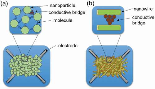
The aforementioned atomic scale switches are mainly composed of layers of thin films, but atomic scale switches that use low-dimensional materials such as nanoparticles and nanowires have also been reported [Citation12,Citation75–88]. ) shows a switch device with a huge number of nanoparticles self-assembled on a substrate [Citation75–79]. By using nanoparticles with molecules and other substances adsorbed on their surfaces, the spacing between nanoparticles can be kept uniform to the level of a few nanometers. By applying voltage from electrodes, conductive bridges are formed between nanoparticles by ion transport along the electric field and electrochemical reactions or by atom transport via electric-field-induced evaporation. Depending on the conditions of the applied voltage, point contacts with conductive bridges are formed at various locations, creating complex networks of percolating nanostructures. ), on the other hand, shows a switch device with a huge number of nanowires self-assembled on a substrate [Citation80–88]. In a manner that is similar to what is observed with self-assembled nanoparticles, nanophenomena such as ion transport along electric fields and electrochemical reactions occur when voltage is applied from electrodes, forming conductive bridges between nanowires. Depending on the applied voltage conditions, complex networks of percolating nanostructures are constructed by the formation of point contacts with conductive bridges at various locations. In addition to possessing switching properties, these complex networks of nanoparticles and nanowires also possess other interesting properties, such as nonlinear electrical and memristor properties. Such properties are expected to be used to develop neuromorphic devices with synaptic and other functions, and for developing other devices for reservoir computers. Furthermore, these nanoparticle- and nanowire-based atomic scale switches have several advantages, including not requiring complex fabrication equipment, an ability to be constructed with simple processes and being able to operate neural circuits with a relatively small number of electrodes.
Figure 13. Atomic scale switch networks fabricated using (a) self-assembled nanoparticles, and (b) self-assembled nanowires.
6. Conclusion
Atomic scale switches based on the principle of solid-state ionics, using ion transport and electrochemical phenomena, are promising future nanodevices due to their simple structures, ease of control and other properties. By using quantized conductance, it is possible to fabricate devices and circuits with various functions. Switches of this sort, represented by the atomic switch, can be constructed using conventional microfabrication techniques, and operate efficiently at room temperature and in air. As such, they can be incorporated into current semiconductor integrated circuits so as to overcome the performance limitations of conventional circuits. In addition, atomic scale switches with synaptic functions based on quantized conductance are expected to be part of the architecture of new types of in-memory computers that are small in size and consume less power.
Disclosure statement
No potential conflict of interest was reported by the author(s).
References
- Terabe K, Hasegawa T, Nakayama T, et al. Quantum point contact switch realized by solid electrochemical reaction. Riken Rev. 2001;37:7–24.
- Terabe K, Hasegawa T, Nakayama T, et al. Quantized conductance atomic switch. Nature. 2005;433:47–50.
- Hasegawa T, Terabe K, Sakamoto T, et al. Nanoionics switching devices: Atomic switches. MRS Bull. 2009;34:929–934.
- Hino T, Hasegawa T, Terabe K, et al. Atomic switch: atomic-movement-controlled nanodevices for new types of computing. Sci Tech Adv Mater. 2011;12:013003.
- Hasegawa T, Terabe K, Tsuruoka T, et al. Atomic switch: Atom/ion movement controlled devices for beyond von-Nuemann computers. Adv Mater. 2012;24:252–267.
- Terabe K, Hasegawa T, Nakayama T, et al. Atomic switch - from invention to practical use and future prospect. In: Invention and development of atomic switch Aono, Masakazu. Switzerland: Springer, 2020. 1–16. 978-3-030-34874-8 doi:10.1007/978-3-030-34875-5.
- Kudo T, Fueki K. Solid state ionics. Germany: VCH Weinheim; 1990. 978-0895739858.
- Takahashi T. Solid state ionics - Recent trends and future expectations. Bull. Electrochem. 1995;11:1–33.
- Knauth P, Tuller HL. Solid-state ionics: Roots, status, and future prospects. J Am Ceram Soc. 2002;85:1654–1680.
- Terabe K, Hasegawa T, Liang C, et al. Control of local ion transport to create unique functional nanodevices based on ionic conductor. Sci. Tech. Adv. Mater. 2007;8:536–542.
- Terabe K, Tsuchiya T, Yang R, et al. Nanoionics devices enabling a multitude of new features. Nanoscale. 2016;8:13873–13879.
- Terabe K, Tsuchiya T, Tsuruoka T. A variety of functional devices realized by ionic nanoarchitectonics, complementing electronics components. Adv Electron Mater. Early view. 2021. Doi: 10.1002/aelm.202100645
- Eigler DM, Lutz CP, Rudge WE. An atomic switch realized with the scanning tunneling microscope. Nature. 1991;352:600603.
- Smith DPE. Quantum point contact switches. Science. 1995;269:371–373.
- Gimzewski JK, Möller R. Transition from the tunneling regime to point contact studied using scanning tunneling microscopy. Phys Rev B. 1987;36:1284–1287.
- Agraït N, Rodrigo JG, Vieira S. Conductance steps and quantization in atomic-size contacts. Phys Rev B. 1993;47:12345–12348.
- Krans JM, Muller CJ, Yanson IK, et al. One-atom point contacts. Phys Rev B. 1993;48:14721–14724.
- Pascual JI, Méndez J, Gómez-Herrero J, et al. Quantum contact in gold nanostructures by scanning tunneling microscopy. Phys Rev Lett. 1993;71:1852–1855.
- Olesen L, Lægsgaad E, Stensgaad I, et al. Quantized conductance in an atom-sized point contact. Phys Rev Lett. 1994;72:2251–2254.
- Pascual JI, Méndez J, Gómez-Herrero J, et al. Properties of metallic nanowires: From conductance quantization to localization. Science. 1995;267:1793–1795.
- Krans JM, van Ruitenbeek JM, Fisun VV, et al. The signature of conductance quaintization in metallic point contacts. Nature. 1995;375:767–769.
- Ohnishi H, Kondo Y, Takayanagi K. Quantized conductance through individual rows of suspended gold atom. Nature. 1998;395:780–783.
- van Wees BJ, van Houten H, Beenakker CW, et al. Quantizes conductance of point contacts in a two-dimensional electron gas. Phys Rev Lett. 1998;60:848–850.
- Wharam DA, Thoronton TJ, Newbury R, et al. One-dimensional transport and the quantisation of the ballistic resistance. J Phys C. 1998;21:L209.
- Takahashi T, Yamamoto O. Solid state ionics- The electrochemical analog memory cell with solid electrolyte. J Appl Electrochem. 1973;3:129–135.
- Tada K, Ikeda H. Sanyo’s couliodes and memoriodes, in: applications of Solid Electrolytes. Takahashi T, Kozawa A, Eds. Cleveland: JEC Press, US Office of the Electro-chemical Society of Japan; 1980. p. 40–45.
- von Ruitenbeek JM, Masis MM, Miranda E. Quantum point contact conduction Ielmini , Daniele, Waser, Rainer. Resistive switching : From Fundamentals of nanoionic redox processes to memristive device applications (Germany: Wiley-VCH). 2016;197–223. 978-3-527-33417-9.
- Xue W, Gao S, Shang J, et al. Recent advanced of quantum conductance in memristor. Adv Electron Mater. 2019;5:1800854.
- Hickmott TW. Low-frequency negative resistance in this anodic oxide films. J Appl Phys. 1962;33:2669–2682.
- Gibbons JF, Beadle WE. Switching properties of thin NiO films. Solid-state Electro. 1964;7:785–797.
- Hirose Y, Hirose H. Polarity-dependent memory switching and behavior of Ag dendrite in Ag-photodoped amorphous As2S3 films. J Appl Phys. 1976;47:2767–2772.
- Kozicki MN, Park M, Mitkova M. Nanoscale memory elements based on solid-state electrolytes. IEEE Trans Nanotechnology. 2005;4:331–338.
- Waser R, Aono M. Nanoionics-based resistive switching memories. Nat Mater. 2007;6:833–840.
- Sawa A. Resistive switching in transition metal oxides. Mater Today. 2008;11:28–36.
- Akinaga A, Shima H. Resistive random access memory (ReRAM) based on metal oxide. Proc IEEE. 2010;98:2237–2251.
- Wong HSP, Lee LH, Yu SM, et al. Metal-oxide RRAM, Proc. IEEE. 2012;100,1951–1966 doi:10.1109/JPROC.2012.2190369.
- Pan F, Gao S, Chen C, et al. Recent progress in resistive random access memories: Materials, switching mechanism, and performance. Mater Sci Eng. 2014; 83:1–59. R.
- Wouters DJ, Waser R, Wuttig M. Proc. IEEE. 2015;103:1274–1288.
- Valov I, Luebben M, Wedig A, et al. Mobile ion, transport and redox processes in memristive devices. ESC Trans. 2016;75:27–39.
- Kozicki MN, Volov I. Electrochemical metallization memories Ielmini, Daniele, Waser, Rainer. Resistive switching, From fundamentals of nanoionic redox processes to memristive device application. Germany: Wiley-VCH; 2016. p. 483–513.
- Dash CS, Prabaharan SRS. Nano resistive memory (Re-RAM) devices and their applications. Rev Adv Mater Sci. 2019;58:248–270.
- Tamura T, Hasegawa T, Terabe K, et al. Switching property of atomic switch controlled by solid electrochemical reaction. Japan J Apply Phys. 2006;45:L364–366.
- Tamura T, Hasegawa T, Terabe K. Materials dependence of switching speed of atomic switches made from silver sulfide and from copper sulfide. J Phys Conf Ser. 2007;61:1157–1161.
- Nayak A, Tamura T, Tsuruoka T, et al. Rate-limiting processes determining the switching time in a Ag2S atom switch. J Phys Chem Lett. 2010;1:604–608.
- Nayak A, Tsuruoka T, Terabe K. Switching kinetics of a Cu2S-based gap-type atomic switch . Nanotechnology. 2011;22:235201.
- Morales-Masis M, van der Molen SJ, Hasegawa T, et al. Bulk and surface nucleation processes in Ag2S conductance switches. Phys Rev B. 2011;84:115310.
- Valov I, Sapezanskaia I, Nayak A, et al. Atomically controlled electrochemical nucleation at superionic solid electrolyte surfaces. Nat Mater. 2012;11:530–535.
- Wedig A, Luebben M, Y CD, et al. Nanoscale cation motion in TaOx, HfOx and TiOx memristive systems. Nature Nanotechnology. 2016;11:67–75.
- Moors M, K AK, Lu Q, et al. Resistive switching mechanisms on TaOx and SrRuO3 thin-film surfaces probed by scanning tunneling microscopy. ACS Nano. 2016;10:1481–1492.
- Budevski E, Staikov G, Lorenz WJ. Electrocrystallization: Nucleation and growth phenomena. Electrochim Acta. 2000;45:2559–2579.
- Milchev A. Electrocrystallization: Fundamentals of nucleation and growth. Russian J. Electrochemistry. 2008;44:619–645.
- Krishnan K, Muruganathan M, Tsuruoka T, et al. Highly reproducible and regulated conductance quantization in a polymer-based atomic switch. Adv Funct Mater. 2017;27:1605104.
- Krishnan K, Muruganathan M, Tsuruoka T, et al. Quantized conductance operation near a single-atom point contact in polymer-based atomic switch. Japan J Appl Phys. 2017;56:06GF02.
- Thygesen KS, Bollinger MV, Jacobsen KW. Conductance calculation with a wavelet bias set. Phys Rev B. 2003;67:115404.
- Ohno T, Hasegawa T, Tsuruoka T, et al. Short-term plasticity and long-term potentiation mimicked in single inorganic synapses. Nat Mater. 2011;10:591–595.
- Hasegawa T, Ohno T, Terabe K, et al. Learning abilities achieved by a single solid-state atomic switch. Adv Mater. 2010;22:1831–1834.
- Tsuruoka T, Hasegawa T, Terabe K, et al. Conductance quantization and synaptic behavior in a Ta2O5 based atomic switch. Nanotechnology. 2012;23:435705.
- Sahu VK, Misra P, K DA, et al. Quantized conductance in Ta2O5 based resistive random access memory device. AIP Conf Proc. 2017;1832:120026.
- Zhu X, Su W, Liu Y, et al. Observation of conductance quantization in oxide-based resistive switching memory. Adv Mater. 2012;24:3941–3946.
- Aga FG, Woo J, Song J, et al. Controllable quantized conductance for multilevel data storage application using conductive bridge random access memory. Nanotechnology. 2017;28:115707.
- Banerjee W, Hwang H. Quantized conduction device with 6-bit storage based on electrically controlled break junction. Adv Electron Mater. 2019;5:1900744.
- Jameson JR, Gilbert N, Koushan F, et al. Quantized conductance in Ag/GeS2/W conductive-bridge memory cells. IEEE Electron Device Lett. 2012;33:257–259.
- Nandakumar SR, Minvielle M, Nagar S, et al. A 250 mV Cu/SiO2/W memrister with half-integer quantum conductance states. Nano Lett. 2016;16:1602–1608.
- Tappertzhofen S, Valov I, Waser R. Quantum conductance and switching kinetics of AgI-based microcrossbar cells. Nanotechnology. 2012;23:145703.
- Jiang L, Xu L, Chen JW, et al. Conductance quantization in an AgInSbTe-based memristor at nanosecond scale. Appl Phys Lett. 2016;109:153506.
- Strukov DB, Snider GS, Stewart DR, et al. The missing memristor found. Nature. 2008;453:80–83.
- Lai Q, Zhang L, Li Z, et al. Ionic/electronic hybrid materials integrated in a synaptic transistor with signal processing and learning function. Adv Mater. 2010;22:2448–2453.
- Jo SH, Chang T, Ebong I, et al. Nanoscale memristor device as synapse in neuromorphic systems. Nano Lett. 2010;10:1297–1301.
- Yang R, Terabe K, Liu G, et al. On-demand nanodevice with electrical and neuromorphic multifunction realized by local ion migration. ACS Nano. 2012;6:9515–9521.
- Edwards AH, Barnaby HJ, Campbell KA, et al. Reconfigurable memristive device technology. Proc. IEEE. 2015;103:1004–1033.
- Zidan M, Strachan J, Lu W. The future of electronics based on memristive systems. Nature Electron. 2018;1:22–29.
- Tang J, Yuan F, Shen X, et al. Bridging biological and artificial neural networks with emerging neuromorphic devices: fundamentals, progress, and challenges. Adv Mater. 2019;31:1902761.
- Li Y, Lu J, Shang D, et al. Oxide-based electrolyte-gated transistors for spatiotemporal information processing. Adv Mater. 2020;32:2003018.
- Li Y, Xuan Z, Lu J, et al. One transistor one electrolyte-gated transistor based spiking neural network for power-efficient neuromorphic computing system. Adv Funct Mater. 2021;31:2100042.
- Yin S, Terabe K, Toney MF, et al. Effect of sintering condition on mixed ionic-electronic conducting properties of silver sulfide nanoparticles. J Appl Phys. 2012;111:053530.
- Bose SK, Lawrence CP, Liu Z, et al. Evolution of a designless nanoparticle network into reconfigurable boolean logic. Nat Nanotechnol. 2015;10:1048–1053.
- Mallinson JB, Shirai S, Acharya AK, et al. Avalanches and criticality in self-organized nanoscale networks. Sci Adv. 2019;5:eaaw8438.
- Bose SK, Shirai S, Mallinson JB, et al. Synaptic dynamics in complex self-assembled nanoparticle networks. Faraday Discuss. 2019;213:471–485.
- Pike MD, Bose SK, Mallinson JB, et al. Atomic scale dynamics drive brain-like avalanches in percolating nanostructured networks. Nano Lett. 2020;20:3935–3942.
- Avizienis AV, Sillin HO, Martin-Olmos C, et al. Neuromorphic atomic switch networks. PLoS One. 2012;7:e42772.
- Stieg AZ, Avizienis AV, Silin HO, et al. Emergent criticality in complex turning B-type atomic switch networks. Adv Mater. 2012;24:286–293.
- Sillin HO, Aguilera R, Shieh HHS, et al. A theoretical and experimental study of neuromorphic atomic switch networks for reservoir computing. Nanotechnology. 2013;24:384004.
- Milano G, Luebben M, Ma Z, et al. Self-limited single nanowire systems combining all-in-one memristive and neuromorphic functionalities. Nature Commun. 2018;9:5151.
- Milano G, Boarino L, Ricciardi C. Junction properties of single ZnO nanowires with asymmetrical Pt and Cu contacts. Nanotechnology. 2019;30:244001.
- Miranda E, Milano G, Ricciardi C. Compact modeling of the I-V characteristics of ZnO nanowires including nonlinear series resistance effects. IEEE Trans Nanotechnology. 2020;19:297–300.
- Kuncic Z, Nakayama T. Neuromorphic nanowire networks: Principles, progress and future prospects for neuro-inspired information processing. Adv Phys X. 2021;6:1894234.
- Loeffler A, Zhu R, Hochstetter J, et al. Topological properties of neuromorphic nanowire networks. Frontiers Neurosci. 2020;14:184.
- Hochstetter J, Zhu R, Loeffler A, et al. Avalanches and edge-of chaos learning in neuromorphic nanowire networks. Nature Commun. 2021;12:4008