
 ?Mathematical formulae have been encoded as MathML and are displayed in this HTML version using MathJax in order to improve their display. Uncheck the box to turn MathJax off. This feature requires Javascript. Click on a formula to zoom.
ABSTRACT
Group III–V semiconductors are based on the elements of groups III and V of the periodic table. The possibility to grow thin-films made of binary, ternary, and quaternary III–V alloys with different fractions of their constituent elements allows for the precise engineering of their optical properties. In addition, since many III–V compounds are direct-bandgap semiconductors, they are suitable for the development of photonic devices and integrated circuits, especially when monolithic integration is required. Moreover, the strong optical nonlinearities of III–V materials enable a fertile field of research in photonic devices for all-optical signal processing, wavelength conversion, and frequency generation. Experimentally accessing the plethora of nonlinear optical phenomena in these materials considerably facilitates the exploration of light-matter interactions. Several demonstrations have explored the optical nonlinearities in waveguides, microring resonators, photonic crystal structures, quantum dots, and lasers. In this review, we survey numerous nonlinear optical studies performed in III–V semiconductor waveguide platforms. In particular, we discuss linear and nonlinear optical properties, material growth and fabrication processes, newer hybrid material platforms, and several nonlinear optical applications of III–V semiconductor integrated optical platforms.
Graphical abstract
1. Introduction
Photonics enables the generation, processing, and detection of light by means of specially designed micro- and nano-structures. Facilitated by recent developments in nanofabrication technologies, there has been a revolution in the field of integrated photonics, in which many functionalities of a free-space optical setup with bulk components can be down-scaled onto an optical chip as small as [Citation1]. Nonlinear photonics, in particular, is a field where the high-intensity regime required for nonlinear optical experiments and applications is readily achieved in photonic devices due to the tight light confinement featured by such structures.
Photonic devices have been demonstrated on a variety of material platforms, such as metals, insulators, polymers, and semiconductors [Citation2–4]. The first nonlinear optical processes were demonstrated in the III–V semiconductors GaAs and AlGaAs in the 1970s and 1980s [Citation5–7]. In the 1990s, the nonlinear photonics research in AlGaAs devices expanded considerably [Citation8–43]alongside with the development of nonlinear photonics in InP, another III–V material [Citation44–49]. Then, in an aim to adapt the fabrication techniques, facilities, and supply chain of the microelectronics industry to photonics, nonlinear photonics in the silicon-on-insulator (SOI) platform gained considerable attention in the 2000s [Citation50–53]. However, there are some drawbacks of using silicon platforms in photonics, such as degraded performance at high temperatures [Citation54], indirect bandgap [Citation55], centro-symmetric crystal structure inhibiting second-order nonlinear optical interactions [Citation56], and the difficulty of true monolithic integration in the mid-infrared region [Citation57]. Nonlinear photonics in SOI, in particular, also suffers from strong two-photon (2PA) and free-carrier (FCA) absorption in the wavelength range below [Citation58,Citation59], leading silicon-based photonics to explore compatible alternatives like silicon nitride [Citation60–63], silicon-rich nitride [Citation64–68], amorphous silicon [Citation69,Citation70], and high-index silicon oxide (Hydex) [Citation71–74]. Nevertheless, there is a quest to find new materials that can overcome the limitations of silicon-based photonics.
There has been ongoing research to identify other suitable platforms for nonlinear photonics like lithium niobate [Citation75–79], chalcogenide glasses [Citation80–84], and II–VI semiconductors [Citation85]. Meanwhile, nonlinear photonics research in the pioneering group of III–V semiconductors has continued at full strength through the exploration of high optical nonlinearities in new material platforms, alloy compositions, and device geometries. Crucial for photonics, most of the III–V compounds present a direct bandgap, meaning that the minimum of the conduction and the maximum of the valence bands correspond to the same momentum on an energy-momentum diagram. As a consequence, the process of radiative recombination of carriers in direct-bandgap semiconductors obeys the momentum conservation law and thus allows for efficient lasing and photodetection. Therefore, it is possible to monolithically integrate active and passive photonic devices in many III-V-based platforms.
The strong optical nonlinearity of III–V semiconductors is due to various physical mechanisms, depending on the band structure of a particular III–V compound and the spectral range of interest [Citation86–94]. When the photon energies are significantly smaller compared to the bandgap energy, the optical field interacts with bound electrons without inducing their transition to the conduction band, yielding ultrafast nonresonant nonlinear interactions such as instantaneous Kerr effect [Citation18,Citation31]. For the photon energies approaching (but still smaller than) the bandgap energy, we are dealing with strong free-carrier-induced nonlinearities with the speeds limited by the carrier dynamics [Citation86–89]. Furthermore, some semiconductors exhibit strong excitonic resonances in the latter wavelength regime [Citation90]. However, it is the strong non-resonant nonlinearity that makes III–V semiconductors promising material platforms for all-optical signal processing devices and other applications.
In this review, we discuss the recent advances in III–V semiconductor nonlinear guided-wave devices. The most significant results, properties, and applications are presented for well-established material platforms used in nonlinear photonics such as GaAs, AlGaAs, and InP, along with the emerging materials such as GaN, AlN, GaP, and InGaP. The review is organized as follows: In Section 2, we discuss the possible material compositions for binary, ternary, or quaternary III–V alloys, and provide an introduction to the tools and processes that are used in the fabrication of III–V integrated photonic components. Section 3 describes the common nonlinear optical processes, the definitions of important nonlinear optical coefficients, and their associated measurement techniques. Section 4 presents the commonly used III–V material platforms, their nonlinear optical properties, and a summary of different nonlinear optical studies performed in these material platforms. In Section 5, we highlight the different areas from component-level to system-level where the nonlinear optical properties of III–V semiconductors find applications, followed by a conclusion in Section 6.
2. Fabrication
III–V semiconductors can be binary, ternary, or quaternary alloys, formed by two, three, or four chemical elements, respectively. The concentration of pairs of elements in ternary or quaternary alloys can be varied to adjust the bandgap energy and optical properties, such as the refractive index and absorption coefficient.
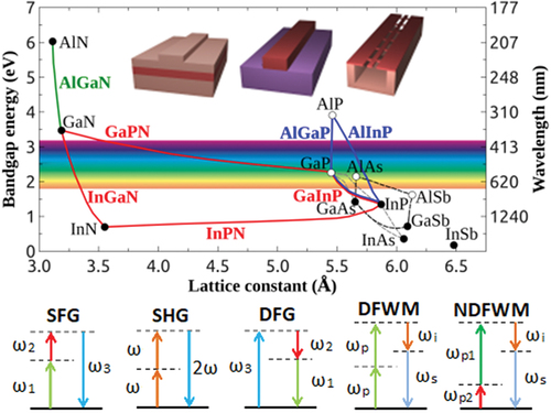
In , we present the bandgap energy as a function of the lattice constant for various III–V compounds. The wavelength equivalent of the bandgap energy is displayed on the right vertical axis. Binary compounds are represented in the graph by dots. The lines connecting two dots represent ternary compounds formed from the corresponding binary compounds. The areas subtended by the lines of the same color represent quaternary compounds formed from the four binaries (red for InGaPN, blue for AlGaInP, black for AlGaAsSb and grey for InGaAsP). The mutual concentrations of binaries in a ternary alloy provide a degree of freedom that can be varied to modify the alloy’s optical properties. The concentration dependence can be schematically represented as AxB1–xC where A, B, and C are single elements from the groups III and V of the periodic table, and is the content or fraction of the element A. In this regard, quaternary alloys have two degrees of freedom, and therefore provide more flexibility in achieving desired optical properties. They can be represented as A1–xBxCyD1–y.
Figure 1. Bandgap energy as a function of lattice constant for different III–V materials.
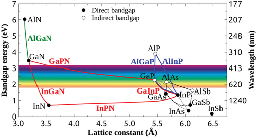
Vegard’s law provides a description of the desired bandgap energy, parameterized by the relative concentration of the III–V elements: , where
corresponds to the bandgap energy and A, B, and C are the III–V single elements [Citation95,Citation96]. Other material properties, like the refractive index, can also be calculated by this law. However, for some compositions or properties, a quadratic dependence on the concentration parameter
, known as the bowing parameter, is required [Citation95]. In a similar way, Vegard’s law for a quaternary compound takes the form
[Citation97].
Epitaxial growth of III–V semiconductors provides high-quality films having low defect density, which is crucial for quantum and nonlinear photonic applications [Citation98]. The ternary and quaternary alloys can be grown on binary substrates or on a previously grown epitaxial layer (epilayer). However, the lattice constant of the new layer must be matched to the previous one. Lattice mismatch leads to structural imperfections in the epilayers, which can act as recombination and scattering centers. The presence of such defects can result in significant scattering losses, hampering the integrated optical device’s performance.
If the two materials lie on the same vertical line on the graphic of , they can be grown lattice-matched. AlxGa1–xAs, for instance, can be grown lattice-matched on GaAs with all possible concentrations of aluminum. Substrates also play a crucial role in epitaxial growth. If the substrate is the same as the growth material, the growth is called homoepitaxy. Conversely, if the growth material is different from the substrate, the growth is referred to as heteroepitaxy [Citation99]. The presence of defects in heteroepitaxial growth from lattice and thermal mismatches presents a significant challenge. Therefore, buffer layers are often used to optimize the growth of high-quality heteroepitaxial thin films.
Various epitaxial growth techniques are utilized for III–V semiconductors, such as molecular beam epitaxy (MBE) [Citation100], metal-organic chemical vapor deposition (MOCVD) [Citation101], and liquid phase epitaxy (LPE) [Citation99]. MBE has a thickness precision at the angstrom level. A molecular beam is focused at a heated substrate and deposits atom-by-atom under controlled growth dynamics. It is capable of growing sharp interfaces and is widely used for electronic and optical devices. However, this growth technique is very costly and offers a slow growth rate, which limits its applicability and availability. MOCVD provides several advantages in this aspect. In particular, MOCVD provides a faster growth rate and lower cost. MOCVD is a chemical vapor deposition technique, which uses a flow of a gas-phase mixture containing precursors over a heated substrate for layer-by-layer deposition. This technique is capable of depositing a controlled thin layer with higher wafer throughput. It is widely used for integrated circuit applications. Finally, LPE is a low-cost deposition technique, which deposits material from a supersaturated solution. However, it is not capable of forming sharp junctions between two material layers. More recently, other cost-effective, large-area, and faster growth techniques have been explored for III–V semiconductors such as hybrid vapor phase epitaxy (HVPE) [Citation102], close-spaced vapor transport (CSVT) [Citation103], and thin-film vapor-liquid-solid (TF-VLS) growth [Citation104,Citation105]. The ongoing development of these techniques provides a pathway towards the commercialization of a cost-effective approach for III–V semiconductors for photonics.
Integrated optical devices like waveguides, photonic crystals, ring resonators, modulators, and interferometers mostly follow a standard top-down approach for fabrication, which includes the process of depositing a mask, writing the pattern on the mask, and transferring the pattern to the underlying material layers, as shown in . The fabrication can be followed by some post-processing if required. Before starting the top-down processes, the substrate with the epitaxial layers on it undergoes cleaning. This is done in several chemical cleaning steps, which usually apply acetone, isopropyl alcohol (IPA), and de-ionized water (DI water). Following this, drying is achieved by passing nitrogen over the surface or heating the material on a hot plate. Some of the important steps in a top-down fabrication process are detailed below.
Figure 2. A schematic diagram representing the top-down process of waveguide fabrication.
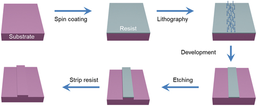
2.1. Resist deposition
The first step is to deposit a resist, made of polymer-solvent, via spin coating [Citation106]. The chemical properties of the resist change when exposed to light or electrons, depending on the resist type. In particular, there are two types of resists – positive and negative. The chemical bonds of the positive-tone resist loosen at places where they are exposed. As a result, exposed surfaces are dissolved in the developer solvent. Some common positive-tone resists are ZEP520a, PMMA, SPR 3000 series. On the other hand, negative-tone resists harden on exposure. In contrast to the previous case, areas that have not been hardened by the negative-tone resist dissolve in the developer solvent. Examples of negative-tone resists are HSQ, ma-N 1400 series and SU-8.
2.2. Lithography
The lithographic process can be performed with electrons in the case of electron-beam (ebeam) lithography, or with photons in the case of photo-lithography. In research settings, ebeam lithography is most frequently used for writing patterns with sub-micrometer features. With ebeam lithography, a beam of electrons hits the material surface coated with the resist and changes its chemical properties. After passing the electron beam, exposed areas dissolve (or harden) when immersed in the developer solvent. Although ebeam lithography is a slow process, it can produce feature sizes with critical dimensions in the range of 3–5 nm. Photo-lithography exposes the resist to ultraviolet light with typical wavelengths of 100 to 400 nm (UV lithography) [Citation107]. Photo-lithography has seen substantial improvements over the past five years, in particular with extreme ultraviolet (EUV) lithography systems being commercially produced by semiconductor manufacturers like ASML and Intel [Citation108]. With EUV systems, resolution limits can reach sub-20-nm structures using radiation sources with a wavelength of 13.5 nm. However, the throughput achievable with EUV systems is still not comparable to the earlier generations of photo-lithography systems because of limitations such as source brightness and low industry-grade EUV resist availability [Citation109].
2.3. Etching
Once the pattern is created in the resist, the process of transferring the pattern to the underlying material, known as etching, is performed. Etching can be done using wet chemicals (wet etching) which results in very isotropic and smooth structures, as well as using plasma etching (dry etching), in which there are more variables to tune and therefore the outcome results in more controlled and anisotropic features. ICP-RIE (Inductively Coupled Plasma Reactive Ion Etching) is the most commonly used system for plasma etching. This method allows for the control of parameters like ICP power, bias power, chamber pressure and temperature, gas flows, etc., which results in increased control over material removal. III–V alloys are often etched in chlorine-based plasma [Citation110], using gases such as Cl2, BCl3, CCl4, SiCl4.
In some systems, inert gases like argon and helium are also added to increase the etch rate and to achieve a more anisotropic etch result. These gases do not react or combine with the substrate to create new radicals, but contribute more to the physical etching by bombarding the substrate with the heavier non-reacting atoms/ions, which ablate the radicals produced by the other gases. The result is an increased etch rate with well-defined vertical sidewalls.
For some III–V device structures which require deeper etch depths, standard resists are insufficient if they are ablated too quickly [Citation111,Citation112]. In these cases, a mask that erodes more slowly is required. Such masks are known as hard masks and provide a much slower etch rate. In addition, they enable a large selection of materials suitable for etching. Thermally deposited oxide (or silica) is known to be a great hard mask with a very low etch rate in chlorine-based chemicals and provides selectivity of around 1:10 for most of the III–V alloys. Selectivity is defined as the ratio of the amount of mask etched to the amount of material etched. In other words, up to 10 nm of III–V material can be etched for each 1 nm of silica mask.
Some integrated photonic devices based on III–V semiconductors require additional steps to ensure proper function. These additional stages are known as post-processing steps. These usually involve treating the components with chemicals to improve device quality; for instance, by creating smoother sidewalls or treating the devices with acids to remove or dissolve some sacrificial layers [Citation113,Citation114].
III–V semiconductors are suitable for the implementation of active (electrically controlled) photonic devices. However, there is an ongoing effort to produce photonic structures compatible with existing capabilities of the microelectronics industry. In addition, optical waveguides in III–V materials often lack in performance when compared to low-loss silicon waveguides. As a result, there has been growing interest in heterogeneous integration to use active III–V components with passive silicon photonic components. Consequently, wafer-bonding is frequently used to attach III–V active structures on silicon platforms. When two smooth surfaces of any material are brought together in close proximity, a combination of Van der Waals forces and other additional inputs like temperature and pressure, it allows for the two materials to form bonds in a process referred to as wafer-bonding [Citation115]. Recently, the wafer-bonding process has been deployed to create novel AlGaAs-on-insulator (AlGaAs-OI) platforms, which continue to find new applications in nonlinear optics [Citation116,Citation117].
In this section, we focused on the fabrication processes for nonlinear photonic devices. However, there are still several other processes, beyond the scope of this review, that are needed to fabricate the electrical pads and circuitry required for electrical signal processing [Citation118,Citation119]. These electrical connections are required for the operation of modulators, interferometers, detectors, heaters, lasers, and other active components. In addition, photonic chips ready for commercialization and perhaps integration in more complex optoelectronic systems, such as the ones described in section 5, typically require further packaging [Citation120–122].
3. Nonlinear optical processes and coefficients
Light-matter interactions can be classically modeled as oscillating electric dipoles (from the electron/proton separation of the material’s atoms) driven by the oscillating electric field of the light wave. The polarization vector can be expressed, in general, in terms of a series of tensor products between the light’s electric field vector
and the material’s
-th order optical susceptibilities,
[Citation123], as
In EquationEquation (1)(1)
(1) , the
are
-rank tensors. For instance,
is a second-rank tensor (
matrix) related to the linear optical properties of the medium, including anisotropic and birefringent materials. Similarly, the second-order optical susceptibility,
, is related to the second-order nonlinear optical phenomena, and the third-order susceptibility,
, to the third-order phenomena, and so on [Citation123].
To discuss the nonlinear photonics of each III–V material platform, we introduce some second-order and third-order nonlinear optical phenomena, and define their main nonlinear coefficients.
3.1. Second-order processes
To investigate the second-order processes, let us assume the electric field as , where
are the electric field amplitudes. Therefore, the second term in EquationEquation (1)
(1)
(1) can be expressed as
Four different second-order nonlinear optical phenomena are expressed as the different terms in EquationEquation (2)(2)
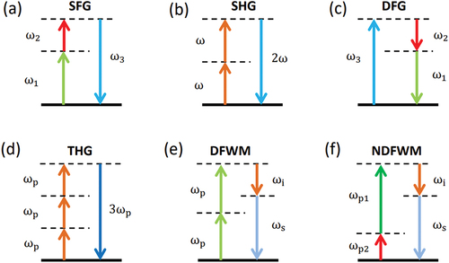
(2) . The first and second terms demonstrate second-harmonic generation (SHG). The third and fourth terms indicate sum-frequency generation (SFG) and difference frequency generation (DFG), respectively. The last term denotes optical rectification (OR) [Citation123].
In terms of energy conservation of the photons’ interactions, SFG, SHG, and DFG can be illustrated as ). Each of these processes can be used for some application. For instance, many wavelength conversion systems utilize these nonlinear optical processes. New coherent light components can be generated either at shorter (SHG, SFG) or longer (DFG) wavelengths than those of the incident beams. Yet, they also are the foundation for experimental techniques used to measure the nonlinear optical property of the sample. For instance, the power of the transmitted or reflected light component generated by SHG, SFG or DFG can be compared to the power(s) of the incident beam(s) to experimentally determine the value of . Often, the experiment measures the nonlinear susceptibility tensor elements
, related to the susceptibility by
[Citation123]. In some cases, depending on the experimental conditions, the technique is only able to measure the average effect of the tensor elements as an effective nonlinear optical property, i.e. effective
or effective
.
Figure 3. Illustration of energy levels for second- and third-order nonlinear optical phenomena: (a) sum frequency generation, (b) second-harmonic generation, (c) difference frequency generation, (d) third-harmonic generation, (e) degenerate four-wave mixing, (f) nondegenerate four-wave mixing. The dashed lines show virtual states.
3.2. Third-order processes
Considering the third term in EquationEquation (1)(1)
(1) and assuming the electric field as
, the third-order polarization
can be calculated, resulting in 44 different frequency terms. Among them, the terms with frequencies
,
and
describe the process called third-harmonic generation (THG), in which three photons with the same frequency are annihilated, creating a photon of tripled frequency (). On the other hand, some of the terms with two or three interacting frequencies can lead to another third-order phenomenon known as four-wave mixing (FWM), in which two photons with the same (degenerate case) or different frequencies (nondegenerate case) are annihilated, creating two photons with different frequencies ()). Other commonly encountered third-order processes are self-phase modulation (SPM) and cross-phase modulation (XPM). In SPM, a propagating intense pulse causes a change in the refractive index of the medium as a consequence of the optical Kerr effect (discussed below). As a result, the pulse obtains a varying phase in terms of intensity and the spectrum is consequently modified, producing spectral broadening or spectral narrowing. XPM is similar to SPM, but involves more than one light beam; the most intense beam changes the refractive index of the medium, affecting the phase and spectral features of the other beam(s).
One of the most important third-order nonlinear optical properties of a photonic material is the nonlinear refractive index (). The nonlinear refractive index characterizes the optical Kerr effect, i.e. the effect in which the refractive index,
, depends on the intensity,
, of the illuminating light according to
where is the linear refractive index (refractive index for the low-intensity light regime). The intensity
is proportional to the square of the electric field amplitude [Citation124].
As the nonlinear component of the refractive index is proportional to the optical intensity, a beam with a non-uniform transverse spatial profile (e.g. a Gaussian beam) experiences a non-uniform refractive index. As a consequence, the medium behaves like a lens (optical Kerr lens). Positive causes self-focusing, while a negative
causes self-defocusing [Citation123]. These effects are exploited in the closed-aperture Z-Scan technique [Citation125–127] to measure
of bulk or thin-film materials. In Z-Scan, the sample is moved along a focused Gaussian beam while the transmittance is measured at the far field to quantify the self-(de)focusing strength [Citation125]. However, ZS requires a thin-sample approximation that does not hold for waveguides. Therefore, it is common to measure
of photonic devices by techniques based mainly on SPM and FWM (see examples in ). The sign of
is positive in semiconductor materials for the photon energies significantly smaller compared to the bandgap energy. This represents the case of self-focusing. However, for the photon energies close to the band edge,
becomes large and negative [Citation87,Citation90,Citation91,Citation93], which naturally allows one to avoid the catastrophic self-focusing in that highly nonlinear regime.
Table 1. Experimental values of the nonlinear coefficients measured in bulk GaAs/AlGaAs materials and waveguides.
Table 2. Nonlinear optical properties of III-nitride semiconductors.
Table 3. Nonlinear optical properties of InP/InGaAsP waveguides.
Photonic waveguides, in particular, bring the possibility of tightly confined light in a small propagation mode area, which results in a high intensity of propagating light. The nonlinear coefficient, , includes the nonlinear refractive index
and the confinement strength (mode area) through the relation [Citation128]
where is the wavelength of light in free space. The
parameter is often used as a quantitative characteristic that provides insight into the nonlinear interaction strength arising from the combination of the nonlinear index and light confinement.
The effective mode area for a third-order nonlinear process, , is calculated by the expression
The integration in EquationEquation (5)(5)
(5) is performed over the entire cross-sectional
-
plane, and
represents the electric field inside the waveguide. This equation is often used in a software for finite-difference eigenmode (FDE) calculations, like the Lumerical Mode Solutions, as a practical way to design and simulate photonic devices. However, it assumes some approximations, such as a constant refractive index. For a more general set of equations for
and
, including effects of different refractive index in multi-layer waveguides, we refer the reader to Refs. [Citation129,Citation130].
Another key parameter in the characterization of a nonlinear photonic device is the 2PA coefficient (), related to the 2PA effect (electronic transitions caused by the simultaneous absorption of two-photons). The intensity-dependent nonlinear absorption coefficient (
), when 2PA is present, is given by:
The term in EquationEquation (6)
(6)
(6) represents linear absorption in a bulk material when illuminated at a wavelength in its transparency window. In addition to linear absorption,
for waveguides includes the effects of mode leakage and light scattering. For this reason, it is often called the propagation loss coefficient. Two-photon absorption usually hampers photonic device performance by increasing optical power loss in the high-intensity nonlinear regime. However, 2PA might be useful in some applications, such as optical switching and optical limiting. For instance, some optical switches use free-carriers generated by 2PA to produce the refractive index changes required for their operation [Citation131]. In the case of optical limiting, 2PA helps protects downstream devices from damages due to high optical power [Citation132].
The 2PA coefficient is often measured by the nonlinear transmittance technique (NLT), where the output intensity, subjected to nonlinear absorption, is expressed as a function of the input intensity [Citation31]. In bulk materials and thin-films, the open-aperture ZS technique is also a good option for measurements [Citation127]. In addition, the data analysis of other third-order nonlinear optical experiments may also include the effect of 2PA. Thus,
can be also measured by FWM and SPM, for example (see references in ).
The nonlinear parameters and
are analytically related to the third-order susceptibility by
and
, respectively [Citation124]. As in the case of second-order coefficients, the measured values of
,
, and
in waveguide structures are often different from the bulk-material values. They are therefore referred to as effective nonlinear coefficients. Additionally, the properties can depend on the light polarization in anisotropic materials. This can be exploited to determine different elements of the
tensor [Citation133,Citation134].
There is at least five orders of magnitude variation between the values of various semiconductor materials (e.g. ZnSe and InSb). This is greater than the difference in the values of
in silica and GaAs (
of GaAs is 500 larger). However, this fits within the prediction of the overall
scaling with the bandgap energy as
[Citation93].
3.3. Higher-order processes
Experiments on fourth-, fifth-, and higher-order nonlinear optical processes are rare since the lower-order processes typically dominate in nonlinear interactions. An exception is the three-photon absorption (3PA), a fifth-order nonlinear optical process in which three photons are simultaneously absorbed in an electronic transition. The intensity-dependent absorption coefficient, subjected to 3PA, is given by [Citation124], where
is the 3PA coefficient. Photonic devices operating in a spectral region without 2PA might still exhibit nonlinear losses associated with 3PA [Citation31].
4. Main material platforms
In this section, we introduce the common III–V semiconductor platforms that have been explored for nonlinear photonics applications, present the nonlinear coefficients measured for their representative materials, and give an overview of the devices realized in these platforms. A few nonlinear optical measurements have also been performed in bulk and thin-films of III–V semiconductors, such as InSb and InN [Citation135–137]. However, they are not covered in this review because their technology is not yet mature enough to turn them into platforms for fabrication of nonlinear photonic devices.
4.1. GaAs/AlGaAs
Gallium arsenide (GaAs) is a binary semiconductor with a bandgap close to (
) [Citation138]. In addition to its applications in electronics and opto-electronics, GaAs is a very well-explored III–V material for photonics. It presents a wide transparency window, from
to
, a high refractive index (
at
[Citation138]) similar to silicon, and high values of
,
, and
(see ).
GaAs and AlAs have fairly close lattice constants of and
, respectively [Citation95]. Therefore, AlxGa1–xAs with
can be epitaxially grown on GaAs substrate with a negligible lattice mismatch.
Many different photonic devices have been demonstrated in (Al)GaAs, for example: low-loss, high-confinement waveguides, micro-ring resonators with high Q-factors, photonic crystal waveguides and cavities for SHG, correlated-photon sources using spontaneous parametric down-conversion (SPDC), superconducting detectors, low-power modulators for fast control and manipulation of photons, and directional couplers for single-photon and two-photon state manipulation [Citation139–143]. represents some waveguide geometries based on AlGaAs platforms that have been used for nonlinear optical processes.
Figure 4. Illustration of different AlGaAs waveguide geometries used in nonlinear photonics: (a) AlGaAs heterostructures, (b) AlGaAs-OI, (c) AlGaAs air-bridge waveguides. The darker layers in (a) and (b) represent the guiding layers.
AlGaAs heterostructures [see )] have been implemented since early 1990s [Citation12,Citation13,Citation15,Citation17,Citation19,Citation21–24,Citation29,Citation31] for nonlinear experiments. They represent the simplest waveguide structures typically requiring a single-step epitaxy and lithography. The guiding layer (or core) has lower aluminum concentration relative to the surrounded claddings. Consequently, the refractive index contrast is produced, sufficient for light confinement in the core. Optical waveguides produced in such a manner, typically referred to as strip-loaded waveguides, are robust against fabrication errors due to a shallow etching [Citation111,Citation144]. Such devices, however, exhibit moderate nonlinear optical interactions due to their lower compactness and moderate refractive index contrasts. To achieve a higher compactness, deeply-etched waveguide structures, termed AlGaAs nanowires, have been implemented in the 2000th [Citation111,Citation144–148]. Such structures enable superior compactness, dispersion engineering and permit modal-phase-matched (MPM) second-order nonlinear interactions [Citation146].
AlGaAs-on-insulator (AlGaAs-OI) waveguide platform [Citation116,Citation140,Citation149–157], where, using some wet chemical etching and wafer bonding, a thin layer or AlGaAs with epitaxially grown silica as substrate can be bonded onto a template wafer [see )], has started gaining attention in 2010. AlGaAs-OI devices can have extremely small modal areas and, according to EquationEquation (4)(4)
(4) , high values of
. As such, they represent efficient nonlinear photonic devices: both
[Citation140,Citation153,Citation156] and
[Citation116,Citation149–151,Citation154,Citation155,Citation157] nonlinear interactions have been readily demonstrated in these waveguides.
Further, the cladding material of AlGaAs structures can be removed on both the sides using wet chemical etching methods to create air claddings [see )]. Such structures are known as air-bridged, or suspended, waveguides [Citation158–160]. Suspended structures have the advantage of enabling large index contrasts, which is important for optical confinement. Thanks to their high cross-sectional asymmetry, MPM second-order nonlinear optical interactions are readily achievable [Citation159,Citation160] in these structures.
In terms of the nonlinear optical performance, AlGaAs-OI has presented the record-high nonlinear coefficient among all the AlGaAs platforms: [Citation154]. Record-high SHG conversion efficiencies of
%/(W cm2) in suspended AlGaAs [Citation158],
%/(W cm2) in GaAs-OI [Citation161] and FWM conversion efficiency of
in AlGaAs-OI waveguides [Citation149] were demonstrated. The achieved FWM conversion bandwidth of 750 nm is also remarkable when compared with other photonic platforms [Citation149].
In , we summarize the values of the nonlinear coefficients experimentally obtained in bulk GaAs and in (Al)GaAs waveguides of different kinds. For the table entries, we gave preferences to the publications where wavelength dependencies of the nonlinear parameters were presented. A more extensive and detailed list of nonlinear coefficients, conversion efficiencies, and a more in-depth review of (Al)GaAs waveguide platforms will be provided in the upcoming review article [Citation162].
4.2. III-nitrides
Group III-nitrides is a popular platform for power electronics, analogue circuits, and optoelectronic applications owing to their wurtzite crystal structure, direct bandgap, high electron mobility, and chemical and thermal stability [Citation100,Citation170,Citation171].
The bandgap of III-nitrides can be tuned from to
by varying the metal composition between Al, Ga, and In to synthesise aluminium nitride (AlN), gallium nitride (GaN), and indium nitride (InN), respectively [Citation170]. Foreign substrates, i.e. sapphire, silicon, and silicon carbide (SiC), are used to grow epitaxial GaN films because of the unavailability of the native substrates [Citation174]. There is a large lattice and thermal mismatch between GaN and the foreign substrates that leads to high dislocation density in GaN. These defects act as recombination centers, thereby leading to additional optical losses. The epitaxial quality of GaN film can be improved by incorporating buffer layers between the GaN and the substrates, which helps in offsetting the mismatch effects [Citation114,Citation175,Citation176].
Group III-nitrides, specially GaN and AlN, owing to their optical properties and wide transmission ranges, are strong candidates for nonlinear optical applications [Citation177]. GaN has a combined transparency range of LiNbO3 and GaAs ( to
), and therefore this material has a potential of generating wavelengths in either far-IR or near-UV by SFG or DFG [Citation178]. Additionally, GaN exhibits both
and
nonlinearities, and a higher nonlinear refractive index, which is advantageous for the applications in all-optical signal processing at the Telecom wavelengths. Furthermore, the large bandgaps of GaN and AlN ensure the absence of the 2PA and 3PA at the telecommunications wavelengths.
A schematic of nonlinear waveguides based on III-nitrides is shown in . Among these are GaN on AlGaN [Citation172], GaN on AlN [Citation171], GaN-on-sapphire [Citation173] and on gallium oxide [Citation114]. Additionally, air-suspended GaN waveguides and photonic crystal membranes have been successfully fabricated [Citation179] [see )]. Furthermore, a success in the propagation loss reduction in GaN waveguides has been recently achieved. GaN waveguides with the propagation loss coefficients as low as at
,
at
, and
at
have been realized [Citation180–182].
Figure 5. Schematics of III-nitride waveguide structures. (a) and (b) GaN/AlN [Citation171], (c) GaN/AlGaN [Citation172], (d) GaN-on-Sapphire [Citation173], (e) GaN on Ga2O3 [Citation114].
![Figure 5. Schematics of III-nitride waveguide structures. (a) and (b) GaN/AlN [Citation171], (c) GaN/AlGaN [Citation172], (d) GaN-on-Sapphire [Citation173], (e) GaN on Ga2O3 [Citation114].](/cms/asset/43955c53-9614-4680-bae2-03a51ef35187/tapx_a_2097020_f0005_oc.jpg)
Figure 6. Scanning electron microscopy (SEM) images of (a) a GaN wire waveguides suspended with tethers. Reprinted with permission from [Citation179] © The Optical Society; and (b) AlN-based microring resonators before their encapsulation. Reproduced from [Citation183] with the permission of AIP Publishing.
![Figure 6. Scanning electron microscopy (SEM) images of (a) a GaN wire waveguides suspended with tethers. Reprinted with permission from [Citation179] © The Optical Society; and (b) AlN-based microring resonators before their encapsulation. Reproduced from [Citation183] with the permission of AIP Publishing.](/cms/asset/0a8b161b-9cb4-4798-953e-7d16535cf17a/tapx_a_2097020_f0006_oc.jpg)
Higher-order terms in nonlinear polarization come into play at higher light intensities. Therefore, in integrated photonic devices, where the input power ranges from microwatt to milliwatt, it is crucial to employ resonant structures such as ring resonators with high quality (Q)-factors to observe higher-order nonlinear effects. High-Q-factor microring resonators (MRR) based on GaN have been demonstrated in [Citation173,Citation184]. A quality factor exceeding in the near-infrared, infrared, and visible wavelength ranges [Citation184], and a quality factor of
at the Telecom wavelength range [Citation173] have been reported. Micromechanical coupled ring resonators have also been fabricated using AlGaN/GaN heterostructures, demonstrating a Q-factor of 8350 at
[Citation185]. Additionally, AlN-based ring resonators have demonstrated high Q-factors of
with propagation losses as low as
at
[Citation186]. Furthermore, a quality factor of 5400 was reported in a photonic crystal waveguide using GaN nanowires, operating at
[Citation179]. A successful demonstration of high-Q-factor microcavities based on single-crystal AlN has been performed in [Citation183] [see also ) for an SEM image]. An exemplary SHG conversion efficiency of 17,000%/W has been achieved in these devices [Citation183].
Due to the challenges associated with defect mitigation and lack of native substrate, nonlinear integrated photonics based on III-nitrides is still at an early stage of development. There are only a few studies reporting the measurement of the second- and third-order nonlinear optical coefficients in AlN and GaN waveguides. We present these results, together with some nonlinear coefficient measurements in bulk materials, in .
4.3. InP/InGaAsP
InP is an increasingly important platform for photonic integrated circuits since it allows for the monolithic integration of several active components, such as lasers, semiconductor optical amplifiers, photodetectors, modulators with passive devices [Citation191]. Furthermore, InP-based membranes have been fabricated with high index contrasts, resulting in micron-scale devices with a full set of photonic functions [Citation192].
InGaAsP shows strong potential as a material platform for nonlinear photonic devices [Citation193]. A major limiting factor, however, is the low optical confinement in the ridge waveguide structures on the InP substrate. The low confinement factor results in waveguide dimensions of several micrometers, and minimum bending radii of tens to hundreds of micrometers [Citation194]. Nevertheless, the optical confinement in the waveguides can be tuned by implementing a low-index optical buffer layer between the waveguide and the substrate carrier [Citation195]. Due to its bandgap energy of , InGaAsP is subject to 2PA at the Telecom C-band wavelengths [Citation114]. The 2PA coefficient of InGaAsP multi-quantum-well waveguides has been reported to be
at
[Citation44], which is much larger than that of AlGaAs () and silicon. However, InGaAsP is a well-established material platform for semiconductor lasers. Therefore, combining low-loss optical waveguides with InGaAsP multi-quantum-well lasers on the same chip is a critical research direction for extending the operating range of the lasers to longer wavelengths.
For active InGaAsP/InP integration, free-carrier absorption is typically the main contributor to the propagation loss [Citation196]. This can be tackled by using additional butt-joint or complicated selective area re-growth schemes [Citation197], however, this method significantly complicates the fabrication process because of strict control requirements of etching and epitaxial regrowth.
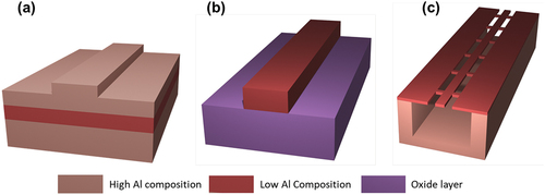
presents some waveguide structures realized in InGaAsP/InP platform. In particular, ) presents an SEM image from the facet of an InGaAsP strip-loaded (partly etched through the upper cladding) waveguide. ) shows a schematics of the cross-sectional geometry and material composition of a typical InGaAsP waveguide [Citation193]. ) illustrates an InP-based hybrid plasmonic waveguide [Citation198].
Figure 7. Some possible structures for InGaAsP waveguides. (a) Scanning electron microscope image of the facet of a strip-loaded InGaAsP waveguide Reprinted with permission from [Citation193]. (b) and (c) show the schematics of an InGaAsP strip-loaded [Citation193] and an InP-based hybrid-plasmonic waveguide [Citation198], respectively.
![Figure 7. Some possible structures for InGaAsP waveguides. (a) Scanning electron microscope image of the facet of a strip-loaded InGaAsP waveguide Reprinted with permission from [Citation193]. (b) and (c) show the schematics of an InGaAsP strip-loaded [Citation193] and an InP-based hybrid-plasmonic waveguide [Citation198], respectively.](/cms/asset/2768bd0b-f537-4047-8440-4db647e324ca/tapx_a_2097020_f0007_oc.jpg)
InxGa1–xAsyP1–y/InP strip-loaded waveguides have been experimentally studied by SPM, FWM, and NLT techniques [Citation193]. The nonlinear coefficient, measured by SPM, has a moredate value of . The FWM conversion range, defined as the wavelength difference between maximally separated signal and idler spectral components, is measured as
. The 2PA coefficient was also determined for this waveguide by NLT as
at
. Finally, FWM was performed in an InGaAsP/InP single-quantum-well waveguide to measure
and
from
to
. The maximum values in the range were
,
, and
at
[Citation48].
The FWM conversion efficiency was measured as and around
when the waveguides were pumped at
by a picosecond-pulsed laser and continuous-wave (CW) laser, respectively [Citation47,Citation48,Citation199]. The higher generation of free-carriers in the CW case was attributed as the cause for the lower efficiency. Indeed, after exposing the waveguide to a proton bombardment dose of
to decrease the free-carrier lifetime, the CW FWM efficiency increased by
[Citation199]. Furthermore, simulation results indicate that the nonlinear coefficient of an InP-based hybrid plasmonic waveguide (HPW), as shown in ), might reach a value of
at
[Citation198], which is comparable with an SOI-based HPW [Citation200]. summarizes a selection of some InP/InGaAsP nonlinear photonic devices and reports their nonlinear parameters.
4.4. GaP
GaP is an indirect bandgap semiconductor with a bandgap of and a large transparency range spanning from the visible to mid-IR (
to
), which has been traditionally used to make green light emitting diodes. GaP has a wurtzite crystal structure and a large linear refractive index value of around
in the C- and L-bands. Some measured nonlinear optical parameters are:
and
at
[Citation201,Citation202]. Z-scan measurements were performed in orientation-patterned GaP resulting in
at
and
at
[Citation203]. Nanophotonic devices based on GaP platform attract significant attention because GaP can be grown on silicon with minimal lattice mismatch, thereby allowing for heterogenous integration. For strong optical confinement in nanophotonic devices, a larger index contrast between the core and cladding is desired. Recently, it was demonstrated that GaP on silica can be fabricated through a wafer-bonding process [Citation204]. Devices, such as waveguides with propagation loss coefficients as low as
, ring resonators with quality factors of
, grating couplers with insertion losses as low as
, and nonlinear frequency conversion processes such as SHG and THG have been demonstrated in this platform [Citation204]. Recently, in [Citation205], the authors demonstrated that GaP can be grown directly on sapphire using MBE, which is possible by domain-matching epitaxy. Additionally, metasurfaces supporting high-Q-factor quasi-BIC (bound states in the continuum) have been demonstrated. There have also been efforts made for high-speed all-optical switching with the experimental switching times under
[Citation206].
4.5. InGaP
InGaP is a ternary alloy commonly used in multi-junction solar cells [Citation207,Citation208], but it has also gained attention for its large linear refractive index of around at
, and large second-order nonlinearity (
, comparable to that of GaAs. Its bandgap energy of
(
) inhibits 2PA in the telecommunications wavelength range. InGaP can be grown on GaAs with negligible lattice mismatch but the index difference between these two materials does not provide enough contrast useful for integrated photonic applications. Therefore, InGaP on silica is used as a common platform, fabricated using the processes of systematic wet etching of some epilayers and wafer bonding.
Waveguides with a propagation loss coefficient of , high nonlinear coefficient
, and 3PA coefficient
have been fabricated and used in FWM and NLT experiments conducted in the Telecom C-band [Citation209]. Its high Kerr nonlinearity was employed to demonstrate
-octave-spanning supercontinuum generation [Citation210]. Photonic crystal cavity-based optical parametric oscillator has been demonstrated [Citation211]. Most recently, SHG in high-Q-factor ring resonators (
) and photon-pair generation via spontaneous parametric down-conversion (SPDC) with a rate of
have also been reported [Citation212].
5. Current and future applications
Mirroring the development of novel applications in more accessible silicon photonics (SiP) platform during the late 2000s and early 2010s, the number of developments in III–V materials has exploded since the end of the recent decade. Owing to their bandgap and lattice constants, much of the research in III–V materials has been driven by a desire to monolithically integrate optical functionalities and controlling electronics together with optical sources and detectors – something difficult to accomplish in SiP. In this section, we present key recent developments and possible future directions for III–V material applications in three categories: (1) telecommunications, (2) computation and information science, and (3) sensing and imaging.
5.1. Telecommunications
Group III–V materials have a long history of use in the telecommunications industry. For instance, InGaAs/GaAs and InGaAsP/InP operating at telecom wavelengths have been extensively studied and commercialized over the past 30 years [Citation213,Citation214]. In addition, quantum-well lasers on GaAs/AlGaAsP platforms have been used for numerous room-temperature applications [Citation215,Citation216]. Even today, InP-based integration platforms are widely used by major telecommunications hardware manufacturers for high-performance transceivers [Citation118], and major industry acquisitions have been driven by desires to excel in InP photonics [Citation217,Citation218].
The implementation of optical frequency combs (OFCs) through Kerr nonlinearities, either FWM or SPM, is an important functionality for optical communication systems. OFCs have been used in a multitude of applications, including precision timing and synchronization, distance measurements, and frequency conversion. Due to their highly nonlinear properties, III–V materials are frequently chosen platforms for OFC generation. For instance, efficient OFC generation devices have been demonstrated in integrated GaP [Citation202], GaN [Citation175], AlN [Citation219], InP/InGaAsP [Citation220,Citation221], and AlGaAs-on-insulator [Citation116,Citation222]. Due to its technical simplicity, another method of generating OFCs is via quantum-dash mode-locked laser diodes (QD-MLLD). Recent demonstrations of QD-MLLDs in InP/InGaAsP platforms have shown promise in the design of compact integrated multi-wavelength sources and local oscillators [Citation223] (see ). Most recently, the operational simplicity of QD-MLLDs has been utilized in the demonstration of a reconfigurable microwave photonic filter [Citation224], opening a wide range of possible applications in radio-frequency signal processing and radio-over-fiber communications.
Figure 8. (a) Cross-section of an InAs/InP quantum-dash mode-locked laser diode (QD-MLLD) used in a reconfigurable microwave photonic filter. (b) Fully-packaged QD-MLLD. (c) Optical spectrum with 300 mA injection current. Reprinted with permission from [Citation224] © The Optical Society.
![Figure 8. (a) Cross-section of an InAs/InP quantum-dash mode-locked laser diode (QD-MLLD) used in a reconfigurable microwave photonic filter. (b) Fully-packaged QD-MLLD. (c) Optical spectrum with 300 mA injection current. Reprinted with permission from [Citation224] © The Optical Society.](/cms/asset/39d7c7c1-d2fd-4d61-9165-6189405b0f3b/tapx_a_2097020_f0008_oc.jpg)
In addition to OFC generation, III–V platforms are also well-suited for wavelength conversion through various harmonic generation processes. Several of these spectral conversion devices have been demonstrated in AlN [Citation183,Citation225], GaAs [Citation152,Citation153], GaP [Citation226], and AlGaAs [Citation227] at very high efficiency (see ). Co-integration with electronic components will likely lead to further usage of III–V SHG and THG sources in quantum photonics. In addition, classical coherent communications will see benefits from smaller device footprints and lower pump power requirements [Citation152].
Figure 9. Adapted from [Citation226]. (a) Scanning electron microscope image of a GaP microdisk (prior to undercutting) used for wavelength conversion via nonlinear processes. (b) Illustration of nonlinear polarization generated by TE mode in a GaP microdisk at 1550 nm. Reproduced from [Citation226] with the permission of AIP Publishing.
![Figure 9. Adapted from [Citation226]. (a) Scanning electron microscope image of a GaP microdisk (prior to undercutting) used for wavelength conversion via nonlinear processes. (b) Illustration of nonlinear polarization generated by TE mode in a GaP microdisk at 1550 nm. Reproduced from [Citation226] with the permission of AIP Publishing.](/cms/asset/4428760f-011d-455f-b5a4-772e3f010398/tapx_a_2097020_f0009_oc.jpg)
While much of the discussion thus far has focused on guided optical communications, III–V materials are also finding niche free-space applications. One example uses GaAs/AlGaAs to implement a travelling-wave modulator for V-band space applications [Citation228]. GaAs is notable for its temperature stability and high radiation damage threshold and has historically been the III–V material of choice for many satellites’ solar cells, such as the ones used on the Venera 2 and Venera 3 missions to Venus [Citation229]. Looking forward, GaAs will likely remain a key material platform for integrated photonics in harsh extraterrestrial environments.
5.2. Computation and information science
The field of quantum information science has long looked to the fields of optics and photonics to implement quantum communications protocols. Several quantum key distribution (QKD) protocols have been successfully demonstrated in partially integrated SiP [Citation230,Citation231]. A significant concern with SiP is that sources, gain media, and detectors are difficult to integrate. Current SiP QKD systems rely on off-chip detectors and sources [Citation230,Citation232], which imposes significant operational costs in terms of power consumption and data center floor space. To compete with existing commercial transceivers, future metropolitan-scale QKD systems will need to be miniaturized via integration. A likely resolution to this problem involves monolithic system integration in a III–V material platform, where all necessary active and passive components are readily available.
Moreover, integrated InGaAsP/InP single-photon detectors have been demonstrated with minimal cooling requirements [Citation233] at telecommunications wavelengths, while photon pair generation has been observed via nonlinear processes in AlGaAs [Citation157,Citation234,Citation235]. To complement these functionalities, InP quantum random number generators [Citation236] (see ) and integrated Fredkin gates [Citation237] could lead to a powerful suite of components to implement quantum algorithms on a chip. As a result, III–V platforms will likely be important materials for the future of quantum information science.
Figure 10. An integrated quantum random number generator in InP. (a) Operational schematic of QRNG based on two-laser interference. (b) Principle of operation: a pulsed laser interferes with a continuous laser to create a measurable random phase, which is subsequently digitized into a random value. (c) Image of a single chip with two integrated QRNG devices on a 1 Euro cent. Reprinted with permission from [Citation236] © The Optical Society.
![Figure 10. An integrated quantum random number generator in InP. (a) Operational schematic of QRNG based on two-laser interference. (b) Principle of operation: a pulsed laser interferes with a continuous laser to create a measurable random phase, which is subsequently digitized into a random value. (c) Image of a single chip with two integrated QRNG devices on a 1 Euro cent. Reprinted with permission from [Citation236] © The Optical Society.](/cms/asset/e1388b2e-979c-48ea-8516-6335622d49e6/tapx_a_2097020_f0010_oc.jpg)
5.3. Sensing and imaging
Photonic biosensors are a promising alternative to costly laboratory procedures, such as enzyme-linked immunosorbent assays. In particular, the ability of photonic biosensors to perform label-free detection makes them subjects of interest for lab-on-chip devices. While much work has been done in this field with SiP platforms, the difficulty of integrating light sources and detectors again creates an opportunity for III–V materials to excel where SiP cannot. Biophotonic functions have been demonstrated in III–Vs, such as GaAs/AlGaAs [Citation238] and InP [Citation239] (see ) for label-free pathogen detection. The co-integration of broadband frequency comb generators, sensing devices, and detectors may soon lead to rapid, cost-effective home-diagnosis biophotonic chips. In addition to attractive biosensing functionalities, III–V materials are well suited for imaging. A recent biophotonic example uses InP quantum dots to demonstrate tunable, near-infrared photoluminescence and multiplexed in vivo imaging [Citation240].
Figure 11. A schematic representation of an electronic InP biosensor for label-free detection. The device’s active area is functionalized via amination, PEGylation, and covalent coupling of biomolecular receptors to detect the presence of specific ligands. Reprinted with permission from [Citation239].
![Figure 11. A schematic representation of an electronic InP biosensor for label-free detection. The device’s active area is functionalized via amination, PEGylation, and covalent coupling of biomolecular receptors to detect the presence of specific ligands. Reprinted with permission from [Citation239].](/cms/asset/5cde0d16-e0fb-47ae-8d07-b28c6e30e95d/tapx_a_2097020_f0011_oc.jpg)
A topic of note is the use of frequency combs in astrophysics. Astro-combs have been used in several areas of astrophysics, such as measurements of Doppler shifts and high-precision astronomical spectroscopy [Citation241]. Astro-combs are a relatively recent development and have not yet been implemented in III–V materials. One interesting research direction would be to use the high temperature stability of GaAs/AlGaAs systems for space-based satellite imaging and spectroscopy.
6. Conclusions
In summary, we have reviewed a range of important works demonstrating nonlinear optical processes achieved with integrated III–V material platforms. In addition, this work provides a theoretical introduction to nonlinear optical processes, as well as descriptions of some fabrication processes to realize these structures. Although some of these platforms like GaAs/AlGaAs, and InP have been extensively studied for nonlinear optical processes, there still remains much work to be done in the study of newer material platforms, such as III-nitrides, InGaP, and GaP, which provide the advantage of working in wavelengths from visible to the mid-IR. Despite the fact that these materials offer large linear and nonlinear refractive indices, as well as high and
, there still remain challenges of lowering the linear losses, decreasing production costs, and increasing material availability. Future research directions in III–V photonics are highly dependent on available fabrication services. In particular, progress in application-oriented research is severely limited by the number of foundries offering process design kits (PDKs) for III–V materials. Additionally, the existing III–V foundries offer little available information on nonlinear component performance. Consequently, a system designer wishing to utilize a III–V material for nonlinear photonics often needs to design, fabricate, and characterize their own components. Due to this highly tailored approach, research in III–V materials has not yet constructed an ecosystem like what exists in silicon photonics. As the field matures, it is likely that different research groups working in III–V photonics will develop centralized fabrication services. Such centralized services can potentially enable end-user oriented application research, as we have seen with silicon photonics Regardless of the challenges mentioned above, III–V materials offer excellent platforms for experiments in integrated nonlinear and quantum photonics. With advancements in micro- and nano-fabrication processes, III–V materials will continue to facilitate research in fundamental physics, as well as provide flexible platforms for achieving commercially interesting integrated photonic functions.
Disclosure statement
No potential conflict of interest was reported by the author(s).
Correction Statement
This article has been corrected with minor changes. These changes do not impact the academic content of the article.
Additional information
Funding
References
- Soltani M, Lin J, Forties RA, et al. Nanophotonic trapping for precise manipulation of biomolecular arrays. Nat Nanotechnol. 2014;9:448–39.
- Eldada L, Shacklette LW. Advances in polymer integrated optics. IEEE J Sel Top Quantum Electron. 2000;6:54–68.
- Gallo K, Assanto G, Stegeman GI. Efficient wavelength shifting over the erbium amplifier bandwidth via cascaded second order processes in lithium niobate waveguides. Appl Phys Lett. 1997;71:1020–1022.
- Vico Triviño N, Dharanipathy U, Carlin JF, et al. Integrated photonics on silicon with wide bandgap GaN semiconductor. Appl Phys Lett. 2013;102:081120.
- Van Der Ziel JP, Miller RC, Logan RA, et al. Phase-matched second-harmonic generation in GaAs optical waveguides by focused laser beams. Appl Phys Lett. 1974;25:238–240.
- Van Der Ziel JP, Ilegems M, Foy PW, et al. Phase-matched second harmonic generation in a periodic GaAs waveguide. Appl Phys Lett. 1976;29:775–777.
- Vakhshoori D, Walker J, Wang S, et al. Integrable optical correlator: its temporal resolution, spectral response, and power sensitivity. Appl Phys Lett. 1989;54:1725–1727.
- Le HQ, Bossi DE, Nichols KB, et al. Observation of Maker fringes and estimation of χ(3) using picosecond nondegenerate four-wave mixing in AlGaAs waveguides. Appl Phys Lett. 1990;56:1008–1010.
- Islam M, Soccolich C, Slusher R, et al. Nonlinear spectroscopy near half-gap in bulk and quantum well GaAs/AlGaAs waveguides. J Appl Phys. 1992;71:1927–1935.
- Le HQ, Cecca SD. Ultrafast, Multi-THz-detuning, third-order frequency conversion in semiconductor quantum-well waveguides. IEEE Photonics Technol Lett. 1992;4:878–880.
- Al-Hemyari K, Aitchison J, Ironside C, et al. Ultrafast all-optical switching in GaAlAs integrated interferometer in 1.55 μm spectral region. Electron Lett. 1992;28:1090–1092.
- Villeneuve A, Yang CC, Wigley PG, et al. Ultrafast all-optical switching in semiconductor nonlinear directional couplers at half the band gap. Appl Phys Lett. 1992;61:147–149.
- Villeneuve A, Yang CC, Stegeman GI, et al. Nonlinear refractive-index and two photon-absorption near half the band gap in AlGaAs. Appl Phys Lett. 1993;62:2465–2467.
- Al-Hemyari K, Villeneuve A, Kang JU, et al. Ultrafast all-optical switching in GaAlAs directional couplers at 1.55 μm without multiphoton absorption. Appl Phys Lett. 1993;63:3562–3564.
- Aitchison JS, Villeneuve A, Stegeman GI. All optical switching in a nonlinear GaAlAs X-junction. Opt Lett. 1993;18:1153–1155.
- Yang CC, Villeneuve A, Stegeman GI, et al. Nonlinear polarization switching near half the band gap in semiconductors. Opt Lett. 1993;18:1487–1489.
- Kang JU, Villeneuve A, Sheik-Bahae M, et al. Limitation due to three-photon absorption on the useful spectral range for nonlinear optics in AlGaAs below half band gap. Appl Phys Lett. 1994;65:147–149.
- Stegeman G, Villeneuve A, Kang J, et al. AlGaAs below half bandgap: the silicon of nonlinear optical materials. Int J Nonlinear Optical Phys. 1994;3:347–371.
- Villeneuve A, Yang CC, Stegeman GI, et al. Nonlinear absorption in a GaAs waveguide just above half the band gap. IEEE J Quantum Electron. 1994;30:1172–1175.
- Yoo S, Bhat R, Caneau C, et al. Quasi-phase-matched second-harmonic generation in AlGaAs waveguides with periodic domain inversion achieved by wafer-bonding. Appl Phys Lett. 1995;66:3410–3412.
- Kang JU, Stegeman GI, and Aitchison JS. All-optical multiplexing of femtosecond signals by using an AlGaAs nonlinear directional coupler. Conference on Lasers and Electro-Optics; Optica Publishing Group, Baltimore, Maryland USA; 1995. p. CThB3.
- Villeneuve A, Kang JU, Aitchison JS, et al. Unity ratio of cross- to self-phase modulation in bulk AlGaAs and AlGaAs/GaAs multiple quantum well waveguides at half the band gap. Appl Phys Lett. 1995;67:760–762.
- Villeneuve A, Mamyshev P, Kang JU, et al. Efficient time-domain demultiplexing with separate signal and control wavelengths in an AlGaAs nonlinear directional coupler. IEEE J Quantum Electron. 1995;31:2165–2172.
- Villeneuve A, Mamyshev P, Kang J, et al. Time domain all-optical demultiplexing with a semiconductor directional coupler. Appl Phys Lett. 1995;66:1668–1670.
- Espindola RP, Udo MK, Ho ST. Nearly-degenerate frequency technique for simultaneous measurement of n(2) and α(2), and four-wave mixing gain coefficients in waveguides. Opt Commun. 1995;119:682–692.
- Hutchings DC, Aitchison JS, Villeneuve A, et al. Polarization dependence of ultrafast nonlinear refraction in semiconductors at the half-bandgap. Opt Photonics News. 1995;6:28–29.
- Ramos PA, Towe E. Second-harmonic generation of blue light from [112]-oriented III-V antiresonant waveguide heterostructures. Appl Phys Lett. 1996;68:1754–1756.
- Yoo S, Caneau C, Bhat R, et al. Wavelength conversion by difference frequency generation in AlGaAs waveguides with periodic domain inversion achieved by wafer bonding. Appl Phys Lett. 1996;68:2609–2611.
- Kang JU, Stegeman GI, Villeneuve A, et al. AlGaAs below half bandgap: a laboratory for spatial soliton physics. Pure Appl Optics J Eur Optical Soc Part A. 1996;5:583–594.
- Hamilton CJ, Marsh JH, Hutchings DC, et al. Localized Kerr-type nonlinearities in GaAs/AlGaAs multiple quantum well structures at 1.55 μm. Appl Phys Lett. 1996;68:3078–3080.
- Aitchison JS, Hutchings DC, Kang JU, et al. The nonlinear optical properties of AlGaAs at the half band gap. IEEE J Quantum Electron. 1997;33:341–348.
- Fiore A, Beaulieu Y, Janz S, et al. Quasiphase matched surface emitting second harmonic generation in periodically reversed asymmetric GaAs/AlGaAs quantum well waveguide. Appl Phys Lett. 1997;70:2655–2657.
- Fiore A, Berger V, Rosencher E, et al. Phase-matched mid-infrared difference frequency generation in GaAs-based waveguides. Appl Phys Lett. 1997;71:3622–3624.
- Street MW, Whitbread ND, Hamilton CJ, et al. Modification of the second-order optical nonlinearities in AlGaAs asymmetric multiple quantum well waveguides by quantum well intermixing. Appl Phys Lett. 1997;70:2804–2806.
- Street MW, Whitbread ND, Hutchings DC, et al. Quantum-well intermixing for the control of second-order nonlinear effects in AlGaAs multiple-quantum-well waveguides. Opt Lett. 1997;22:1600–1602.
- Xu CQ, Takemasa K, Nakamura K, et al. Device length dependence of optical second-harmonic generation in AlGaAs quasiphase matched waveguides. Appl Phys Lett. 1997;70:1554–1556.
- Fiore A, Janz S, Delobel L, et al. Second-harmonic generation at λ=1.6 μm in AlGaAs/Al2O3 waveguides using birefringence phase matching. Appl Phys Lett. 1998;72:2942–2944.
- Bravetti P, Fiore A, Berger V, et al. 5.2–5.6-μm source tunable by frequency conversion in a GaAs-based waveguide. Opt Lett. 1998;23:331–333.
- Xu CQ, Takemasa K, Nakamura K, et al. AlGaAs semiconductor quasiphase-matched wavelength converters. Jpn J Appl Phys. 1998;37:823–831.
- Kang JU, Aitchison JS, Stegeman GI, et al. One-dimensional spatial solitons in AlGaAs waveguides. Opt Quantum Electron. 1998;30:649–672.
- Fiore A, Berger V, Rosencher E, et al. Phase matching using an isotropic nonlinear optical material. Nature. 1998;391:463–466.
- Millar P, De La Rue RM, Krauss TF, et al. Nonlinear propagation effects in an AlGaAs Bragg grating filter. Opt Lett. 1999;24:685–687.
- Peschel U, Morandotti R, Aitchison JS, et al. Nonlinearly induced escape from a defect state in waveguide arrays. Appl Phys Lett. 1999;75:1348–1350.
- Tsang H, Penty R, White I, et al. Two-photon absorption and self-phase modulation in InGaAsP/InP multi-quantum-well waveguides. J Appl Phys. 1991;70:3992–3994.
- Day IE, Snow PA, Penty RV, et al. Bias dependent recovery time of all-optical resonant nonlinearity in an InGaAsP/InGaAsP multiquantum well waveguide. Appl Phys Lett. 1994;65:2657–2659.
- D’Ottavi A, Mecozzi A, Scotti S, et al. Four-wave mixing efficiency in traveling wave semiconductor optical amplifiers at high saturation. Appl Phys Lett. 1995;67:2753–2755.
- Donnelly JP, Le HQ, Swanson EA, et al. Nondegenerate four-wave mixing wavelength conversion in low-loss passive InGaAsP-InP quantum-well waveguides. IEEE Photonics Technol Lett. 1996;8:623–625.
- Darwish A, Ippen E, Le H, et al. Short-pulse wavelength shifting by four wave mixing in passive InGaAsP/InP waveguides. Appl Phys Lett. 1996;68:2038–2040.
- Nakatsuhara K, Muzimoto R, Munakata R, et al. All-optical set-reset operation in a distributed feedback GaInAsP waveguide. IEEE Photonics Technol Lett. 1998;10:78–80.
- Claps R, Dimitropoulos D, Han Y, et al. Observation of Raman emission in silicon waveguides at 1.54 μm. Opt Express. 2002;10:1305–1313.
- Tsang HK, Wong CS, Liang TK, et al. Optical dispersion, two-photon absorption and self-phase modulation in silicon waveguides at 1.5 μm wavelength. Appl Phys Lett. 2002;80:416–418.
- Liu A, Rong H, Paniccia M, et al. Net optical gain in a low loss silicon-on-insulator waveguide by stimulated Raman scattering. Opt Express. 2004;12:4261–4268.
- Rong H, Liu A, Jones R, et al. An all-silicon Raman laser. Nature. 2005;433:292–294.
- Urino Y, Nakamura T, Arakawa Y (2016). Silicon Optical Interposers for High-Density Optical Interconnects. In: Pavesi, L., Lockwood, D. (eds) Silicon Photonics III. Vol. Topics in Applied Physics, vol 122:1-39. Springer, Berlin, Heidelberg. https://doi.org/10.1007/978-3-642-10503-6_1.
- Pavesi L, and Lockwood, DJ . Silicon fundamentals for photonics applications. In: Silicon photonics. Springer, Berlin, Heidelberg; 2004. p. 1–50 https://link.springer.com/chapter/10.1007/978-3-540-39913-1_1.
- Rickman A. The commercialization of silicon photonics. Nat Photonics. 2014;8:579–582.
- Soref R. Mid-infrared photonics in silicon and germanium. Nat Photonics. 2010;4:495–497.
- Bristow AD, Rotenberg N, Van Driel HM. Two-photon absorption and Kerr coefficients of silicon for 850–2200 nm. Appl Phys Lett. 2007;90:191104.
- Yin L, Agrawal GP. Impact of two-photon absorption on self-phase modulation in silicon waveguides. Opt Lett. 2007;32:2031–2033.
- Levy JS, Gondarenko A, Foster MA, et al. CMOS-compatible multiple-wavelength oscillator for on-chip optical interconnects. Nat Photonics. 2009;4:37–40.
- Tien MC, Bauters JF, Heck MJR, et al. Ultra-low loss Si3N4 waveguides with low nonlinearity and high power handling capability. Opt Express. 2010;18:23562–23568.
- Krückel CJ, Torres-Company V, Andrekson PA, et al. Continuous wave-pumped wavelength conversion in low-loss silicon nitride waveguides. Opt Lett. 2015;40:875–878.
- Wang L, Xie W, Van Thourhout D, et al. Nonlinear silicon nitride waveguides based on a PECVD deposition platform. Opt Express. 2018;26:9645–9654.
- Wang T, Ng DKT, Ng SK, et al. Supercontinuum generation in bandgap engineered, back-end CMOS compatible silicon rich nitride waveguides. Laser Photonics Rev. 2015;9:498–506.
- Krückel CJ, Fülöp A, Klintberg T, et al. Linear and nonlinear characterization of low-stress high-confinement silicon-rich nitride waveguides. Opt Express. 2015;23:25827–25837.
- Lacava C, Stankovic S, Khokhar AZT, et al. Si-rich silicon nitride for nonlinear signal processing applications. Sci Rep. 2017;7:22.
- Ooi KJA, Ng DKT, Wang T, et al. Pushing the limits of CMOS optical parametric amplifiers with USRN:Si7N3 above the two-photon absorption edge. Nat Commun. 2017;8:13878.
- Tan D, Ooi K, Ng D. Nonlinear optics on silicon-rich nitride—a high nonlinear figure of merit CMOS platform. Photonics Res. 2018;6:B50–B66.
- Wang KY, Foster AC. Ultralow power continuous-wave frequency conversion in hydrogenated amorphous silicon waveguides. Opt Lett. 2012;37:1331–1333.
- Lacava C, Ettabib MA, Cristiani I, et al. Ultra-compact amorphous silicon waveguide for wavelength conversion. IEEE Photonics Technol Lett. 2016;28:410–413.
- Ferrera M, Razzari L, Duchesne D, et al. Low-power continuous-wave nonlinear optics in doped silica glass integrated waveguide structures. Nat Photonics. 2008;2:737.
- Ferrera M, Duchesne D, Razzari L, et al. Low power four wave mixing in an integrated, micro-ring resonator with Q = 1.2 million. Opt Express. 2009;17:14098.
- Duchesne D, Ferrera M, Razzari L, et al. Efficient self-phase modulation in low loss, high index doped silica glass integrated waveguides. Opt Express. 2009;17:1865.
- Razzari L, Duchesne D, Ferrera M, et al. CMOS-compatible integrated optical hyper-parametric oscillator. Nat Photonics. 2010;4:41–45.
- Qi Y, Li Y. Integrated lithium niobate photonics. Nanophotonics. 2020;9:1287–1320.
- Osellame R, Lobino M, Chiodo N, et al. Femtosecond laser writing of waveguides in periodically poled lithium niobate preserving the nonlinear coefficient. Appl Phys Lett. 2007;90:241107.
- Schiek R, Pertsch T. Absolute measurement of the quadratic nonlinear susceptibility of lithium niobate in waveguides. Opt Mater Express. 2012;2:126–139.
- Honardoost A, Gonzalez GFC, Khan S, et al. Cascaded integration of optical waveguides with third-order nonlinearity with lithium niobate waveguides on silicon substrates. IEEE Photonics J. 2018;10:4500909.
- Jankowski M, Langrock C, Desiatov B, et al. Ultrabroadband nonlinear optics in nanophotonic periodically poled lithium niobate waveguides. Optica. 2020;7:40–46.
- Ta’eed VG, Lamont MR, Moss DJ, et al. All optical wavelength conversion via cross phase modulation in chalcogenide glass rib waveguides. Opt Express. 2006;14:11242–11247.
- Madden SJ, Choi DY, Bulla DA, et al. Long, low loss etched As2S3 chalcogenide waveguides for all-optical signal regeneration. Opt Express. 2007;15:14414.
- Lamont MRE, Luther-Davies B, Choi DY, et al. Supercontinuum generation in dispersion engineered highly nonlinear (γ = 10 /W/m) As2S3 chalcogenide planar waveguide. Opt Express. 2008;15:14938.
- Gai X, Madden SJ, Choi DY, et al. Dispersion engineered Ge11.5As24Se64.5 nanowires with a nonlinear parameter of 136 W–1m–1 at 1550 nm. Opt Express. 2010;18:18866.
- Pelusi MD, Luan F, Madden SJ, et al. Wavelength conversion of high-speed phase and intensity modulated signals using a highly nonlinear chalcogenide glass chip. IEEE Photonics Technol Lett. 2010;22:3.
- Trivedi SB, Wang CC, Kutcher S, et al. Crystal growth technology of binary and ternary II–VI semiconductors for photonic applications. J Crystal Growth. 2008;310:1099–1106.
- Jain RK, Klein MB. Degenerate four-wave mixing near the band gap of semiconductors. Appl Phys Lett. 1979;35:454–456.
- Miller DAB, Smith SD, Johnston A. Optical bistability and signal amplification in a semiconductor crystal: applications of new low-power nonlinear effects in InSb. Appl Phys Lett. 1979;35:658–660.
- Patel CKN, Slusher RE, Fleury PA. Optical nonlinearities due to mobile carriers in semiconductors. Phys Rev Lett. 1966;17:1011–1014.
- Wolff PA, Pearson GA. Theory of optical mixing by mobile carriers in semiconductors. Phys Rev Lett. 1966;17:1015–1017.
- Gibbs HM, Gossard AC, McCall SL, et al. Saturation of the free exciton resonance in GaAs. Solid State Comm. 1979;30:271–275.
- Wherrett BS, Higgins NA. Theory of nonlinear refraction near the band edge of a semiconductor. Proceedings of the Royal Society of London A. 1982;379:67–90.
- Sen PK. Third order susceptibility of III-V semiconductors in the true continuum near the band edge. Solid State Comm. 1982;43:141–146.
- Hutchings D, Wherrett B. Theory of the dispersion of ultrafast nonlinear refraction in zinc-blende semiconductors below the band edge. Phys Rev B. 1994;50:4622–4630.
- Reshak AH. Electronic, linear, and nonlinear optical properties of III-V indium compound semiconductors. J Chem Phys. 2006;125:034710.
- GaAs AS. AlAs, and AlxGa1–xAs: material parameters for use in research and device applications. J Appl Phys. 1985;58:R1–R29.
- Denton AR, Ashcroft NW. Vegard’s law. Phys Rev A. 1991;43:3161.
- Nahory R, Pollack M, Johnston JW, et al. Band gap versus composition and demonstration of Vegard’s law for In1–xGaxAsyP1–y lattice matched to InP. Appl Phys Lett. 1978;33:659–661.
- Hu Y, Liang D, Mukherjee K, et al. III/V-on-Si MQW lasers by using a novel photonic integration method of regrowth on a bonding template. Light Sci Appl. 2019;8:93.
- Hansen D, and Kuech T. Epitaxial technology for integrated circuit manufacturing. Encyclopedia of Physical Science and Technology. 2003;3:641–652.
- Jain SK, Low MX, Vashishtha P, et al. Influence of temperature on photodetection properties of honeycomb-like GaN nanostructures. Adv Mater Interfaces. 2021;8:2100593.
- Gastellóu E, García G, Herrera AM, et al. A brief review of growth techniques for obtaining of III-V semiconductor compounds. Eur J Eng Res Sci. 2019;4:17–21.
- Simon J, Schulte KL, Horowitz KA, et al. III-V-based optoelectronics with low-cost dynamic hydride vapor phase epitaxy. Crystals. 2019;9:3.
- Funch CJ, Greenaway AL, Boucher JW, et al. Close-spaced vapor transport reactor for III-V growth using HCl as the transport agent. J Crystal Growth. 2019;506:147–155.
- Kapadia R, Yu Z, Wang H. HH, et al. Sci Report. 2013;3:2275.
- Greenaway AL, Boucher JW, Oener SZ, et al. Low-cost approaches to III-V semiconductor growth for photovoltaic applications. ACS Energy Lett. 2017;2:2270–2282.
- Scriven L. Physics and applications of dip coating and spin coating. MRS Online Proc Lib (OPL). 1988;121:717.
- Smith BW. Optics for photolithography. New York: Marcel Dekker, Inc; 1998.
- Bjorkholm JE. EUV lithography—the successor to optical lithography. Intel Tech J. 1998;3:98.
- Manouras T, Argitis P. High sensitivity resists for EUV lithography: a review of material design strategies and performance results. Nanomaterials. 2020;10:1593.
- Pearton S, Ren F. Science of dry etching of III-V materials. J Mater Sci. 1994;5:1–12.
- Dolgaleva K, Sarrafi P, Kultavewuti P, et al. Tuneable four-wave mixing in AlGaAs nanowires. Opt Express. 2015;23:22477–22493.
- Kleckner TC, Modotto D, Locatelli A, et al. Design, fabrication, and characterization of deep-etched waveguide gratings. J Lightwave Technol. 2005;23:3832–3842.
- Awan KM, Schulz SA, Liu DX, et al. Post-process wavelength tuning of silicon photonic crystal slow-light waveguides. Opt Lett. 2015;40:1952–1955.
- Awan KM, Muhammad MM, Sivan M, et al. Fabrication and optical characterization of GaN waveguides on (–201)-oriented β—Ga2O3. Opt Mater Express. 2018;8:88.
- Gösele U, Tong QY. Semiconductor wafer bonding. Ann Rev Mater Sci. 1998;28:215–241.
- Pu M, Ottaviano L, Semenova E, et al. Efficient frequency comb generation in AlGaAs-on-insulator. Optica. 2016;3:823–826.
- Stanton EJ, Chiles J, Nader N, et al. Efficient second harmonic generation in GaAs-on-insulator waveguides. Opt Express. 2020;28:9521–9532.
- Smit M, Williams K, Tol JVD. Past, present, and future of InP-based photonic integration. APL Photonics. 2019;4:50901.
- Milanizadeh M. Design and control recipes for complex photonic integrated circuits. Special Topics in Information Technology. 2022;141. https://link.springer.com/chapter/10.1007/978-3-030-85918-3_12#citeas.
- Ramirez JM, Elfaiki H, Verolet T, et al. III-V-on-silicon integration: from hybrid devices to heterogeneous photonic integrated circuits. IEEE J Sel Top Quantum Electron. 2019;26:1–13.
- Liang D, Bowers JE. Recent progress in heterogeneous III-V-on-silicon photonic integration. Light Adv Manuf. 2021;2:59–83.
- Liu AY, Bowers J. Photonic integration with epitaxial III–V on silicon. IEEE J Sel Top Quantum Electron. 2018;24:1–12.
- Boyd RW. Nonlinear optics. United Kingdom: Academic press; 2020.
- Sutherland RL. Handbook of nonlinear optics. New York, USA: Marcel Dekker, Inc.; 2003.
- Sheik-Bahae M, Said AA, Van Stryland EW. High-sensitivity, single-beam n2 measurements. Opt Lett. 1989;14:955–957.
- Sheik-Bahae M, Hagan DJ, Van Stryland EW. Dispersion and band-gap scaling of the electronic Kerr effect in solids associated with two-photon absorption. Phys Rev Lett. 1990;65:96.
- Sheik-Bahae M, Said AA, Wei TH, et al. Sensitive measurement of optical nonlinearities using a single beam. IEEE J Quantum Electron. 1990;26:760–769.
- Agrawal GP. Nonlinear fiber optics. United Kingdom: Academic Press/Elsevier; 2007.
- Sato T, Makino S, Ishizaka Y, et al. A rigorous definition of nonlinear parameter γ and effective area Aeff for photonic crystal optical waveguides. J Opt Soc Am B. 2015;32:1245–1251.
- Yang Y, Wu J, Xu X, et al. Invited article: enhanced four-wave mixing in waveguides integrated with graphene oxide. APL Photonics. 2018;3:120803.
- Van V, Ibrahim T, Ritter K, et al. All-optical nonlinear switching in GaAs-AlGaAs microring resonators. IEEE Photonics Technol Lett. 2002;14:74–76.
- Van Stryland EW, Wu YY, Hagan DJ, et al. Optical limiting with semiconductors. J Opt Soc Am B. 1988;5:1980–1988.
- Hutchings D, Wherrett B. Theory of anisotropy of two-photon absorption in zinc-blende semiconductors. Phys Rev B. 1994;49:2418.
- Hutchings DC, Wherrett BS. Theory of the anisotropy of ultrafast nonlinear refraction in zinc-blende semiconductors. Phys Rev B. 1995;52:8150.
- Olszak PD, Cirloganu CM, Webster S, et al. Spectral and temperature dependence of two-photon and free-carrier absorption in InSb. Phys Rev B. 2010;82:235207.
- Ahn H, Lee MT, Chang YM. Spectral dependence of third-order nonlinear optical properties in InN. Appl Phys Lett. 2014;104:201904.
- Valdueza-Felip S, Monteagudo-Lerma L, Mangeney J, et al. Nonlinear absorption at optical telecommunication wavelengths of InN films deposited by RF sputtering. IEEE Photonics Technol Lett. 2012;24:1998–2000.
- Gehrsitz S, Reinhart F, Gourgon C, et al. The refractive index of AlxGa1–xAs below the band gap: accurate determination and empirical modeling. J Appl Phys. 2000;87:7825–7837.
- Inoue H, Hiruma K, Ishida K, et al. Low loss GaAs optical waveguides. IEEE Trans Electron Devices. 1985;32:2662–2668.
- Chang L, Boes A, and Pintus P, et al. High efficiency SHG in heterogenous integrated GaAs ring resonators. In: 2018 IEEE Photonics Conference (IPC), Reston, Virginia USA; IEEE; 2019. p. 1–2.
- Baron A, Ryasnyanskiy A, Dubreuil N, et al. Light localization induced enhancement of third order nonlinearities in a GaAs photonic crystal waveguide. Opt Express. 2009;17:552–557.
- Laucht A, Pütz S, Günthner T, et al. A waveguide-coupled on-chip single-photon source. Phys Rev X. 2012;2:011014.
- Wang J, Santamato A, Jiang P, et al. Gallium arsenide (GaAs) quantum photonic waveguide circuits. Opt Commun. 2014;327:49–55.
- Espinosa DHG, Awan KM, Odungide M, et al. Tunable four-wave mixing in AlGaAs waveguides of three different geometries. Opt Commun. 2021;479:126450.
- Duchesne D, Morandotti R, and Siviloglou GA, et al. Nonlinear photonics in AlGaAs photonics nanowires: self phase and cross phase modulation. Conference Proceedings of the International Symposium on Signals, Systems and Electronics, Baltimore, Maryland USA; 2007:475–478.
- Duchesne D, Rutkowska KA, Volatier M, et al. Second harmonic generation in AlGaAs photonic wires using low power continuous wave light. Opt Express. 2011;19:12408.
- Apiratikul P, Wathen JJ, Porkolab GA, et al. Enhanced continuous-wave four-wave mixing efficiency in nonlinear AlGaAs waveguides. Opt Express. 2014;22:26814–26824.
- Wathen JJ, Apiratikul P, Richardson CJK, et al. Efficient continuous-wave four-wave mixing in bandgap-engineered AlGaAs waveguides. Opt Lett. 2014;39:3161–3164.
- Pu M, Hu H, Ottaviano L, et al. Ultra-Efficient and broadband nonlinear AlGaAs-on-insulator chip for low-power optical signal processing. Laser Photonics Rev. 2018;12:1800111.
- Hu H, Da Ros F, Pu M, et al. Single-source chip-based frequency comb enabling extreme parallel data transmission. Nat Photonics. 2018;12:469–473.
- Da Ros F, Yankov MP, Da Silva EP, et al. Characterization and optimization of a high-efficiency AlGaAs-on-insulator-based wavelength converter for 64- and 256-QAM signals. J Lightwave Technol. 2017;35:3750–3757.
- Chang L, Boes A, Guo X, et al. Heterogeneously integrated GaAs waveguides on insulator for efficient frequency conversion. Laser Photon Rev. 2018;12:1–7.
- Chang L, Boes A, Pintus P, et al. Strong frequency conversion in heterogeneously integrated GaAs resonators. APL Photonics. 2019;4:036103.
- Stassen E, Kim C, Kong D, et al. Ultra-low power all-optical wavelength conversion of high-speed data signals in high-confinement AlGaAs-on-insulator microresonators. APL Photonics. 2019;4:100804.
- Kaminski PM, Oxenlowe LK, Galili M, et al. Characterization and optimization of four-wave-mixing wavelength conversion system. J Lightwave Technol. 2019;37:5628–5636.
- Chang L, Boes A, Pintus P, et al. Low loss (Al)GaAs on an insulator waveguide platform. Opt Lett. 2019;44:4075.
- Steiner TJ, Castro JE, Chang L, et al. Ultrabright entangled-photon-pair generation from an AlGaAs-on-insulator microring resonator. PRX Quantum. 2021;2:010337.
- Roland I, Ravaro M, Suffit S, et al. Second-harmonic generation in suspended AlGaAs waveguides: a comparative study. Micromachines. 2020;11:229.
- Roland I, Borne A, Ravaro M, et al. Frequency doubling and parametric fluorescence in a four-port aluminum gallium arsenide photonic chip. Opt Lett. 2020;45:2878.
- Chiles J, Nader N, Stanton EJ, et al. Multifunctional integrated photonics in the mid-infrared with suspended AlGaAs on silicon. Optica. 2019;6:1246.
- Stanton EJ, Chiles J, Nader N, et al. Efficient second harmonic generation in nanophotonic GaAs-on-insulator waveguides. Opt Express. 2020;28:9521–9532.
- Mobini E, Espinosa DHG, and Vyas K, et al. AlGaAs nonlinear integrated photonics. Micromachines. Multidisciplinary Digital Publishing Institute. (accepted for publication). 2022;13(7): 991 .
- Bergfeld S, Daum W. Second-harmonic generation in GaAs: experiment versus theoretical predictions of χxyz(2). Phys Rev Lett. 2003;90:4.
- Shoji I, Kondo T, Kitamoto A, et al. Absolute scale of second-order nonlinear-optical coefficients. J Opt Soc Am B. 1997;14:2268.
- Skauli T, Vodopyanov KL, Pinguet TJ, et al. Measurement of the nonlinear coefficient of orientation-patterned GaAs and demonstration of highly efficient second-harmonic generation. Opt Lett. 2002;27:628.
- Hurlbut WC, Lee YS, Vodopyanov KL, et al. Multi-photon absorption and nonlinear refraction of GaAs in the mid-infrared. Opt Lett. 2007;32:668.
- Han JB, Abolghasem P, Bijlani BJ, et al. Continuous-wave sum-frequency generation in AlGaAs Bragg reflection waveguides. Opt Lett. 2009;34:3656.
- Wagner SJ, Holmes BM, Younis U, et al. Controlling third-order nonlinearities by ion-implantation quantum-well intermixing. IEEE Photonics Technol Lett. 2009;21:85–87.
- Wagner SJ, Meier J, Helmy AS, et al. Polarization-dependent nonlinear refraction and two-photon absorption in GaAs/AlAs superlattice waveguides below the half-bandgap. J Opt Soc Am B. 2007;24:1557.
- Zhu D, Wallis DJ, Humphreys CJ. Prospects of III-nitride optoelectronics grown on Si. Rep Prog Phys. 2013;76:106501.
- Zheng Z, Zhang L, Song W, et al. Gallium nitride-based complementary logic integrated circuits. Nat Electron. 2021;4:595–603.
- Munk D, Katzman M, Westreich O, et al. Four-wave mixing and nonlinear parameter measurement in a gallium-nitride ridge waveguide. Opt Mater Express. 2018;8:66.
- Stassen E, Pu M, Semenova E, et al. High-confinement gallium nitride-on-sapphire waveguides for integrated nonlinear photonics. Opt Lett. 2019;44:1064–1067.
- Liu L, Edgar JH. Substrates for gallium nitride epitaxy. Mater Sci Eng R Rep. 2002;37:61.
- Hiramatsu K, Itoh S, Amano H, et al. Growth mechanism of GaN grown on sapphire with AlN buffer layer by MOVPE. J Crystal Growth. 1991;115:628–633.
- Nakamura S. GaN growth using GaN buffer layer. Jpn J Appl Phys. 1991;30:1705–1707.
- Zheng Y, Sun C, Xiong B, et al. Integrated gallium nitride nonlinear photonics. Laser Photonics Rev. 2022;16:2100071.
- Xiong C, Pernice W, Ryu KK, et al. Integrated GaN photonic circuits on silicon (100) for second harmonic generation. Opt Express. 2011;19:10462.
- Dharanipathy U, Vico Triviño N, Yan C, et al. Near-infrared characterization of gallium nitride photonic-crystal waveguides and cavities. Opt Lett. 2012;37:4588.
- Stolz A, Cho E, Dogheche E, et al. Optical waveguide loss minimized into gallium nitride based structures grown by metal organic vapor phase epitaxy. Appl Phys Lett. 2011;98:161904.
- Westreich O, Katz M, Paltiel Y, et al. Low propagation loss in GaN/AlGaN-based ridge waveguides. Phys Status Solidi (A) Appl Mater Sci. 2015;212:1043–1048.
- Chen H, Fu H, Huang X, et al. Low loss GaN waveguides at the visible spectral wavelengths for integrated photonics applications. Opt Express. 2017;25:31758.
- Bruch AW, Liu X, Guo X, et al. 17000%/W second-harmonic conversion efficiency in single-crystalline aluminum nitride microresonator. Appl Phys Lett. 2018;113:131102.
- Bruch AW, Xiong C, Leung B, et al. Broadband nanophotonic waveguides and resonators based on epitaxial GaN thin films. Appl Phys Lett. 2015;107:141113.
- Ansari A, Rais-Zadeh M. CoupledUHF micromechanical ring resonators with Schottky transducers. J Microelectromech Syst. 2017;26:740–742.
- Liu X, Sun C, XIong B, et al. Aluminum nitride-on-sapphire platform for integrated high-Q microresonators. Opt Express. 2017;25:461–463.
- Jung H, Xiong C, Fong KY, et al. Optical frequency comb generation from aluminum nitride microring resonator. Opt Lett. 2013;38:2810.
- Zhang HY, He XH, Shih YH, et al. Study of nonlinear optical effects in GaN:Mg epitaxial film. Appl Phys Lett. 1996;69:2953–2955.
- Sun CK, Liang JC, Wang JC, et al. Two-photon absorption study of GaN. Appl Phys Lett. 2000;76:439–441.
- Chen H, Huang X, Fu H, et al. Characterizations of nonlinear optical properties on GaN crystals in polar, nonpolar, and semipolar orientations. Appl Phys Lett. 2017;110:181110.
- Klamkin J, Zhao H, and Song B, et al. Indium phosphide photonic integrated circuits: technology and applications. 2018 IEEE BiCMOS and Compound Semiconductor Integrated Circuits and Technology Symposium (BCICTS), San Diego, California, USA; IEEE; 2018. p. 8–13.
- van der Tol JJ, Jiao Y, Shen L, et al. Indium phosphide integrated photonics in membranes. IEEE J Sel Top Quantum Electron. 2017;24:1–9.
- Saeidi S, Rasekh P, Awan KM, et al. Demonstration of optical nonlinearity in InGaAsP/InP passive waveguides. Opt Mater. 2018;84:524–530.
- Yao W, Jiao Y, and Williams K. Nanophotonics enables future InP PIC scaling. Featured Art PIC Mag. 2018;11:7535.
- Jiao Y, van der Tol J, Pogoretskii V, et al. Indium phosphide membrane nanophotonic integrated circuits on silicon. Phys Status Solidi A. 2020;217:1900606.
- Liang D, Huang X, Kurczveil G, et al. Integrated finely tunable microring laser on silicon. Nat Photonics. 2016;10:719–722.
- Hou L, Marsh JH. Photonic integrated circuits based on quantum well intermixing techniques. Procedia Eng. 2016;140:107–114.
- Dehghani Firouzabadi M, Nikoufard M, Tavakoli MB. Optical Kerr nonlinear effect in InP-based hybrid plasmonic waveguides. Opt Quantum Electron. 2017;49:1–7.
- Thoen E, Donnelly J, Groves S, et al. Proton bombardment for enhanced four-wave mixing in InGaAsP-InP waveguides. IEEE Photonics Technol Lett. 2000;12:311–313.
- Li G, de Sterke CM, Palomba S. Figure of merit for Kerr nonlinear plasmonic waveguides. Laser Photonics Rev. 2016;10:639–646.
- Fedorov VV, Bolshakov A, Sergaeva O, et al. Gallium phosphide nanowires in a free-standing, flexible, and semitransparent membrane for large-scale infrared-to-visible light conversion. ACS Nano. 2020;14:10624–10632.
- Wilson DJ, Schneider K, Hönl S, et al. Integrated gallium phosphide nonlinear photonics. Nat Photonics. 2020;14:57–62.
- O’Donnell CF, Kumar SC, Schunemann P, et al. Femtosecond optical parametric oscillator continuously tunable across 3.6–8 μm based on orientation-patterned gallium phosphide. Opt Lett. 2019;44:4570–4573.
- Schneider K, Welter P, Baumgartner Y, et al. Gallium phosphide-on-silicon dioxide photonic devices. J Lightwave Technol. 2018;36:2994–3002.
- Khmelevskaia D, Markina D, Fedorov V, et al. Directly grown crystalline gallium phosphide on sapphire for nonlinear all-dielectric nanophotonics. Appl Phys Lett. 2021;118:201101.
- Grinblat G, Nielsen MP, Dichtl P, et al. Ultrafast sub–30-fs all-optical switching based on gallium phosphide. Sci Adv. 2019;5:eaaw3262.
- Yamaguchi M. III–V compound multi-junction solar cells: present and future. Sol Energy Mater Sol Cells. 2003;75:261–269.
- Takamoto T, Kaneiwa M, Imaizumi M, et al. InGaP/GaAs-based multijunction solar cells. Prog Photovoltaics Res Appl. 2005;13:495–511.
- Dave UD, Kuyken B, Leo F, et al. Nonlinear properties of dispersion engineered InGaP photonic wire waveguides in the telecommunication wavelength range. Opt Express. 2015;23:4650.
- Dave UD, Ciret C, Gorza SP, et al. Dispersive-wave-based octave-spanning supercontinuum generation in InGaP membrane waveguides on a silicon substrate. Opt Lett. 2015;40:3584.
- Marty G, Combrié S, Raineri F, et al. Photonic crystal optical parametric oscillator. Nat Photonics. 2021;15:53–58.
- Zhao M, Fang K. InGaP quantum nanophotonic integrated circuits with 1.5% nonlinearity-to-loss ratio. Optica. 2022;9:258–263.
- York PK, Beernink KJ, Fernández GE. InGaAs-GaAs strained-layer quantum well buried heterostructure lasers (λ < 1 μm) by metalorganic chemical vapor deposition. Appl Phys Lett. 1989;54:499.
- Liou KY, Dentai AG, and Burrows EC, et al. Strained-layer single quantum-well InGaAsP/InP lasers for wavelength range from 1.43 μm to 1.55 μm. In: Conference on Lasers and Electro-Optics; Baltimore, Maryland USA; Optica Publishing Group; 1991. p. CFD4.
- Xiong F, Tombrello T, Wang H, et al. Fabrication of GaAs/AlGaAs quantum well lasers with MeV oxygen ion implantation. MRS Online Proc Lib. 1988;144:367–372.
- Saxena D, Jiang N, Yuan X, et al. Design and room-temperature operation of GaAs/AlGaAs multiple quantum well nanowire lasers. Nano Lett. 2016;16:5080–5086.
- SPIE. Automotive-focused indie semiconductor snaps up TeraXion. 2021. Available from: https://optics.org/news/12/9/1
- Hardy S. Marvell closes inphi acquisition. 2021. Available from: https://www.lightwaveonline.com/business/mergers-acquisitions/article/14201959/marvell-closes-inphi-acquisition
- Liu X, Bruch AW, Lu J, et al. Beyond 100 THz-spanning ultraviolet frequency combs in a non-centrosymmetric crystalline waveguide. Nat Commun. 2019;10:1–8.
- Renaud C, Pantouvaki M, and Gregoire S, et al. A monolithic MQW InP/InGaAsP-based comb generator. 2006 International Topical Meeting on Microwave Photonics, Grenoble, France; IEEE; 2006. p. 1–4.
- Joshi S, Calò C, Chimot N, et al. Quantum dash based single section mode locked lasers for photonic integrated circuits. Opt Express. 2014;22:11254.
- Chang L, Xie W, Shu H, et al. Ultra-efficient frequency comb generation in AlGaAs-on-insulator microresonators. Nat Commun. 2020;11:1–8.
- Kemal JN, Marin-Palomo P, Panapakkam V, et al. Coherent WDM transmission using quantum-dash mode-locked laser diodes as multi-wavelength source and local oscillator. Opt Express. 2019;27:31164–31175.
- Sun H, Khalil M, Liu J, et al. Reconfigurable microwave photonic filter based on a quantum dash mode-locked laser. Opt Lett. 2022;47:1133–1136.
- Guo X, Zou CL, Tang HX. Second-harmonic generation in aluminum nitride microrings with 2500%/W conversion efficiency. Optica. 2016;3:1126–1131.
- Lake DP, Mitchell M, Jayakumar H, et al. Efficient telecom to visible wavelength conversion in doubly resonant gallium phosphide microdisks. Appl Phys Lett. 2016;108:031109.
- Mariani S, Andronico A, Lemaître A, et al. Second-harmonic generation in AlGaAs microdisks in the telecom range. Opt Lett. 2014;39:3062–3065.
- Walker R, Cameron N, and Zhou Y, et al. 50GHz gallium arsenide electro-optic modulators for spaceborne telecommunications. International Conference on Space Optics—ICSO 2018; Vol. 11180; Chania, Greece: International Society for Optics and Photonics; 2019. p. 111807G.
- Petrova-Koch V, Hezel R, and Goetzberger A. High-efficient low-cost photovoltaics. Vol. 140. Atlanta, Georgia USA: Springer Berlin Heidelberg; 2009.
- Bunandar D, Lentine A, Lee C, et al. Metropolitan quantum key distribution with silicon photonics. Phys Rev X. 2018;8:021009.
- Ding Y, Bacco D, Dalgaard K, et al. High-dimensional quantum key distribution based on multicore fiber using silicon photonic integrated circuits. Npj Quantum Inf. 2017;3:1–7.
- Toudeh-Fallah F, Pistoia M, Kawakura Y, et al. Paving the way towards 800 Gbps quantum-secured optical channel deployment in mission-critical environments. arXiv preprint arXiv:220207764. 2022.
- Comandar LC, Fröhlich B, Dynes JF, et al. GHz-gated InGaAs/InP single-photon detector with detection efficiency exceeding 55% at 1550 nm. arXiv preprint arXiv:14121586. 2014.
- Kultavewuti P, Zhu EY, Qian L, et al. Correlated photon pair generation in AlGaAs nanowaveguides via spontaneous four-wave mixing. Opt Express. 2016;24:3365.
- Sarrafi P, Zhu EY, Dolgaleva K, et al. Continuous-wave quasi-phase-matched waveguide correlated photon pair source on a III-V chip. Appl Phys Lett. 2013;103:251115.
- Abellan C, Amaya W, Domenech D, et al. Quantum entropy source on an InP photonic integrated circuit for random number generation. Optica. 2016;3:989.
- Nielsen MA, and Chuang IL. Quantum computation and quantum information. New York: Cambridge University Press; 2010.
- Nazemi E, Aithal S, Hassen WM, et al. GaAs/AlGaAs heterostructure based photonic biosensor for rapid detection of Escherichia coli in phosphate buffered saline solution. Sensors and Actuat B Chem. 2015;207:556–562.
- Moreau AL, Janissen R, Santos CA, et al. Highly-sensitive and label-free indium phosphide biosensor for early phytopathogen diagnosis. Biosens Bioelectron. 2012;36:62–68.
- Saeboe AM, Nikiforov AY, Toufanian R, et al. Extending the near-infrared emission range of indium phosphide quantum dots for multiplexed in vivo imaging. Nano Lett. 2021;21:3271–3279.
- Herr T, McCracken RA. Astrocombs: recent advances. IEEE Photonics Technol Lett. 2019;31:1890–1893.