
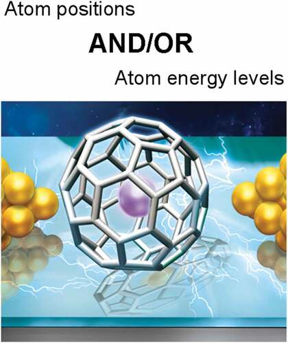
ABSTRACT
The aim of atom electronics, i.e. the final scale of electronics, is to make use of specific individual atoms as active electronic components. Here, we review recent researches on atom electronics in single-molecule transistors (SMTs) through single-atom access and manipulation. We begin by describing the basic concepts and characteristics of atom electronics in SMTs, before discussing some of the most recent examples, including atomic transistors and atomic storage. In our concluding remarks, we discuss some perspectives on fabrication, integration, and other potential atomic devices in which high precision access to, and manipulation of single atoms could be of great significance. This will affect integrated circuits, quantum computing, and other devices that will drive the electronics of the future.
Graphical abstract
1. Introduction to atom electronics
The study of atom electronics relates to the final scale of electronics, and relies on understanding the behavior of individual atoms or small numbers of them [Citation1]. In 1959, Feynman gave a lecture on the idea of manipulating a single atom as a unit of information, as a means of storing the entire Encyclopaedia Britannica [Citation2]. In the 1980s, the invention of the Scanning Tunneling Microscope (STM) made it possible for humans to see and manipulate individual atoms for the first time [Citation3]. Following decades of development, the field of atom electronics is now widely studied, and is expected to extend beyond CMOS electronics in the near future. [Citation1,Citation4–18]
In the 1990s, there were reports of some phenomena related to unpredictable single-atom access in devices as induced by a single donor or trap distributed randomly in an active electronic component [Citation11,Citation12]. Some progress has since been made on the construction of single-atom electronic devices in a more controlled fashion [Citation4,Citation7,Citation8]. The STM technique is probably the most accurate way to manipulate and/or measure a single atom. For example, Fuechsle et al. showed that it was possible to seed individual phosphorus dopant atoms precisely in a silicon substrate using a STM technique [Citation4]. Wyrick et al. at the National Institute of Standards and Technology (NIST), in collaboration with researchers at the University of Maryland, developed a STM lithography method to produce atomic-scale devices [Citation7]. Intriguingly, a single-atom gate was also implemented using the STM technique. The localized charge state of an atom can modulate the charge transport, and even the multi-state of a single molecule [Citation19,Citation20]. Aside from this notable success with the STM technique, Xie et al. developed an alternative way of building a single-atom transistor via the controlled and reversible relocation of one single atom within a metallic quantum point of contact [Citation5,Citation6,Citation9].
Here, we focus on atom electronics in single-molecule transistors (SMTs). We present some basic concepts and key characteristics, before providing some strategies for creating atom electronic devices. Taking atomic storage as a mature example, we describe research efforts ranging from molecular design to atom access and manipulation, and ultimately to the implementation of an atom electronic device. We finish with a brief summary, and provide some perspectives on fabrication, detection, integration, and other potential atomic devices.
2. Atom electronics in single-molecule transistors (SMTs)
2.1 Basic concepts and characteristics
Following early theoretical designs and experimental measurements on molecular devices [Citation21], SMTs have been subject to rapid development in terms of the miniaturization of transistors [Citation22–24]. The ultimate goal of single molecule electronics (SMEs) is the use of molecules as active elements in electronic devices. Over more than half a century of development, SMEs have passed through their novelty phase, and the technology has matured considerably [Citation25–36].
In recent times, SMTs have enabled the establishment of a new platform for the investigation of atom electronics, due to the implementation of single-atom access and manipulation in a molecule, and have opened the way for more complex cascaded molecule circuits in future. One particularly enlightening experimental result is the realization of single-atom transistors by Park et al. at Cornell University, due to access to and successful manipulation of a magnetic atom in a SMT [Citation14].
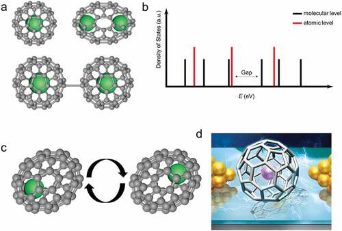
Comparing atom electronics in SMTs with SMEs, the most significant difference is that atom electronics in SMTs use specific atoms in molecules, rather than the molecules themselves, as active electronic elements. Naturally, a molecule consists of a few atoms. In some cases, a specific single atom plays a key role in a SMT. Here, we define molecules of this type as A(atom)@M (molecule), sometimes with an egg-like structure ()). There are at least two characteristics are expected in A@M prior to the implementation of atom electronics in SMTs. The first is that the energy levels of A can be accessed among a range of molecular energy levels ()), and the second is the position of A can be manipulated in the molecule ()). These two characteristics could be used to generate atom electronic signals in SMTs with a high degree of electrical control ()).
Figure 1. The characteristics of atom electronics in SMTs. (a) Structure graphs of A@M molecule, whose structure is like an egg. (b, c) Two characteristics of the realization of atom electronics in SMTs. The first is that the energy levels of a specific atom can be accessed among a range of molecular energy levels. The second is that the position of a specific atom can be manipulated in a molecule. (d) A SMT structure that could detect electronic signals induced by specific atoms with a high electrical controllability.
2.2 Atomic transistors via SMTs
It is generally desirable for the energy levels of a specific atom to be accessed among a range of molecular energy levels, and one practical and feasible way of achieving this is by ensuring that the occupying molecular orbital of the atom is in the frontier orbital, in which the electrons are the most available for chemical reaction. This outcome can be realized by incorporating a magnetic metal atom into a molecule, which can induce a spin-related phenomenon. For example, a single magnetic metal atom might dominate the Kondo effect in a SMT, which originates from an antiferromagnetic coupling between the local magnetic moment of magnetic impurities and conduction electrons.
Generally, the Kondo effect has an odd-even character. When there is an odd number of electrons in a SMT, there is a conductive state at the Fermi level of the electrodes, which results in a differential conductance peak at a zero-bias voltage. Upon addition of an electron, the conductive channel disappears, which results in an off state. Using this principle, it is possible to construct an atomic transistor. Park et al. at Cornell University investigated a single molecule including a Co ion by SMTs [Citation14]. They found that SMTs with longer ligands showed a Coulomb Blockade diamond, while the shorter displayed Kondo peaks referred to a spin 1/2 ground state ()). The Kondo effect is demonstrated by a peak in seen at a bias voltage V = 0 mV with a logarithmic temperature dependence and split under a magnetic field ()). This phenomenon was attributed to the change in the coupling strength between the Co ion and the electrodes. In this case, the single Co atom plays an important part in the transistor while the ligands act as tunneling barriers between the Co atom and the gold electrodes. Park et al. therefore referred to these as single-atom transistors, indicating successful access to and manipulation of a magnetic atom using SMTs.
Figure 2. Atom electronics in SMTs [Citation14,Citation15]. (a, b) Molecules containing a Co atom with long and short linkers used in transistors and the Kondo effect [Citation14]. (c, d) Molecules containing two V atoms in transistors and the Kondo effect [Citation15]. When there is an odd number of electrons in a SMT, there is a conductive state at the Fermi level of the electrodes, which results in a differential conductance peak at a zero-bias voltage.
![Figure 2. Atom electronics in SMTs [Citation14,Citation15]. (a, b) Molecules containing a Co atom with long and short linkers used in transistors and the Kondo effect [Citation14]. (c, d) Molecules containing two V atoms in transistors and the Kondo effect [Citation15]. When there is an odd number of electrons in a SMT, there is a conductive state at the Fermi level of the electrodes, which results in a differential conductance peak at a zero-bias voltage.](/cms/asset/81e84be1-1c03-4d14-acca-42adec031462/tapx_a_2165148_f0002_oc.jpg)
Liang et al. also reported Kondo resonance in SMTs using molecules that contained two vanadium (V) atoms ()) [Citation15]. In ), it is possible to see a clear line at V = 0 mV from the mapping diagram. This is one of the hallmarks of Kondo resonance.
2.3 Atomic storage via SMTs
2.3.1 Molecular design strategies for atomic electrical storage
Endohedral metallofullerenes (EMFs) are a kind of A@M molecule, in which the migration of the atoms inside the carbon sphere has been demonstrated both theoretically and experimentally [Citation37–42]. In 1994, Li and Tománek found that the inner Li atom is confined within a nearly spherical potential well, and exhibits low frequency rotation and high frequency vibrational modes [Citation37]. Bernshtein and Oref further showed that the Li atom is not static but moves around along the walls of the carbon sphere [Citation38]. Through their calculations, they revealed that the Li atom can hop from one ring to another via minimum-energy paths.
Experiments have also been conducted to describe the dynamic behavior of atoms inside fullerenes by X-ray absorption fine structure (XANES) and terahertz (THz) spectroscopy techniques [Citation39–42]. Suzuki et al. observed two peaks in a THz absorption spectrum () [Citation41]; a broad peak at about 1 THz was assigned to the rotation of the Li atom in the carbon sphere, and another sharp peak at about 2.3 THz was assigned to a vibrational mode. The temperature dependence of the two peaks shows that the vibrational mode dominates at low temperatures ().
Figure 3. Rotational and vibrational mode demonstrated using THz absorption spectroscopy[Citation41]. A broad peak at about 1 THz was assigned to the rotation of the Li atom in the carbon sphere, and another sharp peak at about 2.3 THz was assigned to a vibrational mode. The peak at about 1 THz disappears gradually as the temperature is reduced, demonstrating that only the vibrational mode dominates at low temperatures.
![Figure 3. Rotational and vibrational mode demonstrated using THz absorption spectroscopy[Citation41]. A broad peak at about 1 THz was assigned to the rotation of the Li atom in the carbon sphere, and another sharp peak at about 2.3 THz was assigned to a vibrational mode. The peak at about 1 THz disappears gradually as the temperature is reduced, demonstrating that only the vibrational mode dominates at low temperatures.](/cms/asset/73bbb9e8-05d2-453c-8f7a-b9e2f80e2deb/tapx_a_2165148_f0003_oc.jpg)
Aoyagi et al. provided a schematic of the motion of a Li atom inside a carbon sphere by dielectric measurements of [Li@C60](PF6) single crystals () [Citation43]. ) shows the temperature dependence of the real and imaginary parts of the dielectric permittivity. For the imaginary part, as the frequency decreases, the peak position shifts to the low temperature side, which is consistent with previous research [Citation44]. At high temperatures (T > 100 K), the Li atom shows both hopping and tunneling motions ()). While the hopping motion of the Li atom is suppressed when the temperature drops below 100 K, it can still tunnel between two energy minima. The local electric dipole moments can switch as a result of the tunneling motion, a phenomenon proposed for use as qubits in a quantum computer. A phase transition is indicated by a sharp decrease in the real part at 24 K, meaning that at very low temperatures the tunneling motion of the Li atom is also suppressed ()). Therefore, the Li atom may assume either position below 24 K.
Figure 4. Dielectric measurements on a single-molecule dipole[Citation43]. (a) Temperature dependence of the dielectric permittivity of [Li@C60](PF6) single crystals. (b) Schematic of the motion of the Li atom. At T > 100 K, both hopping and tunneling motion of the Li atom occur. At T < 100 K, the hopping motion is suppressed. Below TC, the tunneling motion is suppressed.
![Figure 4. Dielectric measurements on a single-molecule dipole[Citation43]. (a) Temperature dependence of the dielectric permittivity of [Li@C60](PF6) single crystals. (b) Schematic of the motion of the Li atom. At T > 100 K, both hopping and tunneling motion of the Li atom occur. At T < 100 K, the hopping motion is suppressed. Below TC, the tunneling motion is suppressed.](/cms/asset/48df5f15-9890-40bc-bf21-e257d64b5f6f/tapx_a_2165148_f0004_oc.jpg)
To realize the characteristic that the position of a specific atom can be manipulated in a molecule, the fact that the atom can move in the carbon sphere is far from sufficient on its own. In fact, there are at least three other factors at play. First, there is a transition energy barrier between two metastable positions of the inner atom, and intuitively, the inner atom can form two different molecular states. Second, the two different molecular states are polarized, which could be useful for manipulating the position of the atom using a gate voltage. We require the atoms to pass from one stable location to another in a molecule by artificial means. Third, these different molecular states can be distinguished using an electrical method.
Foroutan-Nejad et al. proposed two different molecular states in DM@C70, [Citation45] and an energy barrier between the two states can clearly be seen in ). The red arrow refers to the direction of the single-molecule dipole. ) illustrates how we can switch the direction of the dipole by applying an external electric field. The two polarized states are distinguishable via spectroscopic methods, as infrared radiation (IR) and Raman spectra ()).
Figure 5. Two different polarized molecular states in DM@C70. [Citation45] (a) The existence of a transition barrier between the two states of the inner DM. (b) Schematic representation of the modulation of the direction of the dipole moment by an external electric field. (c, d) IR and Raman spectra of the two states of DM@C70. The two polarized states are distinguishable via spectroscopic methods.
![Figure 5. Two different polarized molecular states in DM@C70. [Citation45] (a) The existence of a transition barrier between the two states of the inner DM. (b) Schematic representation of the modulation of the direction of the dipole moment by an external electric field. (c, d) IR and Raman spectra of the two states of DM@C70. The two polarized states are distinguishable via spectroscopic methods.](/cms/asset/9e21f53f-f29b-4aaa-a321-7d0ebcf737d1/tapx_a_2165148_f0005_oc.jpg)
As well as spectroscopic methods, electron transport studies could also be used to demonstrate different molecular states using single–molecule junctions. This phenomenon was previously shown in STM studies of Sc2@C84 molecules [Citation46]. By considering rotational symmetry, Chandler et al. recently demonstrated 14 molecular states in Li@C60 using the STM technique (5 molecular states demonstrated in dI/dV spectra by experimental means) [Citation47]. They found five kinds of STM images corresponding to precisely five molecular states in Li@C60 ()). They also demonstrated differences in dI/dV spectra corresponding to the five different states ()).
Figure 6. 14 molecular states in a single molecule Li@C60. [Citation47] (a) Five kinds of STM images corresponding to five levels (level 1, 2, 3/4, 5, 6) at −2.5 V (0.1 nA). (b) dI/dV curves of the corresponding five levels. (c) Ball-and-stick model and a deconstructed diagram of Li@C60.
![Figure 6. 14 molecular states in a single molecule Li@C60. [Citation47] (a) Five kinds of STM images corresponding to five levels (level 1, 2, 3/4, 5, 6) at −2.5 V (0.1 nA). (b) dI/dV curves of the corresponding five levels. (c) Ball-and-stick model and a deconstructed diagram of Li@C60.](/cms/asset/41e12823-a734-4ec6-ac62-f89b2a118e64/tapx_a_2165148_f0006_oc.jpg)
2.3.2 Single-atom access and manipulation by voltage
Okamura et al. observed hysteresis in I–V curves together with a change in the Coulomb stability diagram for Ce@C82 SMTs ()) [Citation48]. These results could be related to the reconstruction of the device configuration due to the effect on its electric dipole moment under an external electric field ()). Researchers in our own group, in collaboration with others, choose the Gd@C82 molecule, and found two sets of Coulomb oscillation patterns in Gd@C82 SMTs ())[Citation31]. Initial analysis suggests that the two kinds of patterns originate from two stable molecular states. We plotted the law of switching between the two states at different gate voltages and concluded that there was a ferroelectricity-like hysteresis loop ()).
Figure 7. Electrical measurements on a single-molecule dipole[Citation48]. (a, b) I–V characteristics of a Ce@C82 SMT and a C84 SMT, respectively. (c-f) Coulomb stability diagrams of a Ce@C82 SMT with two possible device configurations.
![Figure 7. Electrical measurements on a single-molecule dipole[Citation48]. (a, b) I–V characteristics of a Ce@C82 SMT and a C84 SMT, respectively. (c-f) Coulomb stability diagrams of a Ce@C82 SMT with two possible device configurations.](/cms/asset/86400bd7-5851-466d-a15c-2bac07ce6f6b/tapx_a_2165148_f0007_oc.jpg)
Figure 8. A Gd@C82 single-molecule electret[Citation31]. (a) Coulomb oscillation patterns in a SMT. (b-c) Schematic of the switching process between the two states. There was a ferroelectricity-like hysteresis loop. (d) The effect on the transition energy barrier between configurations Gd-I and Gd-IV and their stability under gate voltages. (e) The flipping of its electric dipole under gate voltages.
![Figure 8. A Gd@C82 single-molecule electret[Citation31]. (a) Coulomb oscillation patterns in a SMT. (b-c) Schematic of the switching process between the two states. There was a ferroelectricity-like hysteresis loop. (d) The effect on the transition energy barrier between configurations Gd-I and Gd-IV and their stability under gate voltages. (e) The flipping of its electric dipole under gate voltages.](/cms/asset/dbc87576-1e1f-4898-970b-d3431f11a074/tapx_a_2165148_f0008_oc.jpg)
By combining theory with experimental results, the existence of a single-molecule electret has been shown, as discussed in other similar molecular systems [Citation49,Citation50]. From the DFT calculation results in ), a field not only could switch relative stability, but could also reduce the transition energy barrier to zero. Switching of the two states was achieved experimentally by applying a gate voltage of ~10 V, which is close to theoretical expectations.
The role of the gate electric field is to control the dipole flip, which is essentially a position switch for the Gd atom ()). In the same set of experiments, the device was shown to be successful in adjusting the direction of a single-molecule electric dipole by controlling the position of the Gd atom, allowing the creation of a single-molecule electret. This further allowed successful simulation of a two-resistance-state operation, and a new means of miniaturizing storage devices.
2.3.3 New schema of atomic electrical storage
As a basic logical unit, storage is one of the most important elements of the modern electronic industry. Any device with the ability to store, read and write binary information has the potential to be used as storage. Previous studies of atomic electrical storage were based on atomic vacancies in solid-state systems. For example, Kalff et al. reported a rewritable atomic storage using chlorine vacancies on a Cu substrate [Citation51]; another similar study was based on sulfur vacancies in a MoS2 nanosheet [Citation52].
Here, we show two states that exhibited different Coulomb oscillation patterns in Gd@C82 SMTs ()). At some gate voltage points, the currents were significantly different, for one state shows a high current, while another is a blockade. We tested a gate voltage of 7.472 V, and achieved stable operation ()) [Citation31]. In the blockade state, the current was just 2 nA, but after applying a switch gate of +11 V, the current turned to 4 nA, defined as a ‘high’ state. These results are typical for a two-state electret storage device. In this mode of operation, different currents can be defined as different storage states, which could allow the realization of a multi-state nonvolatile storage device if more test voltages are used.
Figure 9. Simulation of a two-state operation in a molecule[Citation31]. (a) The current state switched by applying voltages. The test voltage is 7.472 V. In the blockade state, the current was just 2 nA, but after applying a switch gate of +11 V, the current turned to 4 nA, defined as a ‘high’ state. These results are typical for a two-state electret storage device. (b) The switches of current are stable after a long period of operation.
![Figure 9. Simulation of a two-state operation in a molecule[Citation31]. (a) The current state switched by applying voltages. The test voltage is 7.472 V. In the blockade state, the current was just 2 nA, but after applying a switch gate of +11 V, the current turned to 4 nA, defined as a ‘high’ state. These results are typical for a two-state electret storage device. (b) The switches of current are stable after a long period of operation.](/cms/asset/9f3b8291-d6b7-4e3f-bf88-999dd8987d29/tapx_a_2165148_f0009_oc.jpg)
This operation takes place in a single molecule, which could allow replacement of present storage devices with much smaller counterparts in future. As for the recent description of multiferroics proposed for storage with an extremely high density of 105 Gbit per in [Citation53,Citation54], more physical effects and ideal multiferroics may be expected based on the manipulation of single atoms in a single molecule.
Significantly, the spatial position of the atom is the most critical factor in inducing two different molecular states in the new schema of atomic electrical storage. The barrier between the two molecular states is very important. On the one hand, it should be sufficiently large to prevent spontaneous switching of the initial state via thermal motion. On the other hand, it must be overcome by artificial means.
In summary, it should be possible to design an atomic electrical storage to operate at room temperature through careful design of the barrier. With the arrival of other molecule systems of interest and the maturity of atomic manipulation technology, there will be further interest in the development of knowledge and understanding at the intersection of atom and molecule electronics.
3. Conclusions and perspectives
In this review, we have briefly described the birth of atom electronics in SMTs and discussed recent advances in single atom access and control in SMTs. Combined with recent experimental work undertaken by our group [Citation28,Citation31], we have highlighted some strategies for creating revolutionary atom electronic devices based on SMTs. These devices include atomic transistors and atomic storage. We focused mainly on the manipulation of single atoms in a single molecule and on the improvement of performance brought about by adding or subtracting single atoms in a single molecule. Due to limitations of space, we do not provide an exhaustive description of all related work.
3.1 Perspectives on fabrication, detection, and integration
The related programme of research is in full swing, and important results continue to emerge. However, a range of problems related to the technique remain to be solved as a matter of urgency. For example, the method of electromigration based on metal electrodes means that it is hard to operate SMTs at room temperature, and graphene electrodes may be a more sensible choice. The need for mass production of some special molecules is also important for large-scale SMT research in the future.
We also note the difficulty of positioning a molecule precisely, efficiently, and generally into the nanogap between source and drain. In 2008, Ray et al. reported a method for the parallel fabrication of single-electron devices with a vertical structure, which results in a single-electron device array that operates at room temperature [Citation55]. The interconnection between gold nanoparticles and the oxide wall is realized by a powerful attraction between negative and positive charges using self-assembled monolayers (SAMs) [Citation56,Citation57]. Mirkin and other researchers in his group presented another method for gathering specific metal nanoparticles at electrical junctions via DNA-directed assembly [Citation58]. They stressed that in a single chemical step, this approach could involve assembly of multiple, different nanostructures onto the same chip. This approach has now been demonstrated for positioning high-density carbon nanotube arrays precisely for high performance carbon nanotube transistors [Citation59,Citation60]. In addition to the need to locate a molecule precisely, novel detection and other technologies are also in need of further development.
3.2 Perspectives on other potential atomic devices
3.2.1 Modification of thermoelectric performance of a molecular junction via a single atom
The relationship for the Seebeck coefficient transmission function of a molecular junction (Sjunction) can be obtained as:
Where e is the charge of an electron, kB is the Boltzmann constant, T is the ambient temperature, and is the transmission function [Citation61]. Therefore, Sjunction is related to the slope of
near the Fermi energy, and any molecular engineering that changes the shape of the line of
would have a considerable impact on the thermopower.
The addition, subtraction, or alteration of an atom or group in a molecule can affect the thermoelectric properties, as it could cause a very large slope of , which means that there could be a significant increase in the Seebeck coefficient. Papadopoulos et al. showed that for molecules with side groups ()) [Citation62], the transmission coefficient could be enhanced dramatically by Fano resonances near the Fermi energy, caused by coupling between the side group and the backbone of the molecule. Addition of a side group (for both a single oxygen atom and a bipyridine group) beside the molecule backbone could induce an additional Fano resonance. This Fano transmission function denotes a sharp peak-valley line shape near the Fermi energy, which implies an extremely large slope ()).
Figure 10. Influence of adding side groups into molecular junctions[Citation62]. (a) Structure of molecular with oxygen and bipyridine side group (also named as CSW-479). (b) Comparison between transmission function of the molecule with (solid line) and without (dashed line) an oxygen side group. Addition of a side group beside the molecule backbone could induce an additional Fano resonance. (c) Transmission function of the molecule with bipyridine side group for different twist angles.
![Figure 10. Influence of adding side groups into molecular junctions[Citation62]. (a) Structure of molecular with oxygen and bipyridine side group (also named as CSW-479). (b) Comparison between transmission function of the molecule with (solid line) and without (dashed line) an oxygen side group. Addition of a side group beside the molecule backbone could induce an additional Fano resonance. (c) Transmission function of the molecule with bipyridine side group for different twist angles.](/cms/asset/0e56fc86-7e4c-42f0-b2ce-2a63ccded966/tapx_a_2165148_f0010_b.gif)
Achievement of a high thermopower via a Fano resonance has been investigated and applied widely in different nanodevices [Citation63–67]. The thermoelectric performances of the bipyridine side group molecules mentioned above ()) were also studied by Finch et al [Citation63]., who showed that a large Seebeck coefficient occurs whenever the side group exists, because the Fano resonance can increase the slope of near E = EF by a significant amount. The Seebeck coefficient as a function of temperature and twist angle is shown in ). Compared with the 1,4-biphenyldithiol (BPDT) molecule, CSW-479, which possesses a side group ()), apparently exhibits a far more outstanding thermoelectric capability.
Figure 11. Structure and thermopower of BPDT and CSW-479 molecules[Citation63]. (a) Structure of BPDT and CSW-479. (b, c) Contour plot of the Seebeck coefficient S in CSW-479 and BPDT, respectively. Compared with the BPDT molecule, CSW-479 apparently exhibits a far more outstanding thermoelectric capability.
![Figure 11. Structure and thermopower of BPDT and CSW-479 molecules[Citation63]. (a) Structure of BPDT and CSW-479. (b, c) Contour plot of the Seebeck coefficient S in CSW-479 and BPDT, respectively. Compared with the BPDT molecule, CSW-479 apparently exhibits a far more outstanding thermoelectric capability.](/cms/asset/d7689297-9271-4bcf-a510-192ce51d7489/tapx_a_2165148_f0011_oc.jpg)
3.2.2 Quantum state control in SMTs
In nano-scaled quantum computational devices, the decisive quantum information may rely on the electron or nuclear states of one single atom, i.e. they are the ‘atomtronic qubit’. For example, in research undertaken by Andrea Morello’s group on the qubit based on individual phosphorus donors in silicon for decades [Citation68–71], their three-qubit donor quantum processor was recently reported to have a very high fidelity ()) [Citation71].
Figure 12. The SEM graph (a) and operation procedure (b) of quantum processor based on the phosphorus donor in silicon[Citation71]. The structure (c) and detection architecture (d) of bis(phthalocyaninato)terbium (III) SMM qubit. [Citation73] The organics shell forms a SMT, and the coupling between the SMT and the spin of the terbium (III) ion influences the electron transport, allowing the electrical and nondestructive detection of qubit information.
![Figure 12. The SEM graph (a) and operation procedure (b) of quantum processor based on the phosphorus donor in silicon[Citation71]. The structure (c) and detection architecture (d) of bis(phthalocyaninato)terbium (III) SMM qubit. [Citation73] The organics shell forms a SMT, and the coupling between the SMT and the spin of the terbium (III) ion influences the electron transport, allowing the electrical and nondestructive detection of qubit information.](/cms/asset/265c9d44-d08e-4ba0-acd8-44d197979670/tapx_a_2165148_f0012_oc.jpg)
As for SMT systems, a single atom also could be the quantum information carrier, such as a single-molecule magnet (SMM) with a single metal atom embedded by organics. Wolfgang Wernsdorfer’s group achieved the electrical read-out and control of qubits in a single bis(phthalocyaninato)terbium (III) molecular magnet, whose quantum information is determined by the electronic and nuclear spin of an individual terbium (III) ion [Citation72–76]. The organics shell forms a SMT, and the coupling between the SMT and the spin of the terbium (III) ion influences the electron transport, allowing the electrical and nondestructive detection of qubit information ()) [Citation73].
Here, these single atoms or ions working as qubits are separated and protected by the surrounding shell (silicon or organic molecule), therefore they show a relatively high decoherence time (~100 μs) [Citation73], which is one of the most important aspects of the performance of a qubit. This would be a significant advantage in future quantum computational competition for atom electronics. Last year, Wolfgang Wernsdorfer’s group chose a Tb2Pc3 molecule containing two magnetic centres to construct a Hilbert space with 16 dimensions, opening the way for more developed quantum algorithms [Citation76].
In conclusion, we have described some exciting progress on single atom access and manipulation in SMTs, although it should be emphasized that the research is still in its early stages. More revolutionary mechanisms and functions remain to be discovered, meaning that this field of study could receive significant further research interest and generate wider publicity.
Acknowledgments
We gratefully acknowledge professor Mark Reed for many years of cooperation, and the financial support of the National Key R&D Program of China (No. 2022YFA1402404), the National Natural Science Foundation of China (Grant Nos. 92161201, T2221003, 12104221, 12104220, 12025404 and 12004174), the Natural Science Foundation of Jiangsu Province (Grant Nos. BK20200312 and BK20200310), and the Fundamental Research Funds for the Central Universities (Nos. 020414380192).
Disclosure statement
No potential conflict of interest was reported by the author(s).
Additional information
Funding
References
- Dragoman M, Dragoman D. Atomic-Scale Electronics Beyond CMOS. Cham Switzerland: Springer Nature Switzerland AG; 2021.
- Feynman RP. There’s plenty of room at the bottom. Eng Sci. 1960;23:22–21.
- Binnig G, Rohrer H. Scanning tunneling microscopy. Surf Sci. 1983;126:236–244.
- Fuechsle M, Miwa JA, Mahapatra S, et al. A single-atom transistor. Nat Nanotechnol. 2012;7:242–246.
- Xie F, Nittler L, Obermair C, et al. Gate-controlled atomic quantum switch. Phys Rev Lett. 2004;93:128303.
- Xie F, Maul R, Augenstein A, et al. Independently switchable atomic quantum transistors by reversible contact reconstruction. Nano Lett. 2008;8:4493–4497.
- Wyrick J, Wang X, Kashid RV, et al. Atom-by-atom fabrication of single and few dopant quantum devices. Adv Funct Mater. 2019;29:1903475.
- Wang X, Wyrick J, Kashid RV, et al. Atomic-scale control of tunneling in donor-based devices. Comm Phys. 2020; 3: 82. doi
- Xie F, Peukert A, Bender T, et al. Quasi-solid-state single-atom transistors. Adv Mater. 2018;30:1801225.
- Mol JA, Verduijn J, Levine RD, et al. Integrated logic circuits using single-atom transistors. Proc Nat Aca Sci. 2011;108:13969.
- Dellow MW, Beton PH, Langerak CJGM, et al. Resonant tunneling through the bound states of a single donor atom in a quantum well. Phys Rev Lett. 1992;68:1754–1757.
- Gregory S. Experimental observation of scattering of tunneling electrons by a single magnetic moment. Phys Rev Lett. 1992;68:2070–2073.
- Washburn S. Single atoms as transistors. Nature. 1992;357:199–200.
- Park J, Pasupathy AN, Goldsmith JI, et al. Coulomb blockade and the Kondo effect in single-atom transistors. Nature. 2002;417:722–725.
- Liang W, Shores MP, Bockrath M, et al. Kondo resonance in a single-molecule transistor. Nature. 2002;417:725–729.
- De Franceschi S, Kouwenhoven L. Electronics and the single atom. Nature. 2002;417:701–702.
- Schirm C, Matt M, Pauly F, et al. A current-driven single-atom memory. Nat Nanotechnol. 2013;8:645–648.
- Wang Q, Liu R, Xiang D, et al. Single-atom switches and single-atom gaps using stretched metal nanowires. ACS Nano. 2016;10:9695–9702.
- Martínez-Blanco J, Nacci C, Erwin SC, et al. Gating a single-molecule transistor with individual atoms. Nat Phys. 2015;11:640–644.
- Piva PG, DiLabio GA, Pitters JL, et al. Field regulation of single-molecule conductivity by a charged surface atom. Nature. 2005;435:658–661.
- Aviram A, Ratner MA. Molecular rectifiers. Chem Phys Lett. 1974;29:277–283.
- Reed MA, Zhou C, Muller CJ, et al. Conductance of a molecular junction. Science. 1997;278:252.
- Park H, Park J, Lim AKL, et al. Nanomechanical oscillations in a single-C60 transistor. Nature. 2000;407:57–60.
- Kubatkin S, Danilov A, Hjort M, et al. Single-electron transistor of a single organic molecule with access to several redox states. Nature. 2003;425:698–701.
- Service Robert F. Next-generation technology hits an early midlife crisis. Science. 2003;302:556–559.
- Song H, Kim Y, Jang YH, et al. Observation of molecular orbital gating. Nature. 2009;462:1039–1043.
- Ratner M. A brief history of molecular electronics. Nat Nanotechnol. 2013;8:378–381.
- Bai Z, Liu X, Lian Z, et al. A silicon cluster based single electron transistor with potential room-temperature switching. Chin Phys Lett. 2018;35:037301.
- Jia C, Migliore A, Xin N, et al. Covalently bonded single-molecule junctions with stable and reversible photoswitched conductivity. Science. 2016;352:1443–1445.
- Wagner S, Kisslinger F, Ballmann S, et al. Switching of a coupled spin pair in a single-molecule junction. Nat Nanotechnol. 2013;8:575–579.
- Zhang K, Wang C, Zhang M, et al. A Gd@C82 single-molecule electret. Nat Nanotechnol. 2020;15:1019–1024.
- Gehring P, Sowa JK, Hsu C, et al. Complete mapping of the thermoelectric properties of a single molecule. Nat Nanotechnol. 2021;16:426–430.
- Capozzi B, Xia J, Adak O, et al. Single-molecule diodes with high rectification ratios through environmental control. Nat Nanotechnol. 2015;10:522–527.
- Bai J, Daaoub A, Sangtarash S, et al. Anti-resonance features of destructive quantum interference in single-molecule thiophene junctions achieved by electrochemical gating. Nat Mater. 2019;18:364–369.
- Liu J, Huang X, Wang F, et al. Quantum interference effects in charge transport through single-molecule junctions: detection, manipulation, and application. Acc Chem Res. 2019;52:151–160.
- Greenwald JE, Cameron J, Findlay NJ, et al. Highly nonlinear transport across single-molecule junctions via destructive quantum interference. Nat Nanotechnol. 2021;16:313–317.
- Li YS, Tománek D. How free are encapsulated atoms in C60? Chem Phys Lett. 1994;221:453–458.
- Bernshtein V, Oref I. Surface migrations of endohedral Li+ on the inner wall of C 60. Phys Rev A. 2000;62:033201.
- Liu L, Gao B, Chu W, et al. The structural determination of endohedral metallofullerene Gd@C 82 by XANES. Chem Comm. 2008:474–476. DOI:10.1039/B714603E
- Du S, Zhang Y, Yoshida K, et al. Ultrafast rattling motion of a single atom in a fullerene cage sensed by terahertz spectroscopy. Appl Phys Express. 2020;13:105002.
- Suzuki H, Ishida M, Yamashita M, et al. Rotational dynamics of Li + ions encapsulated in C 60 cages at low temperatures. Phys Chem Chem Phys. 2016;18:31384–31387.
- Kwon E, Komatsu K-I, Kawachi K, et al. Dynamic behavior of lithium-cation in a C 60 fullerene cage elucidated by terahertz spectroscopy. Mol Cryst Liq Cryst. 2014;598:28–31.
- Aoyagi S, Tokumitu A, Sugimoto K, et al. Tunneling motion and antiferroelectric ordering of lithium cations trapped inside carbon cages. J Phys Soc Jpn. 2016;85:094605.
- Zhang M, Harding LB, Gray SK, et al. Quantum states of the endohedral fullerene Li@C 60. J Phys Chem A. 2008;112:5478–5485.
- Foroutan-Nejad C, Andrushchenko V, Straka M. Dipolar molecules inside C 70: an electric field-driven room-temperature single-molecule switch. Phys Chem Chem Phys. 2016;18:32673–32677.
- Shinohara H, Hayashi N, Sato H, et al. Direct STM imaging of spherical endohedral discandium fullerenes (Sc2@C84). J Phys Chem. 1993;97:13438–13440.
- Chandler HJ, Stefanou M, Campbell EEB, et al. Li@C60 as a multi-state molecular switch. Nat Commun. 2019;10:2283.
- Okamura N, Yoshida K, Sakata S, et al. Electron transport in endohedral metallofullerene Ce@C 82 single-molecule transistors. Appl Phys Lett. 2015;106:043108.
- Xinfeng Quan , Geoffrey R. Hutchison. Single molecule ferroelectrics via conformational inversion: an electronic structure investigation. arXiv. 2017;2017:1705.09699.
- Kato C, Machida R, Maruyama R, et al. Giant hysteretic single-molecule electric polarisation switching above room temperature. Angew Chem. 2018;57:13429–13432.
- Kalff FE, Rebergen MP, Fahrenfort E, et al. A kilobyte rewritable atomic memory. Nat Nanotechnol. 2016;11:926–929.
- Hus SM, Ge R, Chen PA, et al. Observation of single-defect memristor in an MoS2 atomic sheet. Nat Nanotechnol. 2021;16:58–62.
- Yang Q, Zhong T, Tu Z, et al. Design of single-molecule multiferroics for efficient ultrahigh-density nonvolatile memories. Adv Sci. 2019;6:1801572.
- Zhong T, Wu M. Fullerene-based 0D ferroelectrics/multiferroics for ultrahigh-density and ultrafast nonvolatile memories. Phys Chem Chem Phys. 2020;22:12039–12043.
- Ray V, Subramanian R, Bhadrachalam P, et al. CMOS-compatible fabrication of room-temperature single-electron devices. Nat Nanotechnol. 2008;3:603–608.
- Smith RK, Lewis PA, Weiss PS. Patterning self-assembled monolayers. Prog Surf Sci. 2004;75:1–68.
- Ma L-C, Subramanian R, Huang H-W, et al. Electrostatic funneling for precise nanoparticle placement: a route to wafer-scale integration. Nano Lett. 2007;7:439–445.
- Chung S-W, Ginger D, Morales M, et al. Top-down meets bottom-up: dip-pen nanolithography and DNA-directed assembly of nanoscale electrical circuits. Small. 2005;1:64–69.
- Zhao M, Chen Y, Wang K, et al. DNA-directed nanofabrication of high-performance carbon nanotube field-effect transistors. Science. 2020;368:878.
- Sun W, Shen J, Zhao Z, et al. Precise pitch-scaling of carbon nanotube arrays within three-dimensional DNA nanotrenches. Science. 2020;368:874.
- Paulsson M, Datta S. Thermoelectric effect in molecular electronics. Phys Rev B. 2003;67:241403.
- Papadopoulos TA, Grace IM, Lambert CJ. Control of electron transport through Fano resonances in molecular wires. Phys Rev B. 2006;74. doi:10.1103/PhysRevB.74.193306
- Finch CM, García-Suárez VM, Lambert CJ. Giant thermopower and figure of merit in single-molecule devices. Phys Rev B. 2009;79:033405.
- Bai J, He Z, Li L, et al. The influence of side-coupled quantum dots on thermoelectric effect of parallel-coupled double quantum dot system. Phys B Condens Matter. 2018;545:377–382.
- Nozaki D, Avdoshenko SM, Sevinçli H, et al. Quantum interference in thermoelectric molecular junctions: a toy model perspective. J Appl Phys. 2014;116:074308.
- Yi W, Lu L, Hu H, et al. Tunneling into multiwalled carbon nanotubes: coulomb blockade and the fano resonance. Phys Rev Lett. 2003;91:076801.
- Kim T-S, Hershfield S. Thermoelectric effects of an Aharonov-Bohm interferometer with an embedded quantum dot in the Kondo regime. Phys Rev B. 2003;67:165313.
- Morello A, Pla JJ, Zwanenburg FA, et al. Single-shot readout of an electron spin in silicon. Nature. 2010;467:687–691.
- Pla JJ, Tan KY, Dehollain JP, et al. High-fidelity readout and control of a nuclear spin qubit in silicon. Nature. 2013;496:334–338.
- Pla JJ, Tan KY, Dehollain JP, et al. A single-atom electron spin qubit in silicon. Nature. 2012;489:541–545.
- Mądzik MT, Asaad S, Youssry A, et al. Precision tomography of a three-qubit donor quantum processor in silicon. Nature. 2022;601:348–353.
- Vincent R, Klyatskaya S, Ruben M, et al. Electronic read-out of a single nuclear spin using a molecular spin transistor. Nature. 2012;488:357–360.
- Thiele S, Balestro F, Ballou R, et al. Electrically driven nuclear spin resonance in single-molecule magnets. Science. 2014;344:1135–1138.
- Godfrin C, Ballou R, Bonet E, et al. Generalized Ramsey interferometry explored with a single nuclear spin qudit. Npj Quantum Inf. 2018;4:53.
- Godfrin C, Thiele S, Ferhat A, et al. Electrical read-out of a single spin using an exchange-coupled quantum dot. ACS Nano. 2017;11:3984–3989.
- Biard H, Moreno-Pineda E, Ruben M, et al. Increasing the Hilbert space dimension using a single coupled molecular spin. Nat Commun. 2021;12:4443.