
 ?Mathematical formulae have been encoded as MathML and are displayed in this HTML version using MathJax in order to improve their display. Uncheck the box to turn MathJax off. This feature requires Javascript. Click on a formula to zoom.
ABSTRACT
Selenium is a chemical element from the chalcogenide group (Oxygen, Sulfur, Selenium and Tellurium), which has been defined as a critical element by the American Physical Society and the Materials Research Society. Indeed, selenium is used abundantly in nanotechnologies but its scarcity on Earth put its sustainability at risk. This review highlights the properties of selenium at the nanoscale and illustrates some of its most important applications in medicine, agriculture, catalysis, opto-electronics, photovoltaics, piezo-electrics and quantum electronics.
GRAPHICAL ABSTRACT

1. Introduction
1.1. Origin and abundance
Selenium was discovered in 1817 in a copper mine in Sweden (Falun Mine), by a Swedish chemist, Berzelius (20 August 1779 – 7 August 1848). Berzelius isolated selenium in his laboratory at the Karolinska Institute in Sweden [Citation1]. He named this new chemical element, selenium, after the Greek Goddess of the Moon, ‘Selene’. The reason behind this name is that selenium shared similar chemical properties with Tellurium, a chemical element discovered in 1782, and named after ‘Tellus’, the Earth Goddess. The similarities between selenium and tellurium can be explained by the fact they both belong to the chalcogenide group (i.e. within the oxygen column of the periodic table: Oxygen (O), Sulfur (S), Selenium (Se) and Tellurium (Te)) in the periodic table of the elements.
Unfortunately, selenium cannot be mined directly because of its scarcity in Earth’s crust. Indeed, its crustal abundance is 0.130 ppm [Citation2]. Consequently, selenium is mainly recovered as a by-product of copper refining. Indeed, the most common minerals containing selenium are copper selenide minerals such as Klockmannite (CuSe) Berzelianite (Cu2Se), Bellidoite (Cu2Se), Umangite (Cu3Se2), and Athabascaite (Cu5Se4). Due to the unevenly distribution of copper ores around the world, only a small number of countries have access to selenium (). Therefore, this situation poses a serious geopolitical risk. This is why in 2011, the US Congress mandated the American Physical Society (APS) and the Materials Research Society (MRS) to establish a list of the most critical chemical elements required to develop energy-related technologies [Citation4,Citation5]. Those chemical elements were coined the term ‘energy-critical elements’ (ECE), and selenium was one of them.
Figure 1. World reserves of selenium (Reproduced with permission from Ref. [Citation3]).
![Figure 1. World reserves of selenium (Reproduced with permission from Ref. [Citation3]).](/cms/asset/320d798c-2280-4997-92e4-91d58310f847/tapx_a_2357809_f0001_oc.jpg)
1.2. Physical and chemical properties
Selenium is a solid material at room temperature but becomes liquid above 221°C. It is chemically stable and does not oxidize at room temperature [Citation6]. Indeed, the affinity of selenium for oxygen is low compared to that of sulfur. Only two types of selenium oxides are known: selenium dioxide (SeO2) and selenium trioxide (SeO3). Selenium dioxide is formed by the combustion of selenium in air. This compound is chemically stable but dissolves in water, giving selenous acid (H2SeO3).
Under normal conditions of temperature and pressure, selenium exists in two varieties: amorphous (orange, red) and trigonal (grey). Selenium is a direct bandgap semiconductor having its energy bandgap falling within the visible range (3.2–1.6 eV); consequently, exhibiting photovoltaic action, where light can be converted directly into electricity. Moreover, selenium also displays photoconductive action, as its electrical resistance decreases with increased illumination [Citation7]. The most important physico-chemical properties of bulk selenium are summarized below in .
Table 1. Properties of bulk selenium.
1.3. Biological properties
In 1957, two research scientists, Klaus Schwarz and Calvin Foltz, both working at the U.S. National Institutes of Health in Bethesda demonstrated that selenium was essential to mammalian life [Citation8]. Indeed, a selenium-deficient diet is associated with diseases [Citation9]. However, it becomes toxic at high concentration. Therefore, selenium has a two-sided effect depending on its concentration (): beneficial at low doses but lethal at high doses.
Figure 2. Biological action of selenium depending on concentration (Reproduced with permission from Ref. [Citation10]).
![Figure 2. Biological action of selenium depending on concentration (Reproduced with permission from Ref. [Citation10]).](/cms/asset/98986490-2d71-4ccb-80a4-79b5e3cd8d13/tapx_a_2357809_f0002_oc.jpg)
The two sources of selenium for mammalian cells are selenite (SeO3−2) and selenate (SeO4−2) from food and water. Selenium is consequently mainly absorbed in the duodenum and caecum by active transport through a sodium pump [Citation6]. The biological function of selenium is then exerted through selenoproteins, the main one being selenocysteine encoded by the TGA codon [Citation11]. In total, there are 25 selenoproteins encoded in the human genome [Citation12].
2. Size matters: from bulk to nano
Like any other material, selenium undergoes size and shape effects when its size is shrunk to the nanometer scale [Citation13,Citation14]. There are two type of size effects: one related to the surface effects and the other one related to quantum effects [Citation15].
2.1. Surface effects
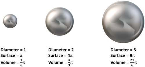
Let’s assume having a spherical nanoparticle with a diameter D. For a sphere, its surface area and volume are given by A=πD2 and V = 1/6πD3, respectively; therefore, the surface to volume ratio (A/V) is given by A/V = 6/D. Consequently, A/V scales inversely with the size of the particle. Therefore, when the size (D) of a particle decreases, its surface to volume (A/V) ratio increases (). Having more surface atoms than core atoms are responsible for the surface effects because the atoms present at the surface have fewer neighbors than in the bulk.
Figure 3. Sketch illustrating the effect of size on the surface to volume ratio.
The size-dependency due to surface effects can be calculated by using some thermodynamics. Indeed, it has been found by Guisbiers [Citation14] that all size-dependent material properties can be described by using the following scaling law:
where ξ represents the size/shape-dependent material property and represents the bulk material property, S represents the type of quantum statistics i.e. either Fermi-Dirac (S = ±1/2) or Bose-Einstein (S = ±1).
is defined as
; where A/V is the surface-to-volume ratio,
is the bulk melting enthalpy, and
and
are the surface energies in the liquid and solid states, respectively. Physically,
quantifies the magnitude of the size effect.
2.2. Quantum effects
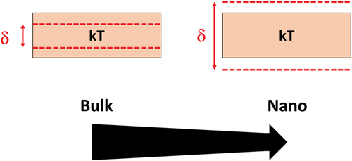
When the size of the material, selenium in this case, is reduced, less energy levels are required to accommodate all the electrons of each selenium atom as compared to the bulk situation. Since, the energy levels are split between the ground level and the Fermi level;however, as less energy levels are required, the energy gap between two successive energy levels, δ, increases. If the level spacing, δ, is larger than the thermal energy, kT, then quantum confinement can be observed () [Citation16]. If the level spacing, δ, is smaller than the thermal energy, kT, then the energy levels look continuous and not discrete. According to quantum mechanics, electrons can be described as ‘particles in a box’, and the energies of those ‘particles’ depend crucially on the size of the box i.e. the size of your (nano)material.
Figure 4. Sketch of two successive energy levels in a bulk material and in a nanomaterial.
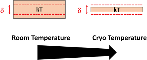
The other option to exhibit the quantification of energy levels is to work at cryogenic temperature. If the size of the material does not change, δ is fixed; therefore, to see the quantification kT needs to be reduced ().
Figure 5. Sketch of two successive energy levels at room temperature versus at cryogenic temperature.
If selenium absorbs a photon with energy at least equal to the fundamental energy band gap, an electron can be promoted from the highest valence energy level to the lowest conduction energy level; consequently, forming an electron-hole pair that can be described as a quasi-particle called exciton. The electron in the conduction band is described by a negative charge (e−), with an effective mass (me*), whereas the hole in the valence band is characterized by a positive charge (h+) with an effective mass (mh*). The effective mass reflects the increased or decreased mobility of a charge carrier (electron or hole) in a semiconductor with respect to that of an electron in vacuum (). Indeed, in contrast to a free electron traveling through vacuum, electrons/holes in a semiconductor experience a potential caused by the atoms within the semiconductor. Therefore, an effective mass larger than the free electron mass (m0) corresponds to a slower charge carrier, whereas a smaller effective mass represents a faster charge carrier.
Table 2. Quantum confinement.
By analogy to the hydrogen atom, the distance between the electron and hole in an exciton is called the exciton Bohr radius. It is interesting to note that the exciton Bohr radius and the energy band gap of the semiconductor are correlated, so that materials with wider energy band gaps possess smaller Exciton Bohr radius [Citation17]. With a bulk energy bandgap of 1.79 eV, selenium displays an Exciton Bohr radius of ~5.0 nm (), meaning that any particle with a diameter less than ~10 nm will exhibit quantum confinement. Indeed, the spatial confinement of excitons within a semiconductor nanostructure leads to a phenomenon known as quantum confinement. For your information, there is a wide range of values for the effective mass in the literature, which consequently can lead to different values of Bohr radius as the ones indicated in .
3. Nano selenium
3.1. Size effects on thermal properties of Se
The melting temperature of selenium, i.e. the temperature at which selenium changes its state from solid to liquid, varies with its size. At the bulk scale, the melting temperature of Se is 221°C, as indicated in . However, when the size of selenium shrinks to the nanometer scale, its melting temperature decreases as shown in . Moreover, the transition temperature from amorphous to trigonal is also size-dependent as it can be seen from .
Figure 6. Size-dependent melting temperature of Se (Adapted with permission from Ref. [Citation21]).
![Figure 6. Size-dependent melting temperature of Se (Adapted with permission from Ref. [Citation21]).](/cms/asset/f99368e8-6cb0-48d1-8f9d-2e68ce6f73dc/tapx_a_2357809_f0006_oc.jpg)
At the melting temperature, the change in the Gibbs free energy is zero and both phases, solid and liquid, co-exist. The size-dependency of the melting temperature () can be calculated like:
Similar relationships were obtained by Buffat et al. [Citation22], Couchman et al. [Citation23], Skripov et al. [Citation24], Sun et al. [Citation25], Qi [Citation26], Zhang et al. [Citation27]. For more details, please read the following reviews [Citation28,Citation29].
The Debye temperature, , of selenium is the temperature of selenium’s highest normal mode of vibration
, and it correlates its elastic properties with the thermodynamic properties of selenium such as phonons. Indeed, the Debye temperature is defined as
. At frequencies
higher than
, the lattice is unable to see the thermal vibrations within selenium because the wavelength of the thermal vibration is smaller than the atomic unit cell of selenium (). Consequently, the Debye temperature separates the collective thermal lattice vibration (classical world) from the independent thermal lattice vibration (quantum world) [Citation31].
Table 3. Unit cell parameters and Debye cut-off values.
The size-dependency of the Debye Temperature () can be calculated as:
Figure 7. Size-dependent Debye temperature of Se (Reproduced with permission from Ref. [Citation3]).
![Figure 7. Size-dependent Debye temperature of Se (Reproduced with permission from Ref. [Citation3]).](/cms/asset/2f7df113-550f-4c1a-8ff4-e0e2042ddce6/tapx_a_2357809_f0007_oc.jpg)
Similar models were developed by Ma et al. [Citation32], Yang et al. [Citation33], Jiang et al. [Citation34], Zhu et al. [Citation35], Ansari [Citation36], and Sun [Citation37].
The thermal expansion coefficient, , of selenium describes how the size of an object changes with a change in temperature. It refers to the rate at which selenium expands with increase in temperature. This coefficient also varies with size. The thermal expansion coefficient increases when the size is reduced. The size-dependency of the thermal expansion coefficient () can be calculated by:
Figure 8. Size-dependent thermal expansion coefficient of selenium (Reproduced with permission from Ref. [Citation40,Citation41])..
![Figure 8. Size-dependent thermal expansion coefficient of selenium (Reproduced with permission from Ref. [Citation40,Citation41])..](/cms/asset/245209fa-0bbf-48fc-a454-674813de34be/tapx_a_2357809_f0008_b.gif)
Similar models were also developed by Goyal et al. [Citation38,Citation39], Yang et al. [Citation33], and Sun [Citation37].
3.2. Size effects on optical properties of Se
The energy bandgap, Eg, of a semiconductor can also be predicted by using thermodynamic concepts. Indeed, the energy bandgap can be described as the variation of the Gibbs free energy between the conduction and valence energy bands, namely, , where
and
are the variation of enthalpy and entropy between the conduction and valence energy bands, respectively [Citation42–44]. At the nanoscale, the energy bandgap increased when the size of the semiconductor is reduced [Citation14].
The size dependency of the energy bandgap () can be calculated by:
Figure 9. Size-dependent Energy bandgap of Se (Reproduced with permission from Ref. [Citation45]).
![Figure 9. Size-dependent Energy bandgap of Se (Reproduced with permission from Ref. [Citation45]).](/cms/asset/b1bb846d-05a9-4ae0-87fe-61629b72a40f/tapx_a_2357809_f0009_oc.jpg)
A similar model was also developed by Singh et al. [Citation46,Citation47], Goyal et al. [Citation48,Citation49]. According to Chaturvedi and Goyal [Citation50], Guisbiers’ model is found best out of the models considered to study the band gap expansion in semiconducting nanomaterial compounds.
4. Synthesis
4.1. Via chemical routes
Over the past 30 years, chemical synthesis has been considered the gold standard for the synthesis of selenium nanoparticles [Citation51]. It is based on the chemical reduction of selenium salts. Generally, selenium nanoparticles can be synthesized by reducing sodium selenite (Na2SeO3) with ascorbic acid (vitamin C) as a reducing agent and Triton X-100 as the stabilizing agent [Citation52]. Polysorbate 20, protic acid, lysozyme can also be used as stabilizing agent [Citation53–55]. Selenium nanoparticles can also be produced by the reaction of ionic liquid (3-methylimidazolinium methane sulfonate) with sodium selenosulphate (Na2SeSO3) a selenium precursor, in the presence of polyvinyl alcohol stabilizer, in aqueous medium [Citation56].
Elongated selenium nanostructures can be synthesized by wet-chemical reactions. Indeed, selenium nanowires were obtained by mixing selenium dioxide (SeO2) in aqueous solution at room temperature with ascorbic acid (vitamin C) and β-cyclodextrin [Citation57]. Selenium nanorods were obtained by wet-chemical reaction of selenous acid (H2SeO3) and L-Cysteine as reducing agent and soft template at room temperature and high intensity ultrasonication [Citation58]. To explain the uni-dimensional growth of the selenium nanostructures, an oriented growth mechanism was proposed by Chen et al. [Citation58] similar to the one proposed by Gedanken [Citation59]. Indeed, sonication involves the creation, growth and collapse of acoustic bubbles. During the collapse, chemical bonds were broken. By increasing the sonication time, aggregation occurred and the shape of selenium nanostructures evolved from nanospheres to nanorods by oriented aggregation. Selenium is apt to grow into 1D nanostructure because of its unique property to grow anisotropically [Citation60].
4.2. Via biological routes
Biosynthesis of selenium nanoparticles can be realized in two ways: ① directly by using living micro-organisms (bacteria, fungi, yeast) or ② with the help of bioreagents extracted from plants. It usually involves adding microorganisms or plant extracts to a sodium selenite solution (Na2SeO3), or a sodium selenate solution (Na2SeO4), or a solution of selenous acid (H2SeO3) or a solution containing selenium dioxide (SeO2) [Citation61].
The micro-organisms reduce selenium by using their own metabolism [Citation51]. The reduction of selenite (SeO32−) and selenate (SeO42−) oxyanions into elemental selenium (Se0) is one of the mechanisms used by microorganisms to remove toxic Se-based oxyanions in aerobic and anaerobic conditions [Citation62]. Indeed, selenium is a double-edge sword chemical element, essential within a small concentration range and toxic at higher concentration. Therefore, some microorganisms have evolved to eliminate selenium by forming elemental selenium nanoparticles (Se0). The formation of selenium nanoparticles by microorganisms depends also on several external conditions such as selenium addition method, culture temperature, pH value, culture medium, oxygen flux, selenium source, and exogenous ions [Citation51]. Generally, the formation of selenium nanoparticles by microorganisms is accompanied by the presence of organic substances on the surface of selenium nanoparticles.
Any part of the plant, such as fruits, leaves, stems, or nuts, can be crushed and used as plant extract. The extract is then being added into varying concentrations of selenium-based solutions. Plants extracts act as reducing agents, which are electron donors for selenium oxyanions, to consequently convert them into selenium nanoparticles. With plant extracts, selenium nanoparticles can be produced without requiring any specific equipment [Citation63].
4.3. Via physical routes
Pulsed laser ablation in liquids (PLAL) is an approach to produce micro-/nanostructure directly from bulk materials [Citation64]. Generally, a nanosecond laser is used to irradiate the target. To create selenium nanoparticles, a target made of bulk Se pellets [Citation65] (99.999% from Sigma-Aldrich) or Se powder [Citation66] (99.999% from Alfa Aesar) can be used. Se target is then placed inside a container such as a 50 ml rounded single-neck glass flask. The solvent is then poured in the container to cover the target. If the laser beam hits the Se target from above, it is called a ‘Top-ablation’ synthesis protocol () while if it hits the Se target from underneath the container, it is called a ‘Bottom-ablation’ synthesis protocol (). The laser beam is reflected onto a flat mirror, inclined at 45° with respect to the laser rail. After being reflected, the laser beam is focused by a biconvex lens onto the Se target. The choice of the focal length depends on the synthesis protocol.
Let’s summarize the effects of the PLAL parameters on the size, shape, and phase of the Se nanoparticles into . In order to get smaller nanoparticles, irradiating a powder is more advantageous compared to a bulk target such as pellets for the same irradiation time. Smaller Se nanoparticles can be obtained by adding some surfactants to the solvent, such as Cetyltrimethylammonium bromide (CTAB) or Sodium dodecyl sulfate (SDS) [Citation66]. To get spherical nanoparticles, deionized water [Citation65] is generally chosen as the preferred solvent while for non-spherical nanostructures, organic solvents [Citation67], such as acetone, ethanol, methanol, hexane or toluene, are preferred. If the solvent is fixed, increasing the pulse repetition rate will help to increasing the aspect ratio of the nanostructure [Citation67]. At room temperature, amorphous Se nanoparticles are obtained while at higher temperatures (≥70°C) trigonal Se nanoparticles are obtained.
Figure 10. Pulsed Laser Ablation in Liquids (PLAL) set-up: a) Top-ablation synthesis protocol, b) Bottom-ablation synthesis protocol.
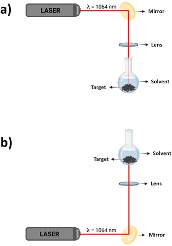
Table 4. Correlations between size, shape, phase of the nanoparticles with the PLAL parameters.
4.4. Conclusions
The advantages and disadvantages of the synthesis protocols discussed above have been summarized in .
Table 5. Comparison between synthesis methods.
5. Applications
5.1. Medical applications
Selenium is recognized as an essential nutrient for living organisms. It is found in selenoproteins synthesized by the selenium metabolic system. Selenoproteins have a wide range of cellular functions including selenium transport within the organism, production of thyroid hormones, function of the immune system, and redox homeostasis. Deficiency of selenium within living organisms lead to diseases [Citation68]. During the recent coronavirus disease 2019 (COVID-19) pandemic, a higher incidence of mortality has been found for patients showing a deficiency in selenium [Citation69,Citation70].
Moreover, selenium is also known to exhibit antibacterial [Citation65], antifungal [Citation21], antiviral [Citation69,Citation71,Citation72] and anticancer [Citation65,Citation73] properties, especially at the nanoscale. Indeed, selenium nanoparticles exhibits a strong antimicrobial activity, due to their huge surface to volume ratio. Se NPs antimicrobial activity can be described by three main mechanisms: (1) impairing cell walls and membranes [Citation74,Citation75]; (2) penetrating through cell membranes and subsequent interference in the activities of biological molecules [Citation21,Citation75]; and (3) increasing oxidative stress [Citation45,Citation65]. The anti-cancer property is also related to the production of reactive oxygen species (ROS) [Citation45,Citation73]. It is well known that an increase in the cellular ROS induces apoptosis, which ultimately causes cell death.
5.2. Agricultural applications
Selenium is also a key element in agriculture where it has been used mainly in three areas: pre-production (seeding & feeding), production (planting & farming) and post-production (processing & distributing) [Citation76].
The presence of selenium in the soil is a result of the weathering of Se-based minerals, volcanic activity, coal burning facilities, some fertilizers, and some water sources. In the United States, the major seleniferous areas can be found in Montana, North and South Dakota, Wyoming, Colorado, and Utah [Citation77]. Generally, the soil is classified as Se-rich if the selenium concentration is higher than 4 mg/kg; or as Se-deficient if the selenium concentration is less than 0.5 mg/kg. Worldwide, most of the soil is classified as Se-deficient. To remediate to the low concentration of selenium in soils, some countries such as Finland, incorporated selenium (in the form of selenate) into fertilizers since 1984 [Citation78]. Selenium enters the food system, through plants and soil microorganisms, which can take up selenium into their proteins. But, selenium can also be added manually to the alimentation of livestock. Indeed, livestock feed are primarily plant‐based with added nutrient supplements such as selenium. Se treatment can also be applied on fruits before being harvest to improve the storability of fruits and other horticultural crops [Citation76].
5.3. Catalytic applications
Selenium is a semiconductor displaying an energy bandgap of 1.79 eV at the bulk scale. However, it exhibits a much larger value at the nanoscale, depending on the size of the nanoparticle [Citation79]. Consequently, Se nanoparticles mainly absorbs the sunlight in the UV and visible regions, and can be used as a photocatalyst to degrade organic pollutants in wastewater.
Most of the pollutants are dyes used in the textile, cosmetic, food and pharmaceutical industries. Rhodamine B dye, one of the most toxic dye in the textile industry, can be degraded by Se nanoparticles under a UV-A light [Citation80]. Methylene blue is another dye abundantly used in the textile industry [Citation81]. The photocatalytic decomposition of Methylene blue by Se NPs was reported by Iqbal et al. [Citation82] and Fouda et al. [Citation83]. The Fuchsin dye, also used in the textile industry, can be completely degraded by Se nanoparticles as shown by Al Jadhaly et al. [Citation84] ().
Figure 11. Organic dyes from the textile industry that can be degraded by Se nanoparticles (Adapted with permission from Ref. [Citation85]).
![Figure 11. Organic dyes from the textile industry that can be degraded by Se nanoparticles (Adapted with permission from Ref. [Citation85]).](/cms/asset/a9f97695-0133-406c-a531-f17f410b3470/tapx_a_2357809_f0011_b.gif)
5.4. Photocell applications
The photoconductivity of Se was firstly discovered by an English engineer, Willoughby Smith, in 1873 [Citation86]. A photocell or photoresistor is a sensor that changes its resistance when light shines on it. Indeed, a photocell operates on semiconductor photoconductivity i.e. when the photons hit the semiconductor, the free electrons, consequently, decreasing the resistance. A high intensity of photons on the semiconductor will cause a lower resistance, while a lower intensity of photons will cause a higher resistance. Therefore, due to its high photoconductivity (~8×10⁴ Scm−1) [Citation57,Citation87], selenium is used in high-tech applications such as sensors, rectifiers, and xerography [Citation88].
5.5. Photovoltaic applications
In 1877, a Professor from the King’s College in London, William Grylls Adams and his student, Richard Evans Day, observed for the first time the photovoltaic effect in selenium; i.e. selenium produces an electric current when light strikes it [Citation89]. In 1883, the first solar cell was made of selenium by an American inventor, Charles Fritts [Citation90]. The solar cell was less than 1% efficient at converting sunlight into electricity and thus not very practical. Some research on selenium photovoltaics continued for the next several decades, but selenium research declined in the wake of the rapidly expanding silicon microelectronic industry which offered a high-quality material with an energy band gap more suitable for a single junction solar cell. Up to now, the best conversion efficiency for a selenium solar cell was achieved in 2017 by Todorov et al. with 6.51% [Citation91].
5.6. Piezoelectric applications
The piezoelectric effect appears in crystals when subjected to pressure, a potential difference appears between their two end faces. This does not happen in all crystals but in most non-centrosymmetric crystals (i.e. lacks inversion symmetry). Selenium is known to be a piezoelectric material at the bulk scale [Citation92–96]. And, its piezoelectric properties are preserved at the nanoscale. Indeed, the trigonal structure of selenium (t-Se) has an anisotropic crystal lattice where individual helical chains of Se atoms are stacked together by weak bonding [Citation95]. Each Se atom is covalently bonded with its two nearest neighbours on the same chain (intrachain bonding) [Citation97]. The interchain bonding is partly Van der Waals in character with an admixture of some covalent bonding. Consequently, Se nanowires exhibit strong piezoelectric properties due to the anisotropic crystal structure of the trigonal phase [Citation97–99].
5.7. Quantum applications
5.7.1. Quantum dots (0D)
Quantum dots (QDs) are semiconductor nanoparticles physically confined in all three dimensions, which result in discrete energy levels and increased energy bandgap such that QDs commonly have different fluorescent properties from their bulk counterpart [Citation100]. Selenium quantum dots (Se QDs) can be synthesized by ultrasound Liquid-Phase Exfoliation (LPE) using Se or NbSe2 powders as the source material and N-Methyl-2-pyrrolidone (NMP) as the dispersant [Citation101,Citation102]. Se QDs can also be prepared by pulsed laser ablation in liquids, i.e. irradiating a selenium target totally submerged in de-ionized water with a nanosecond laser [Citation65,Citation103,Citation104]. Se QDs find wide application in medicine, particularly in bioimaging, and biosensing. Indeed, the advantage of Se QDs compared to metal-based Se QDs such as cadmium selenide QDs or lead selenide QDs, is that without the presence of heavy metal ions, Se QDs have a lower cytotoxicity [Citation100].
5.7.2. Quantum wires (1D)
Selenium has a strong tendency to grow into nanowires due to its anisotropic atomic structure. A solution-phase approach to the large-scale synthesis of uniform nanowires of trigonal selenium (t-Se) with lateral dimensions controllable in the range of ~ 10 to ~800 nm, and lengths up to hundreds of microns was developed by Gates et al. [Citation87,Citation105]
t-Se nanowires having a width of 70–100 nm and length up to tens of microns were synthesized in absolute ethanol at room temperature [Citation106]. The synthesis of Se nanowires with a mean diameter around 65 nm can also be realized in aqueous solution at room temperature by using ascorbic acid (vitamin C) as the reducing agent under the assistance of β-cyclodextrin [Citation57]. In order for those nanowires to exhibit quantum properties, the diameter needs to be less than ~10 nm [Citation17].
5.7.3. Quantum film (2D)
Two-dimensional (2D) selenium, called ‘Selenene’, has become a new member of the 2D Xenes semiconducting nanomaterial families in 2017 [Citation107]. It was synthesized through LPE by Xing et al. [Citation108] who obtained for the first time, 2D Se nanosheets with 40–120 nm in lateral dimension and 3–6 nm in thickness. The sheets composed of well-aligned one-dimensional Se atomic chains bonded via Van der Waals (VdW) interactions [Citation109]. 2D Se nanosheets can also be synthesized by Chemical Vapor Transport (CVT) and Physical Vapor Deposition (PVD) methods, with a thickness than could be as thin as 0.75 nm and 5 nm, respectively [Citation110,Citation111].
6. Conclusions
Selenium is a key chemical element in nanotechnology by displaying amazing bio-physico-chemical properties at the nanoscale. Current applications include medical, agricultural, catalytic, photocell, photovoltaic, piezoelectric and quantum applications. Those applications rely on some particular properties of selenium. The most important ones since the discovery of this chalcogenide element are summarized into . Based on this table, it is noticed that selenium quantum nanowires (1D) still need to be synthesized by experimentalists; the challenge seems to be the diameter of the nanowire being currently too large to exhibit quantum properties. For the most part, the solution-based approaches (chemical and biological routes), exploit noxious raw materials such as Na2SeO3 and H2SeO3; while the physical routes involve pure selenium targets. From this review, it is clear that selenium will continue to be a major player in future nano/quantum technologies.
Table 6. Key events in selenium history.
Funding
The work was supported by the National Science Foundation [2228891].
Disclosure statement
No potential conflict of interest was reported by the author(s).
Data availability statement
Data sharing is not applicable to this article as no new data were created or analyzed in this study.
Additional information
Funding
References
- Trofast J. Berzelius’ discovery of selenium. Chem Int. 2011 Sep-Oct;33(5):16–19.
- https://www.rsc.org/periodic-table/element/34/selenium
- Geoffrion LD, Guisbiers G. Physico-chemical properties of selenium–tellurium alloys across the scales. Nanoscale Adv. 2021;3:4254–4270. doi: 10.1039/D1NA00087J
- Jaffe R, Price J, Ceder G, et al. APS/MRS Report. 2011.
- Hurd AJ, Kelley RL, Eggert RG, et al. Energy-critical elements for sustainable development. MRS Bull. 2012;37:405–410. doi: 10.1557/mrs.2012.54
- Mehdi Y, Hornick JL, Istasse L, et al. Selenium in the environment, metabolism and involvement in body functions. Molecules. 2013;18:3292–3311. doi: 10.3390/molecules18033292
- Zhu M, Niu G, Tang J. Elemental Se: fundamentals and its optoelectronic applications. J Mater Chem C. 2019;7:2199–2206. doi: 10.1039/C8TC05873C
- Schwarz K, Foltz CM. Selenium as an integral part of factor 3 against dietary necrotic liver degeneration. J Am Chem Soc. 1957;79:3292–3293. doi: 10.1021/ja01569a087
- Lee KH, Jeong D. Bimodal actions of selenium essential for antioxidant and toxic pro-oxidant activities: the selenium paradox (Review). Mol Med Rep. 2012;5:299–304. doi: 10.3892/mmr.2011.651
- Razaghi A, Poorebrahim M, Sarhan D, et al. Selenium stimulates the antitumour immunity: Insights to future research. Eur J Cancer. 2021;155:256–267. doi: 10.1016/j.ejca.2021.07.013
- Lu J, Holmgren A. Selenoproteins. J Biol Chem. 2009;284:723–727. doi: 10.1074/jbc.R800045200
- Kurokawa S, Berry MJ. Interrelations between essential metal ions and human diseases. In: Sigel A, Sigel H, and Sigel R, editors. Metal ions in life sciences. Vol. 13. Dordrecht: Springer; 2013. p. 499–534.
- Guisbiers G, Mejia-Rosales S, Deepak FL. Nanomaterial properties: size and shape dependencies. J Nanomater. 2012;2012:1–2. doi: 10.1155/2012/180976
- Guisbiers G. Advances in thermodynamic modelling of nanoparticles. Adv Phys: X. 2019;4:1668299. doi: 10.1080/23746149.2019.1668299
- Roduner E. Size matters: why nanomaterials are different. Chem Soc Rev. 2006;35:583–592. doi: 10.1039/b502142c
- Halperin WP. Quantum size effects in metal particles. Rev Mod Phys. 1986;58:533–606. doi: 10.1103/RevModPhys.58.533
- Geoffrion LD, Guisbiers G. Quantum confinement: size on the grill!. J Phys Chem Solids. 2020;140:109320. doi: 10.1016/j.jpcs.2019.109320
- Siemsen KJ, Fenton EW. Optical absorption by excitons in amorphous selenium. Phys Rev. 1967;161:632–636. doi: 10.1103/PhysRev.161.632
- Johnson JA, Saboungi M-L, Thiyagarajan P, et al. Selenium nanoparticles: a small-angle neutron scattering study. J Phys Chem B. 1999;103:59–63. doi: 10.1021/jp983229y
- Beyer W, Mell H, Stuke J. Conductivity and thermoelectric power of trigonal Se x Te 1− x single crystals. Phys Status Solidi B. 1971;45:153. doi: 10.1002/pssb.2220450116
- Guisbiers G, Lara HH, Mendoza-Cruz R, et al. Inhibition of Candida albicans biofilm by pure selenium nanoparticles synthesized by pulsed laser ablation in liquids. Nanomed Nanotechnol Biol Med. 2017;13:1095–1103. doi: 10.1016/j.nano.2016.10.011
- Buffat P, Borel J-P. Size effect on the melting temperature of gold particles. Phys Rev A. 1976;13:2287. doi: 10.1103/PhysRevA.13.2287
- Couchman PR, Jesser WA. Thermodynamic theory of size dependence of melting temperature in metals. Nature. 1977;269:481–483. doi: 10.1038/269481a0
- Skripov VP, Koverda VP, Skokov VN. Size effect on melting of small particles. Phys Status Solidi A. 1981;66:109–118. doi: 10.1002/pssa.2210660111
- Sun CQ, Tay BK, Zeng XT, et al. Bond-order bond-length bond-strength (bond-OLS) correlation mechanism for the shape-and-size dependence of a nanosolid. J Phys. 2002;14:7781. doi: 10.1088/0953-8984/14/34/301
- Qi WH. Size effect on melting temperature of nanosolids. Phys B Condens Matter. 2005;368:46–50. doi: 10.1016/j.physb.2005.06.035
- Zhang X, Li W, Wu D, et al. Size and shape dependent melting temperature of metallic nanomaterials. J Phys. 2018;31:075701. doi: 10.1088/1361-648X/aaf54b
- Guisbiers G. Review on the analytical models describing melting at the nanoscale. J Nanosci Lett. 2012;2:8.
- Nanda KK. Size-dependent melting of nanoparticles: Hundred years of thermodynamic model. Pramana. 2009;72:617–628. doi: 10.1007/s12043-009-0055-2
- https://www.webelements.com/selenium/
- Garai J. ArXiv Preprint Physics. 2007. Available from: https://arxiv.org/ftp/physics/papers/0703/0703001.pdf, 0703001
- Ma Y-L, Zhu K, Li M. Size, dimensionality and composition effects on the Debye temperature of nanocrystals. Phys Chem Chem Phys. 2018;20:27539–27544. doi: 10.1039/C8CP04935A
- Yang CC, Xiao MX, Li W, et al. Size effects on Debye temperature, Einstein temperature, and volume thermal expansion coefficient of nanocrystals. Solid State Commun. 2006;139:148–152. doi: 10.1016/j.ssc.2006.05.035
- Jiang X, Sheng H, Xiao B. Size effect on Debye temperature of metal crystals. Phys Chem Chem Phys. 2023;25:29310–29314. doi: 10.1039/D3CP04236G
- Zhu YF, Lian JS, Jiang Q. Modeling of the melting point, debye temperature, thermal expansion coefficient, and the specific heat of nanostructured materials. J Phys Chem C. 2009;113:16896–16900. doi: 10.1021/jp902097f
- Ansari MA. Modelling of size-dependent thermodynamic properties of metallic nanocrystals based on modified Gibbs–Thomson equation. Appl Phys A. 2021;127:385. doi: 10.1007/s00339-021-04535-4
- Sun CQ. Thermo-mechanical behavior of low-dimensional systems: The local bond average approach. Pro Mater Sci. 2009;54:179–307. doi: 10.1016/j.pmatsci.2008.08.001
- Goyal M, Gupta BRK. Study of shape, size and temperature-dependent elastic properties of nanomaterials. Mod Phys Lett B. 2019;33:1950310. doi: 10.1142/S021798491950310X
- Goyal M, Gupta BRK. Shape, size and temperature dependency of thermal expansion, lattice parameter and bulk modulus in nanomaterials. Pramana. 2018;90:80. doi: 10.1007/s12043-018-1563-8
- Guisbiers G. Size and shape dependencies of nanomaterial properties: thermodynamic considerations. Symp Proc. 2012;1371:1371. doi: 10.1557/opl.2012.153
- Guisbiers G, Arscott S, Gaudet M, etal. Selenium surface energy determination from size-dependent considerations. In: Proceedings - 2013 IEEE 5th International Nanoelectronics Conference (INEC); Singapore; 2013. p. 105–109.
- Van Vechten JA, Wautelet M. Variation of semiconductor band gaps with lattice temperature and with carrier temperature when these are not equal. Phys Rev B. 1981;23:5543. doi: 10.1103/PhysRevB.23.5543
- Wautelet M, Van Vechten JA. Carrier diffusion in semiconductors subject to large gradients of excited carrier density. Phys Rev B. 1981;23:5551. doi: 10.1103/PhysRevB.23.5551
- Guisbiers G, Wautelet M, Buchaillot L. Phase diagrams and optical properties of phosphide, arsenide, and antimonide binary and ternary III-V nanoalloys. Phys Rev B. 2009;79:155426. doi: 10.1103/PhysRevB.79.155426
- Medina-Cruz D, Mostafavi E, Vernet-Crua A, etal. Chapter 12 - Green nanotechnology and nanoselenium for biomedical applications. 2nd edn. Cambridge: Elsevier; 2023. doi: 10.1016/C2018-0-04438-2
- Singh M, Goyal M, Devlal K. Size and shape effects on the band gap of semiconductor compound nanomaterials. J Taibah Univ Sci. 2018;12:470–475. doi: 10.1080/16583655.2018.1473946
- Singh M, Taele B, Goyal M. Modeling of size and shape dependent band gap, dielectric constant and phonon frequency of semiconductor nanosolids. Chin J Phys. 2021;70:26–36. doi: 10.1016/j.cjph.2021.01.001
- Goyal M, Singh M. Size and shape dependence of optical properties of nanostructures. Appl Phys A. 2020;126:176. doi: 10.1007/s00339-020-3327-9
- Goyal M, Gupta BRK. Shape and size dependent thermophysical properties of nanocrystals. Chin J Phys. 2018;56:282–291. doi: 10.1016/j.cjph.2017.12.014
- Chaturvedi P, Goyal M. Energy bandgap variation in semiconductor compound nanomaterials. High Temp High Pressures. 2021;50:17–34. doi: 10.32908/hthp.v50.861
- Zhang T, Qi M, Wu Q, et al. Recent research progress on the synthesis and biological effects of selenium nanoparticles. Front Nutr. 2023;10:1183487. doi: 10.3389/fnut.2023.1183487
- Ramachandran T, Manoharan D, Natesan S, et al. Synthesis and structural characterization of selenium nanoparticles–Bacillus sp. MKUST-01 exopolysaccharide (SeNps–EPS) conjugate for biomedical applications. Biomedecines. 2023;11:2520. doi: 10.3390/biomedicines11092520
- Vahdati M, Moghadam TT. Synthesis and characterization of selenium nanoparticles-lysozyme nanohybrid system with synergistic antibacterial properties. Sci Rep. 2020;10:510. doi: 10.1038/s41598-019-57333-7
- Dhawan G, Singh I, Dhawan U, et al. Synthesis and characterization of nanoselenium: a step-by-step guide for undergraduate students. J Chem Educ. 2021;98:2982–2989. doi: 10.1021/acs.jchemed.0c01467
- Guisbiers G and Yacaman MJ. Encycl Interfacial Chem - Surface Sci Electrochem. 2018. doi: 10.1016/B978-0-12-409547-2.13129-4,875-885
- Langi B, Shah C, Singh K, et al. Ionic liquid-induced synthesis of selenium nanoparticles. Mater Res Bull. 2010;45:668–671. doi: 10.1016/j.materresbull.2010.03.005
- Li Q and Yam V-W-W. High-yield synthesis of selenium nanowires in water at room temperature. Chem Comm. 2006; :1006–1008. doi: 10.1039/B515025F DOI
- Chen Z, Shen Y, Xie A, et al. l -cysteine-assisted controlled synthesis of selenium nanospheres and nanorods. Cryst Growth Des. 2009;9:1327–1333. doi: 10.1021/cg800398b
- Gedanken A. Using sonochemistry for the fabrication of nanomaterials. Ultrason Sonochem. 2004;11:47–55. doi: 10.1016/j.ultsonch.2004.01.037
- Xia Y, Yang P, Sun Y, et al. One-dimensional nanostructures: synthesis, characterization, and applications. Adv Mater. 2003;15:353–389. doi: 10.1002/adma.200390087
- Mikhailova EO. Selenium nanoparticles: green synthesis and biomedical application. Molecules. 2023;28:8125. doi: 10.3390/molecules28248125
- Tendenedzai JT, Chirwa EMN, Brink HG. Performance evaluation of Selenite (SeO32−) reduction by Enterococcus spp. Catalysts. 2021;11:1024. doi: 10.3390/catal11091024
- Bisht N, Phalswal P, HKhanna PK. Selenium nanoparticles: a review on synthesis and biomedical applications. Mater Adv. 2022;3:1415–1431. doi: 10.1039/D1MA00639H
- Yan Z, Chrisey DB. Pulsed laser ablation in liquid for micro-/nanostructure generation. J Photochem Photobiol C Photochem Rev. 2012;13:204–223. doi: 10.1016/j.jphotochemrev.2012.04.004
- Geoffrion LD, Hesabizadeh T, Medina-Cruz D, et al. Naked selenium nanoparticles for antibacterial and anticancer treatments. ACS Omega. 2020;5:2660–2669. doi: 10.1021/acsomega.9b03172
- Van Overschelde O, Guisbiers G. Photo-fragmentation of selenium powder by Excimer laser ablation in liquids. Opt Laser Technol. 2015;73:156–161. doi: 10.1016/j.optlastec.2015.04.020
- Rahman A, Krause B, Hoang TB, et al. Tailoring the optical properties of selenium nanoneedles by pulsed laser ablation in liquids: implications for solar cells and photocells. ACS Appl Nano Mater. 2023;6:2258–2265. doi: 10.1021/acsanm.3c00050
- Kang D, Lee J, Wu C, et al. The role of selenium metabolism and selenoproteins in cartilage homeostasis and arthropathies. Exp Mol Med. 2020;52:1198–1208. doi: 10.1038/s12276-020-0408-y
- Khurana A, Allawhadi P, Singh V, et al. Antimicrobial and anti-viral effects of selenium nanoparticles and selenoprotein based strategies: COVID-19 and beyond. J Drug Delivery Sci Technol. 2023;86:104663. doi: 10.1016/j.jddst.2023.104663
- Fakhrolmobasheri M, Mazaheri–Tehrani S, Kieliszek M, et al. COVID-19 and selenium deficiency: a systematic review. Biol Trace Element Res. 2022;200:3945–3956. doi: 10.1007/s12011-021-02997-4
- Kopel J, Fralick J, Reid TW. The potential antiviral effects of selenium nanoparticles and coated surfaces. Antibiotics. 2022;11:1683. doi: 10.3390/antibiotics11121683
- He L, Zhao J, Wang L, et al. Using nano-selenium to combat coronavirus disease 2019 (COVID-19)? Nano Today. 2021;36:101037. doi: 10.1016/j.nantod.2020.101037
- Guleria A, Chakraborty S, Neogy S, et al. Controlling the phase and morphology of amorphous Se nanoparticles: their prolonged stabilization and anticancer efficacy. Chem Comm. 2018;54:8753–8756. doi: 10.1039/C8CC05375H
- Guisbiers G, Wang Q, Khachatryan E, et al. Inhibition of E. coli and S. aureus with selenium nanoparticles synthesized by pulsed laser ablation in deionized water. Int J Nanomed. 2016;11:3731–3736. doi: 10.2147/IJN.S106289
- Lara HH, Guisbiers G, Mendoza J, et al. Synergistic antifungal effect of chitosan-stabilized selenium nanoparticles synthesized by pulsed laser ablation in liquids against Candida albicans biofilms. Int J Nanomed. 2018;13:2697–2708. doi: 10.2147/IJN.S151285
- Huang J-Q, Wang Z-H, Sun L-H, et al. Selenium in modern agriculture. Mod Agric. 2023;1:34–42. doi: 10.1002/moda.2
- Available from: https://www.ars.usda.gov/pacific-west-area/logan-ut/poisonous-plant-research/docs/selenium-accumulating-plants/
- Carvalho KM, Gallardo-Williams MT, Benson RF, et al. Effects of selenium supplementation on four agricultural crops. J Agric Food Chemistry. 2003;51:704–709. doi: 10.1021/jf0258555
- Chaudhary S, Umar A, Mehta SK. Selenium nanomaterials: An overview of recent developments in synthesis, properties and potential applications. Pro Mater Sci. 2016;83:270–329. doi: 10.1016/j.pmatsci.2016.07.001
- Velayati M, Hassani H, Sabouri Z, et al. Biosynthesis of Se-nanorods using Gum Arabic (GA) and investigation of their photocatalytic and cytotoxicity effects. Inorg Chem Commun. 2021;128:108589. doi: 10.1016/j.inoche.2021.108589
- Oladoye PO, Ajiboye TO, Omotola EO, et al. Methylene blue dye: Toxicity and potential elimination technology from wastewater. Results In Eng. 2022;16:100678. doi: 10.1016/j.rineng.2022.100678
- Iqbal Z, Imran M, Latif S, et al. Photocatalytic degradation of dyes in aqueous media by gum shellac stabilized selenium nanoparticles. Z Phys Chem. 2023;237:1139–1152. doi: 10.1515/zpch-2022-0113
- Fouda A, Hassan SE-D, Eid AM, et al. Light enhanced the antimicrobial, anticancer, and catalytic activities of selenium nanoparticles fabricated by endophytic fungal strain, Penicillium crustosum EP-1. Sci Rep. 2022;12:11834. doi: 10.1038/s41598-022-15903-2
- Al Jahdaly BA, Al-Radadi NS, Eldin GMG, et al. Selenium nanoparticles synthesized using an eco-friendly method: dye decolorization from aqueous solutions, cell viability, antioxidant, and antibacterial effectiveness. J Mater Res Technol. 2021;11:85–97. doi: 10.1016/j.jmrt.2020.12.098
- Barani A, Alizadeh SR, Ebrahimzadeh MA. A comprehensive review on catalytic activities of green-synthesized selenium nanoparticles on dye removal for wastewater treatment. Water. 2023;15:3295. doi: 10.3390/w15183295
- Smith W. “Selenium”, its electrical qualities and the effect of light thereon. J Soc Telegraph Eng. 1877;6:423–455. doi: 10.1049/jste-1.1877.0033
- Gates B, Mayers B, Cattle B, et al. Synthesis and characterization of uniform nanowires of trigonal selenium. Adv Funct Mater. 2002;12:219–227. doi: 10.1002/1616-3028(200203)12:3<219:AID-ADFM219>3.0.CO;2-U
- Gates B, Wu YY, Yin YD, et al. Single-crystalline nanowires of Ag 2Se can be synthesized by templating against nanowires of trigonal Se. J Am Chem Soc. 2001;123:11500–11501. doi: 10.1021/ja0166895
- Adams WG and Day RE. V. The action of light on selenium. Proc R Soc London. 1877;25(171–178):113–117.
- Fritts CE. On a new form of selenium cell, and some electrical discoveries made by its use. Am J Sci. 1883;26:465–472. doi: 10.2475/ajs.s3-26.156.465
- Todorov TK, Singh S, Bishop DM, et al. Ultrathin high band gap solar cells with improved efficiencies from the world’s oldest photovoltaic material. Nat Commun. 2017;8:682. doi: 10.1038/s41467-017-00582-9
- Shibaeva AV. Piezoelectric effect in polycrystalline selenium. Sov Phys J. 1965;8:23–25. doi: 10.1007/BF00818397
- Royer D, Dieulesaint E. Elastic and piezoelectric constants of trigonal selenium and tellurium crystals. J Appl Phys. 1979;50:4042–4045. doi: 10.1063/1.326485
- Dieulesaint E, Royer D. Properties of piezoelectric selenium and selenium layers. Ferroelectrics. 1982;42:187–195. doi: 10.1080/00150198208008111
- McIntyre GJ. A prediction of Bijvoet intensity differences in the noncentrosymmetric structures of selenium and tellurium. Acta Crystallogr Sect A. 1978;34:936–939. doi: 10.1107/S0567739478001916
- Gobrecht H, Hamisch H, Tausend A. Der piezoelektrische Effekt beim Selen. Zeitschrift fiir Physik. 1957;148:209–217. doi: 10.1007/BF01322791
- Wu M, Wang Y, Gao S, et al. Solution-synthesized chiral piezoelectric selenium nanowires for wearable self-powered human-integrated monitoring. Nano Energy. 2019;56:693–699. doi: 10.1016/j.nanoen.2018.12.003
- Dang C, Liu M, Lin Z, et al. Selenium nanomaterials enabled flexible and wearable electronics. Chem Synth. 2023;3:14. doi: 10.20517/cs.2022.33
- Kim M, Kwon J, Lee HJ, et al. Bespoke selenium nanowires with comprehensive piezo-phototronic effects as viable p-type semiconductor-based piezo-photocatalysts. Nano Energy. 2023;114:108680. doi: 10.1016/j.nanoen.2023.108680
- Y H, G L, L Z. A mini review on selenium quantum dots: synthesis and biomedical applications. Front Bioeng Biotechnol. 2023;11:1332993. doi: 10.3389/fbioe.2023.1332993
- Qian F, Li X, Tang L, et al. Selenium quantum dots: Preparation, structure, and properties. Appl Phys Lett. 2017;110:053104. doi: 10.1063/1.4975358
- Jiang X, Huang W, Wang R, et al. Photocarrier relaxation pathways in selenium quantum dots and their application in UV-Vis photodetection. Nanoscale. 2020;12:11232–11241. doi: 10.1039/C9NR10235C
- Singh SC, Mishra SK, Srivastava RK, et al. Optical properties of selenium quantum dots produced with laser irradiation of water suspended Se nanoparticles. J Phys Chem C. 2010;114:17374–17384. doi: 10.1021/jp105037w
- Guisbiers G, Wang Q, Khachatryan E, et al. Anti-bacterial selenium nanoparticles produced by UV/VIS/NIR pulsed nanosecond laser ablation in liquids. Laser Phys Lett. 2015;12:016003. doi: 10.1088/1612-2011/12/1/016003
- Gates B, Yin Y, Xia X. A solution-phase approach to the synthesis of uniform nanowires of crystalline selenium with lateral dimensions in the range of 10−30 nm. J Am Chem Soc. 2000;122:12582–12583. doi: 10.1021/ja002608d
- Chen H, Shin D-W, Nam J-G, et al. Selenium nanowires and nanotubes synthesized via a facile template-free solution method. Mater Res Bull. 2010;45:699–704. doi: 10.1016/j.materresbull.2010.02.016
- Glavin NR, Rao R, Varshney V, et al. Emerging applications of elemental 2D materials. Adv Mater. 2019;32:1904302. doi: 10.1002/adma.201904302
- Xing C, Xie Z, Liang Z, et al. 2D nonlayered selenium nanosheets: facile synthesis, photoluminescence, and ultrafast photonics. Adv Opt Mater. 2017;5:1700884. doi: 10.1002/adom.201700884
- Qin J-K, Sui C, Qin Z, et al. Mechanical anisotropy in two-dimensional selenium atomic layers. Nano Lett. 2021;21:8043–8050. doi: 10.1021/acs.nanolett.1c02294
- Qin J, Qiu G, Jian J, et al. Controlled growth of a large-size 2D selenium nanosheet and its electronic and optoelectronic applications. ACS Nano. 2017;11:10222–10229. doi: 10.1021/acsnano.7b04786
- Shi Z, Zhang H, Khan K, et al. Two-dimensional selenium and its composites for device applications. Nano Res. 2021;15:104–122. doi: 10.1007/s12274-021-3493-x