
 ?Mathematical formulae have been encoded as MathML and are displayed in this HTML version using MathJax in order to improve their display. Uncheck the box to turn MathJax off. This feature requires Javascript. Click on a formula to zoom.
Abstract
One of the pivotal characteristics of quantum wells (QW) designed for applications in filters or modulators is its absorption coefficient. This study investigates the combined influence of doping and active layer thickness on the absorption coefficient in GaAsBi/AlGaAs quantum wells. The self-consistent coupling between Schrödinger and Poisson equations was employed for this purpose. A comprehensive analysis of conduction band structure, energy levels, potentials, and densities is presented. This analysis discerns the effects of doping on intersubband transitions (ISBTs) in the terahertz (THz) frequency domain. An introduction of a donor impurity into the system greatly influenced the intersubband absorption coefficient, increasing its intensity and causing the optical response to shift toward the lowest frequency. The obtained resonant peak energies, situated within the terahertz spectrum, hint at promising applications for GaAsBi-based devices within this frequency band.
1. Introduction
The frequency band, spanning from to
terahertz (THz), has become a focal point in scientific research and technological advancements due to its unique properties and diverse applications (Amenabar et al., Citation2013; Eisele et al., Citation2014; Zhang et al., Citation2018). With the enhancement of quantum cascade lasers (QCLs) as powerful and tunable sources, the THz region has witnessed a surge in applications, particularly in the military and defense sectors (Ergün & Sönmez, Citation2015). In the realm of security, terahertz technology has found utility in military and police operations, where infrared (IR) cameras based on terahertz detection are employed for night vision (Terahertz Technology in Defense: Enhancing Military Capabilities, n.d). Furthermore, the military leverages terahertz radiation for guided missiles, utilizing its ability to detect thermal emissions from aircraft motors for precise targeting (Fernandes Pereira and Apostolakis, n.d). Ongoing projects by prominent entities such as the US-Defense Advanced Research Agency (DARA) (Office of the Under Secretary of Defense, Department of Defense Fiscal Year (FY) 2024 Budget Estimates, Citation2023), the European Defense Fund (EDF) (European Commission’s work programme for the Technical Support Instrument under Regulation (EU) 2021/240 of the European Parliament and of the Council, Citation2023), and the upcoming 2024 North Atlantic Treaty Organization (NATO) projects (NATO - Topic: Integrated Air and Missile Defence (NATO IAMD), Citation2024), underscore the strategic importance of terahertz technology in advancing military capabilities. THz-based technology, extending beyond military applications, exhibits diverse potentials in solar cell research, non-invasive medical imaging, pharmaceuticals, communications, and other domains, showcasing its versatility and transformative impact across scientific and technological frontiers.
In IR optoelectronics, intersubband transitions (ISBT) are crucial to the generation and detection of radiation through semiconductor quantum well structures. Notably, advancements in unipolar devices leveraging ISBTs have ushered in electrically biased semiconductor single or multi-quantum well (QW) structures lasers and detectors operating in the mid-IR such as AlGaN/GaN (Beeler, Bougerol, Bellet-Amalaric, & Monroy, Citation2014), GaNAsBi/GaAs (Ben Nasr, Habchi, Bilel, Rebey, & El Jani, Citation2015), Ge/SiGe (Busby et al., Citation2010), 2H-MoS2 (Liu, Dan, Hu, & Zhang, Citation2022), and ZnO/(Sb,N) (Latthiwan et al., Citation2024). These optoelectronic systems count on spectral transitions occurring linking electronic states within the valence and/or conduction band of a sophisticated arrangement of QW. Their characteristic lifetime, in the order of picoseconds, underscores the rapid and efficient dynamics that contribute to their functionality. In recent years, GaAsBi/AlGaAs heterostructures have emerged as promising candidates for THz applications, owing to their unique electronic properties and potential for efficient intersubband transitions (Donmez et al., Citation2021, Citation2023; Massoudi, Citation2019; Pūkienė et al., Citation2019; Rebey, Mbarki, Rebei, & Messaoudi, Citation2022). The introduction of bismuth (Bi) in the host GaAs creates intriguing features such as a reduced bandgap (Alazmi, Althebyani, Zaied, Fitouri, & Rebey, Citation2023) and greatly alters the electron-effective mass (Pettinari, Drachenko, Lewis, & Tiedje, Citation2016), both of which play pivotal roles in influencing terahertz transitions (Horiuchi, Citation2019; Lewis, Citation2019; Pačebutas et al., Citation2017; Citation2018).
Band engineering in GaAsBi/AlGaAs and the influence of different parameters on the active layer have been a central theme in both theoretical and experimental investigations. For instance, in recent research by Krotkus et al. (Citation2023), a groundbreaking method was introduced for the contactless spectral characterization of individual subcells in multi-junction solar cells. This innovative technique utilizes terahertz radiation produced through femtosecond laser pulse excitation. By adjusting the excitation frequency, the method selectively captures light in the targeted subcell. The recorded terahertz pulse integral offers a relational measure of the generated photocurrent. The efficacy of this novel THz photocurrent spectroscopy technique was successfully demonstrated on a triple-junction AlGaAs/GaAs/GaAsBi solar cell with a nominal energy bandgap of In their seminal work, Simmons, Jin, Sweeney, and Clowes (Citation2015) investigated the augmentation of Rashba interaction in GaAs/AlGaAs QWs through the introduction of Bi in the active layer. The strategic incorporation of bismuth was found to significantly enhance the Dresselhaus spin-orbit coupling (DE SIA) and reduce the bandgap energy (
) through the creation of a resonant Bi-level below the maximum valence band. This resonant level induces a substantial anti-crossing perturbation, shifting the valence band edge upward. Moreover, the study revealed a prospective reduction of effective mass in the conduction band, resulting in increased electron mobility. This comprehensive exploration sheds light on the intricate interplay of bismuth incorporation and its consequential impact on the electronic structure, paving the way for a deeper understanding of Rashba interaction enhancements in these quantum wells and it represents significant leaps forward in tailoring THz responses from GaAsBi active layer, showcasing the potential for novel applications. Donmez et al. (Citation2020, Citation2021, Citation2023) conducted a comprehensive theoretical and experimental investigation into AlGaAs/GaAsBi quantum well structures, focusing on key parameters, including 2D electron density, electron effective mass, quantum electron mobility, power loss mechanisms, piezoelectric scattering, and scattering time. Additionally, Dormez et al. examined power loss mechanisms, emphasizing acoustic phonon interactions and their impact on hot electrons. These in-depth experimental and theoretical studies contribute significantly to our understanding of terahertz properties in AlGaAs/GaAsBi quantum well structures, offering crucial insights to develop future terahertz-based electronic and optoelectronic devices. More recently, theoretical research by Massoudi (Citation2019) advanced our understanding of ISBT transitions within GaAsBi/AlGaAs QW aiming to optimize THz device performance. The research revealed tunable ISBT frequencies, capable of reaching approximately
with a QW width of
emphasizing the adaptability of the structure for optimal THz ISBT devices. The manipulation of absorption peaks and intensity, coupled with red shifting of maximum absorption by varying the well width, showcased the versatility of GaAsBi/AlGaAs quantum wells for THz applications. The study also provided theoretical insights into wave functions, confinement potential profiles, and ISBT energies, crucial for understanding the optical characteristics of these quantum wells.
Doping strategies have been a subject of interest in tailoring the electronic and optical characteristics of GaAsBi QWs. Numerous factors contribute to the understanding of the interplay between doping and terahertz dynamics in GaAsBi QWs, such as enhanced carrier mobility and modified energy levels. To the best of our knowledge, the influence of doping on GaAsBi QWs and its consequential impact on terahertz intersubband transitions has not been previously investigated. Therefore, we aim in this work to explore the effect of the donor impurity introduction into the GaAsBi/AlGaAs quantum well heterostructure system. Through an examination of modified energy level states, band engineering, and quantum well-width manipulation, this work aims to contribute to understanding the unique properties of these heterostructures and their potential applications in the terahertz regime.
2. Theory
2.1. Band scheme modeling
The present study emphasizes the impact of doping parameters, necessitating a thorough consideration of the conduction band population. This becomes particularly crucial in instances of high doping, where it becomes imperative to address the interactions among electrons. Incorporating the interactions among carriers into the Schrödinger equation, we have chosen the mean-field approximation. In this approach, the Coulombic interactions exerted by other carriers on an individual carrier are substituted with an averaged electrostatic potential. Referred to as the Hartree electrostatic potential and denoted by this potential. In our calculations, we determine the distribution of free electrons within the sub-band structure, conduction band (CB), and confinement potential profiles of the single quantum well (SQW) structure through the solution of numerical self-consistent (SC) equations. Specifically, we employ the linked Poisson and Schrödinger approaches, guided by the following equation:
(1)
(1)
is the
-dependent electron effective mass assumed to align with the growth direction and changes spatially within the structure ().
corresponds to the CB confinement potential. The determination of the Hartree electrostatic potential
involves solving the Poisson equation as follows,
(2)
(2)
Table 1. Physical properties of SQW and BL used in the work. is the mass of an electron and
is the vacuum permittivity.
Here, denotes the dielectric constant that changes spatially within the structure as a function of its position (),
represents the concentration of ionized donors, and
stands for the free-electrons concentration. The remaining symbols retain their conventional meanings. In addressing this system of equations, we have employed the finite difference method and Dirichlet boundary conditions
) have been imposed, signifying fixed values at the boundaries. The real space of the structure under investigation, specifically in one dimension (1D), was discretized into non-uniform mesh points. Numerical simulations have been formulated into these distinct intervals, encompassing both the semi-infinite contacts and active area.
Employing the SC approach, we iteratively determine the potential by solving EquationEq. (2)
(2)
(2) . The obtained potential is then input into the Schrödinger equation, the solution of which yields the envelope functions
and energy levels of the structure under study.
is standardized across a specified film thickness
along the growth axis so that:
(3)
(3)
If represents the population of sub-band
then the total electron concentration
will be given by:
(4)
(4)
and
(5)
(5)
In this equation, stands for the QW effective mass,
represents the quantized state energy indexed as "
",
represents the temperature,
stands for the Boltzmann constant, and
denotes the Fermi level determined by solving the following equation of neutrality (Bhouri, Rached, & Lazzari, Citation2015; Rached, Bhouri, Sakr, Lazzari, & Belmabrouk, Citation2016):
(6)
(6)
EquationEquation (6)(6)
(6) describes an iterative process ensuing where a linear combination of the updated and previous values of electron charge density is incorporated within the Poisson equation. This numerical process is reiterated until convergence is attained. The condition for convergence in the SC program is the estimated relative error on the Fermi level. Specifically, the iterations continue until the relative change in the Fermi level between successive iterations falls below a predefined threshold fixed at
ensuring that the solution is sufficiently accurate.
2.2. Heterostructure engineering
The studied system comprises GaAs/AlxGa1−xAs/GaAs1-yBiy/AlxGa1−xAs/GaAs, with fixed concentrations of aluminum (Al) and Bi denoted by and
set at
and
respectively. The doping concentration of the quantum well is held constant at
We maintain a consistent thickness of
for both the GaAs cap and buffer layers, while particular attention is given to a variable active layer thickness within the structure. These specific values of doping amount, cap, buffer, and barrier layer (BL) thicknesses are chosen to optimize the system’s performance within the terahertz frequency range as confirmed by Massoudi (Citation2019) and Marko et al. (Citation2014) and align with the successful experimental incorporation of the Bi ratio in GaAsBi heterostructures (Marko et al., Citation2014, Citation2015). The key parameters, at
employed in the present electronic and optical calculations, including the band gap energy, static dielectric constant
and effective mass
for the GaAs0.95Bi0.05 and the Al0.2Ga0.8 As semiconductors, are presented in .
depicts a schematic diagram of the investigated configuration structure. Herein, the total thickness of the GaAsBi/AlGaAs structure results from the cumulative dimensions of each semiconductor component comprising the complete SQW heterostructure.
Figure 1. (a) Cross section of the GaAsBi/AlGaAs SQW structure under investigation. (b) Schematic band diagram of modulation-doped quantum well structure GaAs1-yBiy separated by an AlxGa1−xAs as barrier layer (BL).
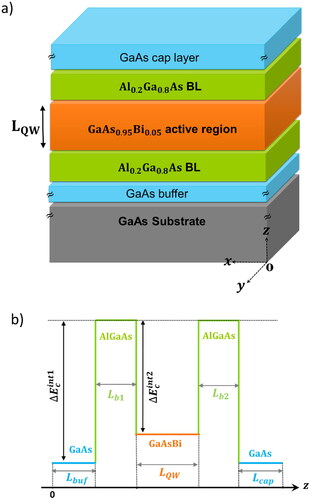
Hence, the analytical expression for within each semiconductor constituting the overall structure is:
(7)
(7)
serves as a summary of the abbreviations used to refer to the various layer thicknesses in EquationEq. (7)(7)
(7) . The magnitudes of the confinement potential depths, denoted as
and
in EquationEq. (7)
(7)
(7) , encapsulating the interface separation between the GaAs and its adjoining barrier layers, and the barrier and QW layer, respectively, were garnered from Massoudi (Citation2019). We set the width of the barrier layer at
while adjusting other parameters for specific objectives in this study. The determination of the intersubband bottom energies, confinement potential profile, and their associated wave functions is achieved through the solution of EquationEqs. (1–7).
Table 2. Summary of the used abbreviations.
2.3. Intersubband optical absorption coefficient
The rate of transition from the initial to the final subbands and
triggered by a wave
with a frequency
and amplitude
and, is determined by the Fermi golden rule (Zhang & Liu, Citation2016). The intersubband absorption coefficient
can be calculated as the energy loss per unit volume per unit time, divided by the intensity of the incident light (Gil, Citation2017). Hence, the optical absorption coefficient (AC) for the ISBT in GaAsBi/AlGaAs SQW structures can be computed as follows:
(8)
(8)
represents the active volume,
denotes the active layer refractive index,
is the vacuum speed of light, and
stands for the vacuum permittivity. The terms
(initial state energy) and
(final state energy) are involved in the summation, which encompasses all conceivable initial and final states. The Fermi-Dirac distribution
known as the probability function, provides the likelihood that an electron will occupy a quantum state at the energy level
When considering the absorption between the two successive subbands
and
the summation can be described as the disparity separating two subband populations:
(9)
(9)
Hence, the formula for the optical AC between subbands and
can be expressed as:
(10)
(10)
In this context, the carrier surface density in the respective subband is denoted as
is the dipole matrix element and
represents the crystal surface.
3. Results and discussion
, b, and c show the confinement potential of the CB profile for the three studied structures A (), B (
), and C (
), respectively, with (continuous red curve) and without (dotted black line) including the effect of doping on the active region, along the
-direction. Other parameters are uniform across all structures, including the intersubband relaxation time (
Albuquerque, Fulco, Vasconcelos, & Mauriz, Citation2013; Marko et al., Citation2016). The selected widths are tailored to induce variations in the ISBT energy within the terahertz frequency domain. A curved profile (GaAsBi) is observed in the center of the well, indicating that the bottom of the CB is greatly modified under doping. Furthermore, the electrostatic potential in the BL regions (AlGaAs) declined with systematic sharpness. Therefore, in n-doped GaAsBi/AlGaAs quantum wells, increasing the well width reshapes the CB structure. To explain this behaviour, we summarize in the results of the calculations of the Fermi level and the various subband energy levels in the GaAsBi/AlGaAs QW in terms of the active layer thickness, taking into consideration the impact of doping on the active region and applying a donor density of
Figure 2. The conduction band profiles for the studied structures A (a), B (b), and (c) along the - direction. The left contact on the CB was set to zero energy arbitrarily.
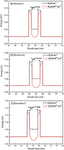
Figure 3. Energy level diagram of GaAsBi/AlGaAs SQW for the three studied structures A, B, and C. ISBT for structure a is ISBT1A, for structure B are respectively ISBT1B, ISBT2B, and for structure C are respectively ISBT1C, ISBT2C, SBT3C.
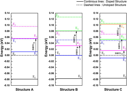
Indeed, in n-doped quantum wells, the neutrality equation remains fundamental to governing charge carrier equilibrium, due to the increased carrier density, the Fermi level adjusts upward to maintain equilibrium. Furthermore, by expanding the width, the quantum well becomes deeper, enhancing electron confinement. Quantum confinement effects result in a compression of energy levels within the quantum well, providing more available states for charge carriers, including intrinsic and donor electrons. This is proved in , where the doping creates a new energy level in the quantum well of structure C, compared to the same undoped structure. Furthermore, the redistribution of charge carriers towards higher energy levels near the conduction band edge contributes to the overall elevation of the Fermi level from
to
as
grows from
to
Consequently, redshifts are caused by the synergetic effect of doping and increased quantum well width in all states due to the decrease in bottom conduction band values. These results highlight the significant impact of doping and well thickness on ISBT in GaAsBi/AlGaAs heterostructures (Ajay et al., Citation2017; Chand, Citation1993).
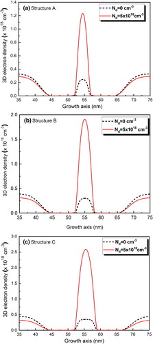
–c show the three-dimensional electron density profiles for the three studied structures by considering the doping effect as a function of position along the growth axis (continuous red curves). The undoped active layer density is also added for comparison (dashed curves). The figure shows that for all structures, doping parameters did not alter the density shape, but greatly increased its magnitude. Moreover, increasing the QW width yields the highest electron density. For example, in structure C, doping increases the 3D-electron density in the QW center from
to
Meanwhile, the electron density calculated under doping in Structure A represents
of that observed in Structure C. As a result, the combined effects of increasing the quantum well (QW) width and introducing doping have a direct impact on the concentration of negative charge carriers, leading to an overall increase in density.
Figure 4. The 3D electron density for structures A (a), B (b), and (c).
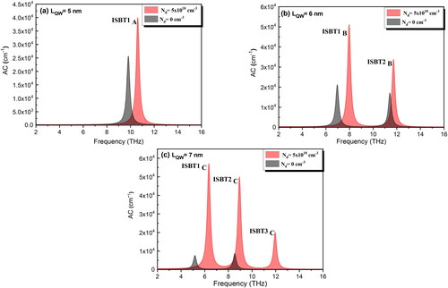
To gain deeper insights and optimize the doping concentration of the active layer for terahertz applications, we show in –c the absorption coefficient (AC) calculated according to EquationEq. (10)(10)
(10) in terms of the incident frequency for the three studied heterostructures A, B, and C, respectively. Each AC peak corresponds to an ISBT as revealed in . The initial observation reveals a clear influence of doping parameters on both the absorption intensity and position. In structure A, there is a single peak, in structure B, there are two peaks, and in structure C, there are three peaks. The results indicate that increasing well width introduces additional ISBTs and amplifies the effect of doping on AC. Furthermore, doping shifts the transition frequencies slightly, affecting subband energy levels.
Figure 5. The absorption coefficient AC for structures A (a), B (b), and C (c) for doped and undoped GaAsBi/AlGaAs heterostructures.
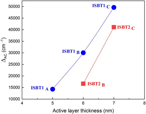
To highlight this behaviour, we plot in the variation in the intensity difference of the absorption coefficient between doped and undoped structures for the GaAsBi active layer thickness. Remarkably, the impact of doping becomes increasingly pronounced with the augmentation of the active layer width. For instance, elevating the doping concentration from
to
results in an increase in the photon AC intensity within structure C. Specifically, the AC intensity for ISBT1C rises from
to
In the same structure under the influence of doping, the AC peak associated with the first intersubband transition (ISBT1C) is observed at a frequency of
Figure 6. The variation in the intensity difference of the absorption coefficient, between doped and undoped structures for the GaAsBi active layer thickness.
In contrast, for structure A with an of
the same transition occurs at
This shift towards lower energy values, indicative of a redshift, is primarily attributed to the modulation of the confinement potential profile achieved by altering the GaAsBi active layer thickness. Indeed, the widening of the doped layer leads to increasing Hartree potential and consequently, a deepening of the QW. This, in turn, results in the introduction of novel states and a decline in the separation of pre-existing confined states, this is particularly prominent when doping is introduced. The manifestation of this behaviour is evident in . Rodríguez-Magdaleno, Turkoglu, Ungan, Mora-Ramos, and Martínez-Orozco (Citation2021) interpreted this through the examination of the Fermi occupation function and the dipole matrix element. The swift rise in the dipole matrix element with the active layer thickness signifies an expanded overlap between the ground and first wavefunctions (Massoudi, Citation2019).
provides a comprehensive 3D analysis of the absorption coefficient (AC) in GaAsBi/AlGaAs quantum wells, illustrating its variation with frequency alongside two key parameters: active layer thickness and doping concentration. shows the AC's dependence on frequency and active layer thickness at a fixed doping concentration of The results reveal that as the active layer thickness increases, the peak absorption frequencies shift significantly. This shift indicates enhanced confinement of charge carriers, which modifies the energy levels within the quantum well. Since, the first ISBT emerges as a critical aspect in these plots, presenting the most significant transition structures due to the high overlap of wavefunctions between the lowest energy states. Indeed, in a quantum well, this transition is the most prominent due to reduced scattering and non-radiative recombination processes while higher energy states are more likely to interact with phonons and other carriers (Cavill, Hawker, & Kent, Citation2003; Langer et al., Citation2014). The data in highlight an optimal thickness range around
where the AC reaches its maximum at
for the ISBT1C. Moreover, our analysis confirms that a quantum well width of 7 nm is optimal, as it provides the desired AC within the desired terahertz domain extending from
to
illustrates the AC variation with frequency and doping concentration at a fixed quantum well width of
A scan of the absorption coefficient over a concentration range from
to
for the structure with
shows that the AC of the first ISBT increases rapidly with doping concentrations until it reaches a plateau starting at around
where it remains almost unchanged. Contrewhise to the second and third ISBTs, they show a continuous AC intensity increase. This behaviour is due to the elevated carrier density and resulting modifications in the electronic structure (Yanagi et al., Citation2018).
Figure 7. (a) 3D plot showing the variation of the absorption coefficient (AC) with frequency and active layer thickness at a fixed doping concentration (). (b) 3D plot depicting the variation of the AC with frequency and active layer doping concentration at a fixed quantum well width (
).
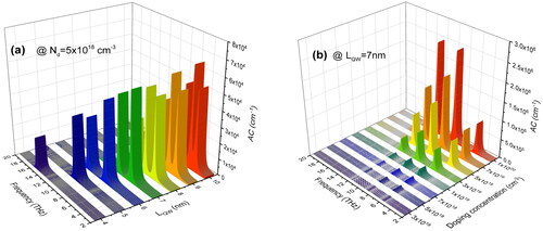
Figure 8. Structure C absorption coefficient at different doping levels of GaAsBi quantum well.
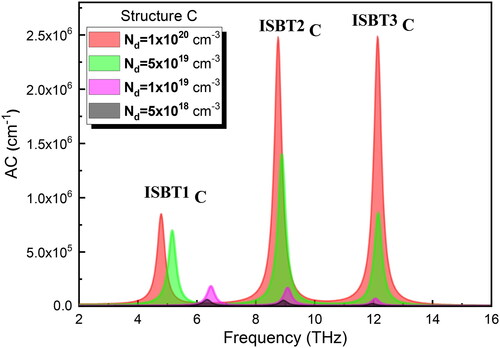
To create a more detailed image on the effect of doping on the THz frequency characteristics of the examined structure ( structure C) for the second and the third ISBTs, we display in the absorption coefficient calculated for four distinct values of ionized impurity densities (
With increasing the value of the concentration
the AC intensity increases considerably. For example, for the second intersubband transition (ISBT2C) AC increases from
to
Indeed, the elevated doping concentration results in a deeper confinement potential. As a result, the confined states converge, and the higher energy levels become closer together. Due to the closer proximity of energy levels, the absorption coefficient for the third intersubband transition (ISBT3C) decreases. Accordingly, the concentration of the doping layer can be adjusted to get the desired absorption coefficient. Furthermore, doping also alters the AC peak position and higher doping lowers the THz frequency value of absorption; an increase in doping from
to
results in a redshift in the ISBT2C absorption peak position from
to
THz. The observed influence of doping concentration on the THz optical properties opens up promising avenues for the design of THz optical devices such as filters or modulators, where the doping concentration serves as a parameter to fine-tune the device’s performance, with precise control over their characteristics.
4. Conclusion
In summary, the investigation focused on the combined influence of doping and active layer thickness in GaAsBi/AlGaAs quantum wells on the absorption coefficient. This was achieved by coupling Schrödinger and Poisson equations in the SC approach. By expanding the doped layer width, a deeper quantum well confinement is produced. This leads to an elevation in both electron density and electrostatic potential and a redshift, accompanied by a higher absorption peak intensity. Furthermore, various doping profiles have been examined to understand how they affect GaAsBi/AlGaAs SQW optical operation. The findings highlight a significant increase in the intensity of the AC peak, spanning several orders of magnitude, with increasing the value of the doping concentration. This is associated with a shift toward the lower THz frequency depending on the ISBT in the related peak energy. The obtained results can open up avenues for developing tailored and tunable THz technologies with applications spanning communication, imaging, and sensing.
Author’s Contributions
The study was done by Dr. Amani Rached.
Acknowledgments
The author acknowledges the support of the Basic and Applied Scientific Research Center at Imam Abdulrahman Bin Faisal University.
Disclosure statement
The authors declare no competing interests.
Data availability
All results exist in the main manuscript.
References
- Adachi, S. (1985). GaAs, AlAs, and AlxGa1 − xAs: Material parameters for use in research and device applications. Journal of Applied Physics, 58(3), R1–R29. doi:10.1063/1.336070
- Ajay, A., Lim, C. B., Browne, D. A., Polaczyński, J., Bellet-Amalric, E., Bleuse, J., … Monroy, E. (2017). Effect of doping on the intersubband absorption in Si- and Ge-doped GaN/AlN heterostructures. Nanotechnology, 28(40), 405204. doi:10.1088/1361-6528/aa8504
- Alazmi, B. O., Althebyani, H. H. H., Zaied, I., Fitouri, H., & Rebey, A. (2023). Thermal annealing effects on the physical properties of GaAsBi/GaAs/GaAs:Si structure. Journal of Umm Al-Qura University for Applied Sciences 9(2), 164–175. doi:10.1007/s43994-022-00023-4
- Albuquerque, E. L., Fulco, U. L., Vasconcelos, M. S., & Mauriz, P. W. (2013). Optical gain spectra of unstrained graded GaAs/AlxGa1 − xAs quantum well laser. Physics Letters A, 377(7), 582–586. doi:10.1016/j.physleta.2012.12.025
- Amenabar, I., Poly, S., Nuansing, W., Hubrich, E. H., Govyadinov, A. A., Huth, F., … Hillenbrand, R. (2013). Structural analysis and mapping of individual protein complexes by infrared nanospectroscopy. Nature Communications, 4(1), 2890. doi:10.1038/ncomms3890
- Beeler, M., Bougerol, C., Bellet-Amalaric, E., & Monroy, E. (2014). THz intersubband transitions in AlGaN/GaN multi-quantum-wells. Physica Status Solidi (a), 211(4), 761–764. doi:10.1002/pssa.201300431
- Ben Nasr, A., Habchi, M. M., Bilel, C., Rebey, A., & El Jani, B. (2015). Carriers confinement study of GaNAsBi/GaAs QWs emitting at 1.3 and 1.55 μm. Semiconductors, 49(5), 593–599. doi:10.1134/S1063782615050048/METRICS
- Bhouri, A., Rached, A., & Lazzari, J. L. (2015). Resonant tunneling transport in AlzGa1 − zN/InxGa1 − xN/AlzGa1 − zN/InyGa1 − yN quantum structures. Journal of Physics D: Applied Physics, 48(38), 385102. doi:10.1088/0022-3727/48/38/385102
- Busby, Y., Capellini, G., Evangelisti, F., Rtolani, M. O., Virgilio, M., Grosso, G., … De Seta, M. (2010). Terahertz intersubband transitions in the conduction band of Ge/SiGe multi quantum wells. In IRMMW-THz 2010 - 35th International Conference on Infrared, Millimeter, and Terahertz Waves, Conference Guide. doi:10.1109/ICIMW.2010.5612749
- Cavill, S. A., Hawker, P., & Kent, A. J. (2003). Carrier–phonon interactions in semiconductor quantum dots and wires. In L. J. Challis (Ed.), Electron-phonon interactions in low-dimensional structures (pp. 115–148). Oxford University Press. doi:10.1093/ACPROF:OSO/9780198507321.003.0004
- Chand, N. (1993). Growth of high quality AlGaAs/GaAs heterostructures by molecular beam epitaxy for photonic and electronic device applications. Thin Solid Films, 231(1–2), 143–157. doi:10.1016/0040-6090(93)90709-X
- Donmez, O., Aydın, M., Ardalı, Ş., Yıldırım, S., Tıraş, E., Nutku, F., … Erol, A. (2020). Electronic transport in n-type modulation-doped AlGaAs/GaAsBi quantum well structures: Influence of Bi and thermal annealing on electron effective mass and electron mobility. Semiconductor Science and Technology, 35(2), 025009. doi:10.1088/1361-6641/ab5d8d
- Donmez, O., Aydın, M., Mutlu, S., Puustinen, J., Hilska, J., Guina, M., & Erol, A. (2023). Comprehensively analysis of hot electron transport in as-grown and thermally annealed n-type modulation-doped Al0.15Ga0.85As/GaAs0.96Bi0.4 quantum well structure. Materials Science in Semiconductor Processing, 154, 107227. doi:10.1016/j.mssp.2022.107227
- Donmez, O., Erol, A., Çetinkaya, Ç., Çokduygulular, E., Aydın, M., Yıldırım, S., … Guina, M. (2021). A quantitative analysis of electronic transport in n- and p-type modulation-doped GaAsBi/AlGaAs quantum well structures. Semiconductor Science and Technology, 36(11), 115017. doi:10.1088/1361-6641/ac2af0
- Eisele, M., Cocker, T. L., Huber, M. A., Plankl, M., Viti, L., Ercolani, D., … Huber, R. (2014). Ultrafast multi-terahertz nano-spectroscopy with sub-cycle temporal resolution. Nature Photonics, 8(11), 841–845. doi:10.1038/nphoton.2014.225
- Ergün, S., & Sönmez, S. (2015). Terahertz technology for military applications. Journal of Military and Information Science, 3(1), 13–16. doi:10.17858/jmisci.58124
- European Commission’s work programme for the Technical Support Instrument under Regulation (EU) 2021/240 of the European Parliament and of the Council. (2023).
- Fernandes Pereira, M., & Apostolakis, A. (n.d). Terahertz (THz), Mid Infrared (MIR) and Near Infrared (NIR) Technologies for Protection of Critical Infrastructures Against Explosives and CBRN, http://www.nato.int/science.
- Gil, B. (2017). Oxford Scholarship Online Devices, 1–36.
- Horiuchi, N. (2019). Room-temperature terahertz detector. Nature Photonics, 13(9), 584–584. doi:10.1038/s41566-019-0513-4
- Krotkus, A., Nevinskas, I., Norkus, R., Geižutis, A., Strazdienė, V., Pačebutas, V., & Paulauskas, T. (2023). Terahertz photocurrent spectrum analysis of AlGaAs/GaAs/GaAsBi multi-junction solar cells. Journal of Physics D: Applied Physics, 56(35), 355109. doi:10.1088/1361-6463/acd85d
- Langer, T., Pietscher, H. G., Ketzer, F. A., Jönen, H., Bremers, H., Rossow, U., … Hangleiter, A. (2014). S shape in polar GaInN/GaN quantum wells: Piezoelectric-field-induced blue shift driven by onset of nonradiative recombination. Physical Review B, 90(20), 205302. doi:10.1103/PHYSREVB.90.205302/FIGURES/8/MEDIUM
- Latthiwan, P., Sikam, P., Moontragoon, P., Klinkla, R., Watcharapasorn, A., Hussain, T., & Kaewmaraya, T. (2024). Controllable terahertz intersubband absorptions in ZnO/(Sb,N) co-doped ZnO quantum wells: First-principles study. Journal of Physics and Chemistry of Solids, 185, 111765. doi:10.1016/j.jpcs.2023.111765
- Lewis, R. A. (2019). A review of terahertz detectors. Journal of Physics D: Applied Physics, 52(43), 433001. doi:10.1088/1361-6463/ab31d5
- Liu, N., Dan, M., Hu, G., & Zhang, Y. (2022). Piezo-phototronic intersubband terahertz devices based on layer-dependent van der Waals quantum well. Nano Energy, 94, 106912. doi:10.1016/j.nanoen.2021.106912
- Marko, I. P., Broderick, C. A., Jin, S., Ludewig, P., Stolz, W., Volz, K., … Sweeney, S. J. (2016). Optical gain in GaAsBi/GaAs quantum well diode lasers. Scientific Reports, 6(1), 28863. doi:10.1038/srep28863
- Marko, I. P., Jin, S. R., Hild, K., Batool, Z., Bushell, Z. L., Ludewig, P., … Sweeney, S. J. (2015). Properties of hybrid MOVPE/MBE grown GaAsBi/GaAs based near-infrared emitting quantum well lasers. Semiconductor Science and Technology, 30(9), 094008. doi:10.1088/0268-1242/30/9/094008
- Marko, I. P., Ludewig, P., Bushell, Z. L., Jin, S. R., Hild, K., Batool, Z., … Sweeney, S. J. (2014). Physical properties and optimization of GaBiAs/(Al)GaAs based near-infrared laser diodes grown by MOVPE with up to 4.4% Bi. Journal of Physics D: Applied Physics, 47(34), 345103. doi:10.1088/0022-3727/47/34/345103
- Maspero, R., Sweeney, S. J., & Florescu, M. (2016). Unfolding the band structure of GaAsBi. Journal of Physics. Condensed Matter: An Institute of Physics Journal, 29(7), 075001. doi:10.1088/1361-648X/aa50d7
- Massoudi, I. (2019). Terahertz intersubband transitions in GaAsBi/AlGaAs single quantum well heterostructure. Superlattices and Microstructures, 136, 106299. doi:10.1016/j.spmi.2019.106299
- NATO - Topic: Integrated Air and Missile Defence (NATO IAMD). (2024) https://www.nato.int/cps/en/natohq/topics_8206.htm.
- NSM Archive - Physical Properties of Semiconductors. (2024) http://www.matprop.ru/.
- Office of the Under Secretary of Defense, Department of Defense Fiscal Year (FY) 2024 Budget Estimates. (2023).
- Pač̌ebutas, V., Bertulis, K., Aleksejenko, G., & Krotkus, A. (2009). Molecular-beam-epitaxy grown GaBiAs for terahertz optoelectronic applications. Journal of Materials Science: Materials in Electronics, 20, 363–366. doi:10.1007/S10854-008-9625-1/METRICS
- Pačebutas, V., Butkutė, R., Čechavičius, B., Stanionytė, S., Pozingytė, E., Skapas, M., … Krotkus, A. (2017). Bismides: 2D structures and quantum dots. Journal of Physics D: Applied Physics, 50(36), 364002. doi:10.1088/1361-6463/aa7bdb
- Pačebutas, V., Stanionytė, S., Arlauskas, A., Norkus, R., Butkutė, R., Geižutis, A., … Krotkus, A. (2018). Terahertz excitation spectra of GaAsBi alloys. Journal of Physics D: Applied Physics, 51(47), 474001. doi:10.1088/1361-6463/aadb11
- Pettinari, G., Drachenko, O., Lewis, R. B., & Tiedje, T. (2016). Electron effective mass enhancement in Ga(AsBi) alloys probed by cyclotron resonance spectroscopy. Physical Review B, 94(23), 235204. doi:10.1103/PHYSREVB.94.235204/FIGURES/3/MEDIUM
- Pūkienė, S., Karaliūnas, M., Jasinskas, A., Dudutienė, E., Čechavičius, B., Devenson, J., … Valušis, G. (2019). Enhancement of photoluminescence of GaAsBi quantum wells by parabolic design of AlGaAs barriers. Nanotechnology, 30(45), 455001. doi:10.1088/1361-6528/ab36f3
- Rached, A., Bhouri, A., Sakr, S., Lazzari, J. L., & Belmabrouk, H. (2016). Self-consistent vertical transport calculations in AlxGa1–xN/GaN based resonant tunneling diode. Superlattices and Microstructures, 91, 37–50. doi:10.1016/j.spmi.2015.12.035
- Rebey, A., Mbarki, M., Rebei, H., & Messaoudi, S. (2022). Performance optimization of AlGaAs/GaAsBiN resonant tunneling diode. Optik (Stuttg), 268, 169793. doi:10.1016/j.ijleo.2022.169793
- Rodríguez-Magdaleno, K. A., Turkoglu, A., Ungan, F., Mora-Ramos, M. E., & Martínez-Orozco, J. C. (2021). Donor impurity atom effect on the inter-subband absorption coefficient for symmetric double n-type δ-doped GaAs quantum well. Superlattices and Microstructures, 156(2021), 106988. doi:10.1016/j.spmi.2021.106988
- Simmons, R. A., Jin, S. R., Sweeney, S. J., & Clowes, S. K. (2015). Enhancement of Rashba interaction in GaAs/AlGaAs quantum wells due to the incorporation of bismuth. Applied Physics Letters, 107(14), 142401. doi:10.1063/1.4932122/29623
- Terahertz Technology in Defense: Enhancing Military Capabilities. (n.d). https://ts2.space/en/terahertz-technology-in-defense-enhancing-military-capabilities/#gsc.tab=0.
- Usman, M., Broderick, C. A., Lindsay, A., & O’Reilly, E. P. (2011). Tight-binding analysis of the electronic structure of dilute bismide alloys of GaP and GaAs. Physical Review B, 84(24), 245202. doi:10.1103/PHYSREVB.84.245202/FIGURES/13/MEDIUM
- Vurgaftman, I., Meyer, J. R., & Ram-Mohan, L. R. (2001). Band parameters for III–V compound semiconductors and their alloys. Journal of Applied Physics, 89(11), 5815–5875. doi:10.1063/1.1368156
- Yanagi, K., Okada, R., Ichinose, Y., Yomogida, Y., Katsutani, F., Gao, W., & Kono, J. (2018). Intersubband plasmons in the quantum limit in gated and aligned carbon nanotubes. Nature Communications, 9(1), 1121. doi:10.1038/s41467-018-03381-y
- Yu, L., Li, D., Zhao, S., Li, G., & Yang, K. (2012). First principles study on electronic structure and optical properties of ternary GaAs:Bi alloy. Materials, 5(12), 2486–2497. doi:10.3390/ma5122486
- Zayan, A., Stevens, M., & Vandervelde, T. E. (2016). GaAsBi alloys for photovoltaic and thermophotovoltaic applications. In 2016 IEEE 43rd Photovoltaic Specialists Conference (PVSC) (pp. 2839–2843), doi:10.1109/PVSC.2016.7750172
- Zhang, J., Fai Mak, K., Nagl, N., Seidel, M., Bauer, D., Sutter, D., … Pronin, O. (2018). Multi-mW, few-cycle mid-infrared continuum spanning from 500 to 2250 cm−1. Light, Science & Applications, 7, 17180–17180. doi:10.1038/lsa.2017.180
- Zhang, J. M., & Liu, Y. (2016). Fermi’s golden rule: Its derivation and breakdown by an ideal model. European Journal of Physics, 37(6), 065406. doi:10.1088/0143-0807/37/6/065406