
Abstract
Aniline is a mutagenic and carcinogenic material for human health, and it is desirable to construct high-performance detecting system for the trace detection of aniline. In this work, the boron (B)/nitrogen (N)-doped diamond (BND) films prepared by chemical vapor deposition are proposed as electrochemical electrodes to detect aniline in a wide concentration scale. The BND electrodes have a high sensitivity (detect limitation of 0.29 μmol L−1) and a wide linear detection range (0.5 − 500 μmol L−1). Both the detection limitation and linear range are significantly improved with respect to that from traditional electrodes of boron-doped diamond and various carbonaceous materials, which can be attributed to the synergistic effect of increased electrochemistry reduction and density of reaction sites on the BND electrode surfaces. This work develops a kind of electrochemical electrodes of B/N-doped diamond films with high performances for quantitative detections of aniline in practical applications.
Supplemental data for this article is available online at http://dx.doi.org/10.1080/26941112.2021.1939170
1. Introduction
Aniline is an important industrial raw material widely used in wild application fields, such as printing and dyeing, dyes, rubber, pharmaceuticals, explosives, and pesticides [Citation1,Citation2]. It is accepted that aniline could cause damage to central nervous systems through the skin absorption, respiratory tract, and digestive tract [Citation3]. It is essential and desirable to detect the traces of aniline [Citation4]. Up to now, various techniques have been developed to detect aniline, such as surface-enhanced Raman scattering (SERS) [Citation5], electrochemiluminescence (ECL) [Citation6], liquid chromatography [Citation7,Citation8], gas chromatography [Citation9], and electrochemistry methods [Citation10–12]. The corresponding results in the previous literature are summarized in . For the optical methods, the reported detection limits of the optical testing methods are as low as 10−4 to 10−3 µmol L−1 [Citation5,Citation6], and the linear detection ranges of these developed techniques are relatively narrow in the region of 0.001 − 10 μmol L−1. However, the Raman scattering technique requires lasers with resonant wavelengths to realize SERS signals [Citation5], and its optical system is easily affected by the ambient atmosphere. A preconcentration process is generally required in the Raman technique to improve the test sensitivity [Citation5,Citation13–15]. The ECL method [Citation6] exhibits good reproducibility and stability. However, a large amount of expensive reagents are consumed during ECL examinations, and the byproducts could cause environmental pollutions [Citation16]. The necessary processes of preconcentration, purge and trap, solid-phase extraction, and liquid-liquid extraction make the liquid and gas chromatography methods complex and time-consuming [Citation17,Citation18].
Table 1. The detection limit and linear range of aniline detection by various methods.
In recent years, electrochemistry methods have been performed for trace detection of numerous pollutants [Citation18–20] because of their advantages of easy operation, high sensitivity and selectivity, low reagent consumption, wide dynamic range, low detection limit, and low cost, being superior to the optical testing methods. Several kinds of electrochemical sensors were reported to detect aniline using electrodes of screen-printed carbon [Citation10], nanoporous gold (NP-Au) [Citation11], and boron-doped diamond (BDD) film [Citation12]. However, there are some obstacles in the present electrochemistry methods to be overcome. As listed in , the detection limits (linear scales) are relatively high (narrow) for the electrodes of screen-printed carbon or NP-Au films. Notably, during the detection processes, the surfaces of these conventional electrode materials would absorb numerous polymerization reaction products, and the corresponding active sites would block electrochemical reactions, leading to deactivations of the electrodes and lower sensitivities [Citation10,Citation11].
BDD has been widely utilized in electroanalyses, electrocatalyses, and electrochemical sensors [Citation17–23]. The conductive diamond electrodes have unique advantages of low background current, wide electrochemical potential window, low adsorption property, stable physical and chemical properties. The material is suitable for high-performance electrochemical detections [Citation22,Citation24–28]. In Ref. [Citation12], BDD electrode-based electrochemical sensor was firstly proposed to detect aniline. Although BDD has intrinsic advantages as electrodes, neither the reported detection limit nor linear range showed significant improvements over the other kinds of electrodes [Citation10,Citation11].
B/N co-doped diamond (BND) has been considered as a novel electrode rather than BDD, due to its synergistic effect of introducing catalyst active sites and promoting redox reaction [Citation21,Citation29,Citation30]. The doping N and B atoms in diamond will reduce charge-transfer resistance and increase electrochemical potential window [Citation30,Citation31]. In this work, the performances of BND electrodes are examined to detect aniline. The detection limit and linear range are successfully improved over BDD electrodes. Furthermore, the properties of stability, reproducibility, and usability of the BND-based sensors are tested for aniline detections.
2. Materials and methods
The reagents used in the experiments were all of the analytical grade. A 0.1 mol L−1 phosphate buffer solution (PBS, pH = 2.0) was used as a solvent to dilute the compounds in the experimental procedures. The polycrystalline BND and BDD films were fabricated by microwave plasma chemical vapor deposition (MPCVD) technique on p-type silicon substrates with an area size of ∼4.6 × 4.8 mm2. The substrate temperature was monitored by an optical pyrometer and set as ∼850 °C. The BND films were fabricated with CH4/H2/B/N2 flow rate of 2/200/2/2 sccm under a total pressure of 7 kPa. Liquid B(OCH3)3 was employed as the incorporated boron source at 25 °C, carried by H2 gas. The BND films were deposited for 8 h. The BDD films were fabricated under the same conditions of the BND films without introducing nitrogen gas.
The morphologies, crystal properties, surface bonds, and surface chemical states of the films were characterized by scanning electron microscopy (SEM, JSM-6480LV), X-ray diffraction (XRD, RigakuD/MAX-RA), Raman spectroscopy (Renishaw in via Raman microscope equipped with 532 nm laser excitation), and X-ray photoelectron spectroscopy (XPS, VG ESCALAB MK II), respectively.
The room temperature electrochemical measurements were performed on an Electrochemical Workstation (CHI 760E) three-electrode system. An appropriate amount of aniline with 0.1 mol L−1 PBS (pH = 2.0) was diluted as standard solutions. The 0.5 − 500 μmol L−1 aniline standard solutions were poured into the electrochemical cell of the three-electrode system. The conductive BND and BDD films were used as the working electrodes. A platinum wire was employed as the counter electrode, and a saturated calomel was the reference electrode.
3. Results and discussion
3.1. Morphology and structure of BND and BDD films
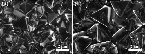
As shown in , the as-grown polycrystalline BND films consist of dense grains with sizes in the scale of about 1 − 2 μm. The average grain size of the BDD films is slightly larger than that of the BND films (). The BND and BDD films mainly consist of (111)-orientated grains with clear boundaries and smooth surface, indicating the high quality of the films. The thicknesses of the BDD and BND electrodes are about 9 μm and 10 μm, respectively, observed from the corresponding cross-sectional SEM images (Figure S1).
Figure 1. SEM images of BND (a) and BDD (b) films.
shows the Raman spectrum of the BND film, as well as the BDD film. For the BDD sample, the typical asymmetric diamond peak of 1332 cm−1 was observed with the broad peak centered at 500 cm−1 and 1200 cm−1, attributed to the Fano effect and density of states (DOS) by heavy boron doping, similar to the reported data of BDD samples [Citation19,Citation32–34].
Figure 2. (a) Raman spectra and (b) XRD patterns of BND and BDD films.
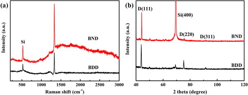
shows the Raman spectra obtained from the (111) facets of grains in the samples synthesized at high B-doping levels. In general, the intensities and frequencies of the diamond zone-center photo band and DOS-related bands change with varying B-doping levels.
Noted that for the BND sample, additionally, the broad bands of 1500 cm−1 indicate that the non-diamond carbon mainly comes from the grain boundaries, while the stronger 1500 cm−1 band of the BND film is due to nitrogen atoms preferentially entering the grain boundaries and promoting the formation of sp2 C-N bonds [Citation35,Citation36]. The broad bands of 2060 cm−1 of the BND film corresponds to N-V0 formed by the recombination of nitrogen and vacancies [Citation37]. The broad bands in a wide region of 1500–3000 cm−1 from BND are distinguished from the BDD sample. Besides the contribution of increased sp2 carbon, the bands would be related to the additional phonon vibrations from co-doped B and N that induce various phonon density of states of diamond. The background of the photoluminescence from the N-V0 centers with phonon replica is included in this region. The Raman measurement indicates that high quality BND films have been achieved here.
shows the XRD patterns of the BND and BDD films. The diffraction peaks at 44.1°, 75.5°, and 91.8° correspond to the (111), (220), and (311) planes of diamond, respectively [Citation17,Citation35,Citation36]. The dominant (111) and (220) peaks denote that the BND and BDD films mainly consist of (111) and (110) orientated grains, which is accordant with the SEM images shown in .
XPS measurements were performed to determine the state of N and B dopants in the BND film. is an XPS spectrum of the BND, showing two fitted peaks at 185.8 eV and 190.8 eV, attributed to B-C and B-N, respectively. shows the B-C bond peak (190.1 eV) of the BDD electrode. Comparing to the B-C bond peak (185.8 eV) of the BND, the shift to a lower binding energy is attributed to the formation of B-N bonds in the BND electrode. Two fitted peaks at 398.6 eV and 399.3 eV are observed in the N 1 s spectrum of the BND electrode (), being assigned to N-B and N-C, respectively. indicates no evident peaks of N 1 s from the BDD sample, which means that the surface absorption of nitrogen in air on the diamond surface could be ignored. The noticeable N 1 s spectrum of the BND electrode confirmed the successful boron and nitrogen incorporation in diamond.
Figure 3. XPS spectra of the BND and BDD electrodes. (a) B 1 s, (c) N 1 s, and (e) C 1 s of the BND electrode: (b) B 1 s, (d) N 1 s, and (f) C 1 s of the BDD electrode.
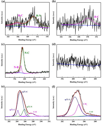
shows the C 1 s apectrum of the BND electrode. There are four fitted peaks at 284.2 eV, 284.8 eV, 285.9 eV, and 287.5 eV, attributed to sp2 C-C, sp3 C-C, sp2 C-N, and C-O, respectively. In the C 1 s spectrum of the BDD electrode (), two fitted peaks at 284.3 eV and 286.9 eV could be assigned to the sp3 C-C and C-O, respectively. The peak at 285.1 eV is attributed to sp3 C-C surface group of the hydrogen-terminated diamond. Furthermore, the XPS spectra indicated that the BND electrode reveals a substantially higher sp2 species than the BDD electrode (about 21.4%), similar to the literate [Citation19,Citation31,Citation38].
3.2. Electrochemical characterization for aniline detections
shows the cyclic voltammograms (CVs) of the BND and BDD electrodes in an aniline solution with a concentration of 100 μmol L−1 (scanning rate: 0.3 V s−1).
Figure 4. CVs on the BND electrode (red line) and BDD electrode (black line) in pH 2.0 buffer solution containing 100 μmol L−1 aniline. The scan rate is 0.3 V s−1.
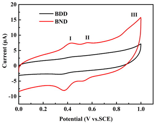
Two reduction peaks are evidenced in the CV curve of the BND electrode, with peak potentials of ca. 0.37 V and 0.53 V. Two redox couples were identified from the presence of two pairs of reversible peaks, labeled as I and II, respectively, in . It indicates that the BND electrode is more sensitive to detect aniline for a higher reduction peak I (-8.06 μA) than that of the BDD electrode (-2.71 μA). The reduction peak II current of the BND electrode is -4.92 μA, while no apparent peak current appears with the BDD electrode. An oxidation peak potential is observed at 0.95 V, labeled as III in . According to the aniline oxidation mechanism in literature [Citation39, Citation40], the widely accepted mechanism of the entire oxidation reaction is also applicable to the BND electrode, including the formation of nitrene cations of aniline in the range of the peak III. It is responsible for the occurrence of reversible redox peaks I and II that nitrene cations give rise to the dimeric products p-aminodiphenylamine and benzidine by rapid follow-up reactions [Citation12]. The peak III is not suitable for analytical applications of aniline content because the entire anodic current derives from aniline oxidation and the oxidation of the dimeric species formed by coupling of nitrene cations [Citation12]. Different from aniline oxidation, the anodic oxidation of p-aminodiphenylamine and benzidine is electrochemically reversible processes.
In , the reduction peak current of the BND electrode is higher than that of the BDD electrode, which means that the BND electrode has more excellent ability in the detection of aniline. The introduction of N can improve the electrochemistry reduction performance of the electrode and improve the speed of reaction, give rise to the dimeric products p-aminodiphenylamine and benzidine [Citation21,Citation29,Citation41].
Meanwhile, B/N co-doping also makes the electrode hydrogen evolution potential more negative, more defects, lower charge-transfer resistance (Figure S2), more sensitiveness (Figure S3) and active sites [Citation27,Citation42]. Therefore, we use differential normal pulse voltammetry (DNPV) mode to detect aniline concentrations from the reduction peaks.
shows the miscellaneous CVs of 100 μmol L−1 aniline with different scan rates performed on the BND electrode. As the scan rate increases, the cathodic peak current increases linearly (Figure S4), indicating an adsorption-controlled process [Citation19]. The accumulation process could improve the sensitivity and decrease the detection limit. Through the control variable methods to explore suitable experimental conditions, it is found that the optimized accumulation potential is 0.95 V and accumulation time is 30 s (Figure S5 and S6).
Figure 5. (a) Five CVs of 100 μmol L−1 aniline on the BND electrode at different scan rates in 0.1 mol L−1 PBS (pH = 2.0). The scan rates are 0.1, 0.2, 0.3, 0.4 and 0.5 V s−1. (b) DNPV curves of 100 μmol L−1 aniline on the BND electrode in 0.1 mol L−1 PBS with pH value of 2.0, 4.0, 5.8, 7.0 and 8.0.
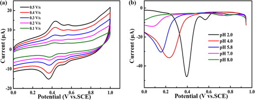
Generally, it is essential to investigate the effect of the pH on the DNPV response of aniline. shows the DNPV curves of the BND electrode measured at pH of 2.0 − 8.0 in PBS buffer solution with 100 μmol L−1 aniline. As the pH value increases, the potential of reduction peak shifts to lower potential, and the peak current decreases. The pH value of the buffer solutions is optimized at 2.0 in this work.
presents the DNPV diagrams of aniline solutions at different concentrations from 0.5 μmol L−1 to 500 μmol L−1 detected at the accumulation potential of 0.95 V for an accumulation time of 30 s. Obviously, the current intensity increases with the increase of the concentration of aniline, indicating that the peak current is sensitive to concentration of aniline. Meanwhile, there is no irreversible adsorption that leads to the passivation of the electrode in the detection of aniline. A noticeable reduction peak II current can be detected in the range of 10−4−10−7 mol L−1, while the peak current disappears when the concentration is higher than 10−4 mol L−1.
Figure 6. The DNPV diagrams of aniline with the different concentration from 0.5 μmol L−1 to 500 μmol L−1 on the BND electrode in 0.1 mol L−1 PBS (pH = 2.0) buffer solution.
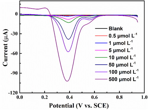
The detection range of the reduction peak II current is smaller than the peak I. Thus the reduction peak I current is better for aniline detection.
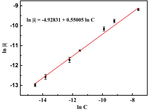
reveals the fitted linear relationship between the natural logarithm of the absolute value of peak I current and the natural logarithm of the concentration of aniline, and the correlation coefficient (R2) is 0.993. Based on the response of three times the standard deviation of zero-pose response, the detection limit is estimated to be 0.29 μmol L−1. The linear detection range (0.5–500 μmol L−1) of the BND electrode here is broader than other methods to detect aniline, such as BDD electrodes, screen-printed carbon electrodes, NP-Au films on glass substrates, and electrochemiluminescence quenching, as listed in . The broader range of quantitative detection is more conducive to the monitoring of aniline pollutants and environmental protection.
Figure 7. Calibration curve of aniline detections for BND electrode. The error bars represent the relative standard deviations of triple measurements.
The BND electrode is still active well after seven consecutive days of testing (Figure S7) meaning that the BND electrode-based sensor have excellent stability and repeatability. Additionally, the detection is rapid and straightforward. Thus BND is a promising electrode material for constructing high-performance electrochemical sensors to detect water pollution.
In order to test the potential for practical application of the BND sensor, further detection examination was completed in natural water samples that illustrate the practicality and universality of the sensor in various environments. The natural samples were collected from a lake at Jilin University. Compared with deionized water in laboratory, the collected natural water contained different ionic and other substances. The detection results of the natural water with different concentrations of aniline are summarized in . The sensor could detect aniline with a recovery rate of 97.0 − 108.2% and with relative standard deviations less than 5.4%. The results indicate that the BND sensor is suitable for detecting aniline in practical samples with high specificity and sensitivity.
Table 2. Recoveries of aniline with varying concentrations added in natural water samples.
4. Conclusions
In this work, we propose an efficient electrochemistry sensor based on BND electrodes to detect aniline. Examined by the DNPV method, a broad linear detection range of 0.5 − 500 μmol L−1 and a detection limit as low as 0.29 μmol L−1 are achieved, which are significantly improved with respect to the previous reports with various electrochemical electrodes. The BND-based sensors are of stability, reproducibility, and usability. These results in this work are helpful to construct novel diamond-based sensors to detect various substances with high sensitivity for environmental pollution detection and monitoring.
Supplemental Material
Download MS Word (713.2 KB)Disclosure statement
No potential conflict of interest was reported by the authors.
Additional information
Funding
Notes on contributors
Jiahan Li
Jiahan Li, master student in State Key Laboratory of Superhard Materials at Jilin University. His research topic on the applications of diamond thin films.
Qiliang Wang
Qiliang Wang, Senior Engineer of State Key Laboratory of Superhard Materials at Jilin University. His research focuses on the preparation and application of CVD diamond films.
Yaofeng Liu
Yaofeng Liu, PhD student in State Key Laboratory of Superhard Materials at Jilin University. His research topic is scanning electron microscope and Raman analysis.
Zhigang Jiang
Zhigang Jiang, Professor of State Key Laboratory of Superhard Materials at Jilin University. His research focuses on the preparation and application of CVD diamond films.
Junsong Liu
Junsong Liu, Associate Professor of State Key Laboratory of Superhard Materials at Jilin University. His research focuses on application of CVD diamond films.
Hongdong Li
Hongdong Li received the PhD degree in condensed matter physics from Jilin University, Changchun, China, in 1998. He is a PhD supervisor and group leader of the State Key Laboratory of Superhard Materials, Jilin University. His research interests include theoretical and experimental researches of diamond, wide bandgap semiconductor materials and optoelectronic devices.
Xiaoxi Yuan
Xiaoxi Yuan, Associate Professor of Institute for Interdisciplinary Quantum Information Technology at Jilin Engineering Normal University. Her research focuses on electrochemical sensors based on diamond.
References
- Grirrane A, Corma A, García H. Gold-catalyzed synthesis of aromatic azo compounds from anilines and nitroaromatics. Science. 2008;322(5908):1661–1664.
- Alagarsamy V, Raja Solomon V, Dhanabal K. Synthesis and pharmacological evaluation of some 3-phenyl-2-substituted-3H-quinazolin-4-one as analgesic, anti-inflammatory agents. Bioorg Med Chem. 2007;15(1): 235–241.
- Zhang L, Li B. A highly selective optical sensor for aniline recognition. Spectrochim Acta A. 2009;74(5):1060–1063.
- Luongo G, Iadaresta F, Moccia E, et al. Determination of aniline and quinoline compounds in textiles. J Chromatogr A. 2016;1471:11–18.
- Li D, Li DW, Fossey JS, et al. Portable surface-enhanced Raman scattering sensor for rapid detection of aniline and phenol derivatives by on-site electrostatic preconcentration. Anal Chem. 2010;82(22):9299–9305.
- Wang X, Yang Y, Gao H. A novel solid-state electrochemiluminescence quenching sensor for detection of aniline based on luminescent composite nanofibers. J Lumin. 2014;156:229–234.
- Boulahlib S, Boudina A, Si-Ahmed K, et al. Development and validation of a fast and simple HPLC method for the simultaneous determination of aniline and its degradation products in wastewater. Anal Methods. 2016;8(30):5949–5956.
- Słomkiewicz PM, Szczepanik B, Garnuszek M. Determination of adsorption isotherms of aniline and 4-chloroaniline on halloysite adsorbent by inverse liquid chromatography. Appl Clay Sci. 2015;114:221–228.
- Nazari N, Masrournia M, Es-Haghi Z, et al. Simultaneous extraction and preconcentration of aniline, phenol, and naphthalene using magnetite–graphene oxide composites before gas chromatography determination. J Sep Science. 2016;39(15):3046–3053.
- Seymour EH, Lawrence NS, Beckett EL, et al. Electrochemical detection of aniline: an electrochemically initiated reaction pathway. Talanta. 2002;57:233–242.
- Lee K-U, Tran TH, Kim SH, et al. Fabrication of nanoporous gold thin films on glass substrates for amperometric sensing of aniline. J Alloys Compd. 2017;713:132–137.
- Spătaru T, Spătaru N, Fujishima A. Detection of aniline at boron-doped diamond electrodes with cathodic stripping voltammetry. Talanta. 2007;73(2):404–406.
- Tian W, Xue Y, Tian J, et al. Colorimetric and fluorometric dual-mode detection of aniline pollutants based on spiropyran derivatives. RSC Adv. 2016;6(86):83312–83320.
- He S, Li D, Zhu C, et al. Design of a gold nanoprobe for rapid and portable mercury detection with the naked eye. Chem Commun. 2008;2008(40):4885.
- Zhao X, Tapec-Dytioco R, Wang K, et al. Collection of trace amounts of DNA/mRNA molecules using genomagnetic nanocapturers. Anal Chem. 2003;75(14):3476–3483.
- Cui H, Li F, Shi MJ, et al. Inhibition of Ru complex electrochemiluminescence by phenols and anilines. Electroanal. 2005;17(7):589–598.
- Ma ZC, Wang QL, Gao N, et al. Electrochemical detection of clenbuterol with gold-nanoparticles-modified porous boron-doped diamond electrode. Microchem J. 2020;157:104911.
- Feng ZY, Gao N, Liu JS, et al. Boron-doped diamond electrochemical aptasensors for trace aflatoxin B1 detection. Anal Chim Acta. 2020;1122:70–75.
- Yuan XX, Gao N, Gao X, et al. Nanopyramid boron-doped diamond electrode realizing nanomolar detection limit of 4-nonylphenol. Sensors Actuat B: Chem. 2019;281:830–836.
- Ma YB, Liu JS, Li HD. Diamond-based electrochemical aptasensor realizing a femtomolar detection limit of bisphenol A. Biosens Bioelectron. 2017;92:21–25.
- Liu Y, Chen S, Quan X, et al. Boron and nitrogen codoped nanodiamond as an efficient metal-free catalyst for oxygen reduction reaction. J Phys Chem C. 2013;117(29):14992–14998.
- Sarakhman O, Švorc Ľ. A review on recent advances in the applications of boron-doped diamond electrochemical sensors in food analysis. Crit Rev Anal Chem. 2020 doi:10.1080/10408347.2020.1828028
- Chen W, Li W, Liu F, et al. Microstructure of boron doped diamond electrodes and studies on its basic electrochemical characteristics and applicability of dye degradation. J Environ Chem Eng. 2020;8(5):104348.
- Panizza M, Cerisola G. Direct and mediated anodic oxidation of organic pollutants. Chem Rev. 2009;109(12): 6541–6569.
- Švorc Ĺ, Jambrec D, Vojs M, et al. Doping level of boron-doped diamond electrodes controls the grafting density of functional groups for DNA assays. ACS Appl Mater Interfaces. 2015;7(34):18949–18956.
- Švorc Ľ, Stanković DM, Mehmeti E, et al. Sensitive electrochemical determination of yohimbine in primary bark of natural aphrodisiacs using boron-doped diamond electrode. Anal Methods. 2014;6(13):4853–4859.
- Silva LLG, Trava-Airoldi VJ, Corat EJ, et al. Detection of N and B in doped diamond films by ERDA method and related electrochemical characteristics. Diam Relat Mater. 2007;16(1):174–180.
- Svítková J, Ignat T, Švorc Ľ, et al. Chemical modification of boron-doped diamond electrodes for applications to biosensors and biosensing. Crit Rev Anal Chem. 2016;46(3):248–256.
- Liu Y, Chen S, Quan X, et al. Tuning the electrochemical properties of a boron and nitrogen codoped nanodiamond rod array to achieve high performance for both electro-oxidation and electro-reduction. J Mater Chem A. 2013;1(46):14706.
- Liu Y, Zhang Y, Cheng K, et al. Selective electrochemical reduction of carbon dioxide to ethanol on a boron- and nitrogen-co-doped nanodiamond. Angew Chem Int Ed. 2017;56(49):15607–15611.
- Guo T, Yang N, Yang B, et al. Electrochemistry of nitrogen and boron Bi-element incorporated diamond films. Carbon. 2021;178:19–25.
- Li HD, Zhang T, Li L, et al. Investigation on crystalline structure, boron distribution, and residual stresses in freestanding boron-doped CVD diamond films. J Cryst Growth. 2010;312(12–13):1986–1991.
- Bernard M, Baron C, Deneuville A. About the origin of the low wave number structures of the Raman spectra of heavily boron doped diamond films. Diam Relat Mater. 2004;13(4–8):896–899.
- Pruvost F, Bustarret E, Deneuville A. Characteristics of homoepitaxial heavily boron-doped diamond films from their Raman spectra. Diam Relat Mater. 2000;9(3–6):295–299.
- Tang CJ, Neves AJ, Pereira S, et al. Effect of nitrogen and oxygen addition on morphology and texture of diamond films (from polycrystalline to nanocrystalline). Diam Relat Mater. 2008;17(1):72–78.
- Li HD, Li AH, Cheng SH, et al. Effect of nitrogen on deposition and field emission properties of boron-doped micro- and nano-crystalline diamond films. Nano-Micro Lett. 2010;2(3):154–159.
- Iakoubovskii K, Adriaenssens GJ. Optical detection of defect centers in CVD diamond. Diam Relat Mater. 2000;9(7):1349–1356.
- Sun S, Jia X, Zhang Z, et al. HPHT synthesis of boron and nitrogen co-doped strip-shaped diamond using powder catalyst with additive h-BN. J Cryst Growth. 2013;377:22–27.
- Cases F, Huerta F, Garce’S P, et al. Voltammetric and in situ FTIRS study of the electrochemical oxidation of aniline from aqueous solutions buffered at pH 5. J Electroanal Chem. 2001;501(1–2):186–192.
- Pruneanu S, Veress E, Marian I, et al. Characterization of polyaniline by cyclic voltammetry and UV-Vis absorption spectroscopy. J Mat Sci. 1999;34(11):2733–2739.
- Li R. A molecular dynamics study of boron and nitrogen in diamond. Solid State Commun. 2005;135(3):155–157.
- Pleskov YV, Krotova MD, Elkin VV, et al. n-Type nitrogenated nanocrystalline diamond thin-film electrodes: the effect of the nitrogenation on electrochemical properties. Electrochim Acta. 2007;52(17):5470–5478.