
Abstract
The irradiation effect of X-ray on the electrical properties of Schottky-barrier diode (SBD) and metal-semiconductor field-effect transistors (MESFET) based on the surface conductivity of hydrogen-terminated single-crystal diamond (SCD) epilayers was investigated. The Ohmic contact was formed by a Pd/Ti/Au multilayer and the Schottky metal was Al thin film for the fabrication of the diamond SBDs and MESFETs. The X-ray irradiation was performed with a dose of 100 kGy. It was observed that both the forward current of the SBDs and the drain current of the MESFETs experienced a reduction after the X-ray irradiation. The type of the single-crystal diamond substrate had an obvious effect on the radiation properties. For the MESFETs on the type-Ib SCD substrate, the variation of the drain currents as the irradiation was inhomogeneous across the devices. For the MESFETs on the type-IIa SCD substrate, the reduction of the drain currents is more uniform and the threshold voltage changed little upon X-ray irradiation. The partial oxidation in the air of the exposure area in the device and the edge of the Al gate may be responsible for the degradation of the device performance under X-ray irradiation. The passivation technique with radiation-robustness is needed for diamond devices based on the surface conductivity of diamond.
1. Introduction
Semiconductor diamond holds the outstanding properties, such as an ultra-wide bandgap of 5.5 eV, large breakdown field >10 MV/cm, and a high thermal conductivity of 22 Wcm−1K−1 for electronics capable of operating at extremely high-voltages, high-temperatures, and high-radiation conditions [Citation1,Citation2]. The radiation harness of diamond is higher than other wide bandgap semiconductors, ie, a particle energy of 13.1 eV for electron-hole pair generation, which is 2.5 times higher than that of SiC [Citation3,Citation4]. Diamond can be doped to exhibit p-type conductivity by boron or n-type conductivity by phosphorous, however, with relatively high thermal ionization energy of 0.37 eV and 0.57 eV, respectively [Citation5–7]. By using boron doped p-type diamond, Umezawa et al. investigated the radiation tolerance of the Schottky barrier diode (SBD) and metal-semiconductor field-effect transistor (MESFET) under X-ray irradiation. The SBD and MESFET devices exhibited stable operation under 10 MGy dose irradiation, although there was a little modification in the leakage current. Nevertheless, the low carrier density at room temperature in bulk doped diamond limits the applications of diamond electronics at this stage. The surface conductivity of diamond by using hydrogen (H) surface termination with a high sheet density of two-dimensional hole gas (2DHG) [Citation8–10] provides a potential strategy for diamond electronics under radiation conditions. However, the investigation on the radiation strength of the surface 2DHG conductivity- based devices has rarely been reported. By using a high-temperature atomic layer deposition (ALD) – Al2O3 as the gate dielectric and passivation layer of the 2DHG of H-terminated diamond, Yamaguchi et al. investigated the radiation hardness of diamond metal-oxide FETs (MOSFETs) under X-ray irradiation [Citation11]. In contrast, diamond MESFET has the merit of room-temperature fabrication for the gate and little trap states in the Schottky metal itself.
In this work, the radiation effect of X-ray on the electrical properties of single-crystal diamond (SCD) SBD and MESFEF based on the H-terminated surface conductivity was investigated. A 50 nm-thick Al metal was adopted as the Schottky contact of the SBD and the gate of the MESFETs. It was observed that both the forward currents of the SBDs and the drain currents of the MESFETs were reduced after X-ray irradiation with a dose of 100 kGy. The threshold voltages of the MESFETs fabricated on the epilayer on the type-IIa SCD substrate changed little before and after X-ray irradiation, while those of the MESFETs on the type-Ib substrates showed inhomogeneous variations. The reduction of the currents of the SBD and MESFET might be due to the partial oxidation of the exposure area of the devices and the edge of the Al gate in the air.
2. Experiments
The surface 2DHG conductivity of diamond for the devices fabrication was obtained on the homoepixital diamond layers grown by a microwave plasma-enhanced chemical vapor deposition (MPCVD) technique on high-pressure high-temperature (HPHT) type-IIa and Ib SCD substrates with dimensions of 2.5 mm × 2.5 mm × 0.5 mm. The diamond substrates were cleaned in a boiling acid solution mixture of H2SO4 and HNO3 before the CVD growth. The growth conditions for the homoepitaxial diamond layer were, a flow rate ratio of 0.1% between CH4 and H2 gas sources, a total gas pressure of 80 Torr, a H2 gas flow rate of 500 sccm, and a substrate temperature of 900–950 °C. The thickness of the diamond epilayers was around 500 nm. At the final stage of the growth, the CH4 flow was stopped and only the H2 flow was maintained for around 10 min without turning off the microwave power. Finally, the microwave power was stopped and the diamond epilayer was cooled down to room temperature in the H2 ambient. As a result, the diamond epilayers exhibited surface conductivity after the exposure to the air for a certain duration.
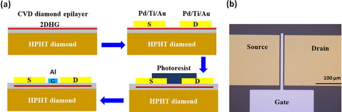
A laser lithographic technique was used for fabricating the SBDs and MESFETs. shows the devices fabrication process and the optical image of a typical diamond MESFET based on the H-terminated surface conductivity, respectively. Firstly, the source (S) and drain (D) electrodes patterns were defined by a photolithography process. The S-D electrodes were the multilayer Au/Ti/Pd (80/5/10 nm), which were deposited by using an electron-beam evaporator with a base pressure of ∼10−5 Pa. Pd was directly contacted to the H-terminated diamond surface. Secondly, an oxygen plasma was used to define the conductivity channel and isolate the devices by forming a mesa structure defined by the laser lithography process. Thirdly, an Al thin film (50 nm) was evaporated on the gate area as the Schottky contact patterned by the third laser lithography, which was deposited by using an electron-beam evaporator at the base pressure less than 10−7 Pa. After each step, the photoresists were removed by dipping the sample into a tetramethylammonium hydroxide (TMAH) solution and cleaned by deionized water. The gate length (Lg) was from 4–30 µm, the gate widths (Wg) were 50 µm and 100 µm. For the MESFETs, the spacing between the source or drain and gate electrodes (Lsg or Ldg) was from 4–30 µm. The source or drain electrodes and the gate electrode formed the Schottky diodes.
Figure 1. (a) Fabrication process of the diamond MESFETs based on the H-terminated diamond surface conductivity, including the growth of a CVD diamond epilayer, deposition of the Ohmic contacts, mesa formation for isolation, and gate deposition. (b) Optical image of a typical diamond MESFET.
Before and after the X-ray irradiation, both the SBDs and MESFETs were measured by using a probe station, which has an electrical current noise level less than 10−13 A. The current-voltage (I-V) characteristics of the SBDs and MESFETs were measured with different time durations spanned two weeks to examine the devices stability. The devices were irradiated by the X-ray in the air, which was generated by an X-ray generator (4037B; Rigaku Corp.) with a Cr target operated at 20 kV and 50 mA [Citation11]. The dose rate was 12 kGy/min and the total dose was 100 kGy, which was calibrated by using a cellulose triacetate film dosimeter (FTR-125; Fujifilm Corp.) before the irradiation on the diamond devices.
3. Results and discussion
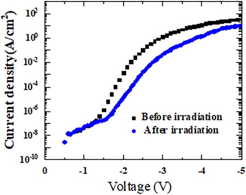
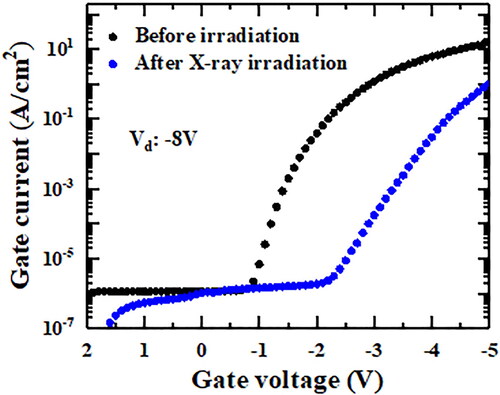
The forward I-V characteristics of the SBD before and after the X-ray irradiation in the MESFET structure is shown in . The leakage currents at reverses bias are extremely low and beyond the system detection limit of 10−13 A even after the X-ray irradiation. The rectifying ratio is as large as over 1010 before irradiation. Nevertheless, the forward current is reduced by over twice at the forward bias of −5 V after the irradiation. A fitting of the I-V curves shows that the ideality factor of the diode is much larger than unity. The large ideality factor is similar for the SBDs fabricated on the epilayers grown either on the type-IIa substrate or on the type-Ib substrate. Therefore, a tunneling process dominates the electrical transport and the present SBD actually behaves more like a metal-insulator tunneling diode. Note that the SBD with an ideality factor of near unity fabricated on a H-terminated diamond surface conductivity was reported with a much larger Al Schottky contact area [Citation12]. On the other hand, Kasu et al. found an interfacial layer between the metal and H-terminated diamond surface [Citation13]. This interfacial layer was observed to be amorphous-like, which might explain the nonideal I-V in the present SBDs. The natural oxidation of the Al metal edge and X-ray irradiation enhanced partial oxidation of the Al gate as well as the H-terminated diamond surface may also contribute to the reduction of the electrical current.
Figure 2. Current-voltage characteristic of the SBD on the type IIa diamond substrate before and after X-ray irradiation with a dose of 100 kGy.
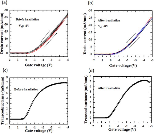
The electrical properties of the MESFET fabricated on the diamond epilayer grown on the type-IIa HPHT diamond substrate are shown in . The drain currents are normalized by the gate width Wg of 50 μm. The gate length of this device is Lg = 8 μm and the source-gate (Lsg) or gate-drain (Lgd) distance is 5 μm. The gate voltage (Vg) is varied from 0 to −5 V with a step of −0.5 V. The pinch-off characteristic is clearly observed. The drain current density is 27 mA/mm at the drain voltage of Vd = −10 V and gate voltage of Vg = −5 V before irradiation. The stability of the electrical properties of the MESFETs was investigated by two ways: repeated measurements and time dependent drain currents. Even after one week, the drain current changed little, as shown in . The drain current is highly reproducible and nearly the same after several times repeated measurements. After the irradiation by X-ray with a 100 kGy dose, the drain current is slightly reduced to 24 mA/mm at Vd = −10 V and Vg = −5 V. The on-resistance is increased from 167 Ωmm to 230 Ωmm at Vg = −5 V. The drain current as the gate voltage (Id-Vg) characteristics at Vd = −8 V before and after X-ray irradiation is illustrated in , respectively. A degradation in the drain current is clearly observed after irradiation, consistent with the data in . The gate voltage is repeatedly scanning from forward to reverse biases and then from reverse to forward biases. No hysteresis is observed and the curves are highly overlapped without dependence on the sweeping direction of the gate voltages for the MESETs before and after X-ray irradiation. The threshold voltage is about 0.4 V for the MESFET before irradiation, which changes little after X-ray irradiation. Therefore, the interface of the MESFET is nearly stable upon the X-ray irradiation, despite the existence of interface layer [Citation13]. The maximum transconductance of the MESFET is around 7 mS/mm, which experiences little degradation before and after the X-ray irradiation, as shown in . When the gate length was shrunk to 1 µm, the transconductance was increased to 110 mS/mm [Citation14]. Further reduction of the gate length to submicron greatly improved the transconductance over 200 mS/mm [Citation15,Citation16].
Figure 3. Current-voltage properties of the MESFET fabricated on the type-IIa diamond substrate. The device dimensions are Lg = 8 μm and Lsg = Ldg = 5 μm. (a) Electrical properties of the devices before the X-ray irradiation just after the device fabrication and after one week. (b) Electrical properties before and after the X-ray irradiation with a dose of 100 kGy.
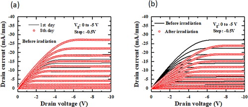
Figure 4. Drain current vs gate voltage of the MESFET fabricated on the type-Ib substrate with Lg = 4 μm and Lsg = Lgd = 6 μm before (a) and after (b) X-ray irradiation. Transconductance of the MESFET with before (c) and after (d) X-ray irradiation.
The gate leakage before and after X-ray irradiation is also investigated, as displayed in . The gate leakage is significantly reduced after the X-ray irradiation. The reduction of the leakage current by X-ray irradiation is reasonable considering the partial oxidation of the H-terminated surface and the oxidation of the edge of Al gate.
Figure 5. Gate-leakage at Vd = −8V of the MESFET fabricated on the type-IIa substrate before and after X-ray irradiation.
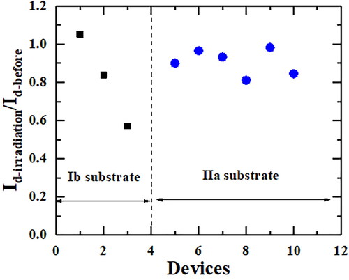
The effect of different types diamond substrates for the homoepitaxial diamond growth is also examined. Since the thickness of all the epilayers is less than 1 µm, the nitrogen effect in the substrate on the device properties are concerned here. Shown in is the electrical properties of the MESFET fabricated on the epilayer grown on the type-Ib diamond substrate. The dimensions of the MESFET are, Lg = 4 μm and Lsg = Ldg = 6 μm. The gate width is 100 μm. The reduction of the drain current and the increase in the on-resistance are also observed, similar to the devices fabricated on the epilayer grown on the type-IIa substrate, as shown in . The device shows a normally-off behavior with a threshold voltage around −0.78 V, which changes to −0.56 V after the X-ray irradiation, as shown in . Note a slight reduction of the drain current at the same Vd = −8 V and Vg = −5V occurs, which is due to the repeated measurements of the MESFET. However, it was confirmed that such kind of repeated measurement would not lead to a drastic reduction of the drain current like that of X-ray irradiation. At this moment, it is not clear on the factors determining the threshold voltages of the MESFETs fabricated on the type-Ib diamond substrate. The inhomogeneity in the crystal quality and nitrogen distribution across the epilayers are the possible mechanisms. Since the absolute drain currents of the devices varied from each by each, in , we plot the drain currents variation after the X-ray irradiation for different MESFETs fabricated on the epilayers grown on the type-IIa and type-Ib diamond substrates. The drain currents before irradiation are used as the references. It is revealed that the reduction of the drain currents of the MESFETs on the type-Ib diamond substrate is more scattered compared to those of the MESFETs on the type-IIa diamond substrate. Therefore, the nitrogen effect in the substate may also take an important role in the degradation of the device performance. The X-ray irradiation can ionize the nitrogen in the substrate and induce space charge or positive electrical field as a back gate for the MESFET, modifying the electrical field and thus reducing the drain currents. Suitable passivation of the H-terminated surface conductivity, improvement of the crystal quality, and investigation of nitrogen content in the diamond epilayer and substrate are necessary for further study. In the future, higher dose irradiation over 1 M Gy should also be investigated to see the reliability of the devices.
Figure 6. (a) Drain current vs gate voltage of the MESFET on the type-Ib substrate with Lg = 4 μm and Lsg = Lgd = 6 μm before and after X-ray irradiation. (b) Drain current vs gate voltage at Vd = −8V.
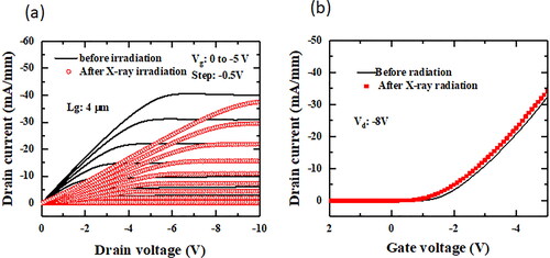
Figure 7. Variation of the drain current of the MESFETs as X-ray irradiation fabricated on the diamond epilayers grown on the type-IIa and type-Ib substrate. The drain currents before irradiation are used as reference. The gate voltage is Vg = −5V and the drain voltage is Vd = −8V.
4. Summary
The effect of X-ray irradiation on the SBD and MESFET fabricated on the diamond epilayers with hydrogen surface termination was investigated. A degradation in the drain current was observed for both of the epilayers grown on the type-IIa and type-Ib single-crystal diamond substrates. The threshold voltage experienced little change for the MESFET fabricated on the diamond epilayer grown on the type-IIa substrate. The reduction of the drain current was possibly attributed to the partial oxidation of the H-terminated surface and the edge of the Schottky gate. A passivation of the electrodes and the surface channel may enhance the radiation strength of diamond devices.
Disclosure statement
No potential conflict of interest was reported by the author(s).
Correction Statement
This article has been republished with minor changes. These changes do not impact the academic content of the article.
Additional information
Funding
Notes on contributors
Mingchao Yang
Dr. Mingchao Yang is now a lecturer in Hebei Normal University of Science and Technology, China. He received the doctor degree in physics science in Jilin University, China in 2019. His research includes diamond electronic devices and electrochemistry.
Takehiro Shimaoka
Dr. Takehiro Shimaoka is now a researcher in National Institute of Advanced Industrial Science and Technology (AIST), Japan. His research interest includes diamond growth and electronics.
Liwen Sang
Dr. Liwen Sang is an independent researcher in International Center for Materials Nanoarchitectonics (MANA), National Institute for Materials Science (NIMS), Japan. Her research interest includes the growth of wide-bandgap III-nitride semiconductors and semiconductor devices.
Junichi H. Kaneko
Dr. Junichi H. Kaneko is now an associate professor in Hokkaido University, Japan. His research interest includes diamond growth and nuclear physics.
Satoshi Koizumi
Dr. Satoshi Koizumi is now a group leader in National Institute for Materials Science (NIMS), Japan. His research interest includes diamond growth and n-type doping of diamond.
Meiyong Liao
Dr. Meiyong Liao is now a chief researcher in National Institute for Materials Science (NIMS), Japan. His research interest includes wide bandgap semiconductor materials (mainly diamond), photonic and electronic devices, MEMS/NEMS, and device physics.
References
- Liao M. Progress in semiconductor diamond photodetectors and MEMS sensors. Funct Diam. 2021;1(1):29–47.
- Sang L. Diamond as the heat spreader for the thermal dissipation of GaN-based electronic devices. Funct Diam. 2021;1(1):174–188.
- Umezawa H, Omagari S, Mokuro H, et al. Proceeding of the 29th International Symposium on power Semiconductor Devices and ICs; 2017. p. 379–382.
- Koike J, Parkin DM, Mitchell TE. Displacement threshold energy for type illa diamond. Appl Phys Lett. 1992;60(12):1450–1452.
- Liao M, Shen B, Wang Z. Ultra-wide bandgap semiconductor materials: semiconductor diamond. Oxford (UK): Elsevier; 2019.
- Seki Y, Hoshino Y, Nakata J. Remarkable p-type activation of heavily doped diamond accomplished by boron ion implantation at room temperature and subsequent annealing at relatively low temperatures of 1150 and 1300 °C. Appl Phys Lett. 2019;115(7):072103.
- Koizumi S. Growth and characterization of phosphorus doped n-type diamond thin films. Phys Stat Sol A. 1999;172(1):71–78.
- Kudara K, Imanishi S, Hiraiwa A, et al. High output power density of 2DHG diamond MOSFETs with thick ALD-Al2O3. IEEE Trans Electron Devices. 2021;68(8):3942–3949.
- Crawford KG, Maini I, Macdonald DA, et al. Surface transfer doping of diamond: a review. Progr Surf Sci. 2021;96(1):100613.
- Liao M, Sang L, Shimaoka T, et al. Energy-efficient metal–insulator–metal-semiconductor field-effect transistors based on 2D carrier gases. Adv Electron Mater. 2019;5(5):1800832.
- Yamaguchi T, Umezawa H, Ohmagari S, et al. Radiation hardened H-diamond MOSFET (RADDFET) operating after 1 MGy irradiation. Appl Phys Lett. 2021;118(16):162105.
- Tsugawa K, Noda H, Hirose K, et al. Schottky barrier heights, carrier density, and negative electron affinity of hydrogen-terminated diamond. Phys Rev B. 2010;81(4):045303.
- Kasu M, Ueda K, Kageshima H, et al. Gate interfacial layer in hydrogen-terminated diamond field-effect transistors. Diam Relat Mater. 2008;17(4-5):741–744.
- Umezawa H, Tsugawa K, Yamanaka S, et al. High-performance diamond metal-semiconductor field-effect transistor with 1 µm gate length. Jpn J Appl Phys. 1999;38(Part 2, No. 11A):L1222–1224.
- Ueda K, Kasu M, Yamauchi Y, et al. Using high-quality polycrystalline diamond with fT of 45 GHz and fmax of 120 GHz. IEEE Electron Device Lett. 2006;27(7):570–572.
- Yu C, He Z, Zhou C, et al. High frequency hydrogen-terminated diamond MESFET with an fmax of 103GHz. Mater Today Commun. 2021;28:102489.