
Abstract
Aiming at developing inch-sized processing of diamond, B-doped layer was grown on mosaic single-crystallin diamond wafers by using hot-filament chemical vapor deposition (CVD), which is expected to have an advantage in terms of the deposition area compared with microwave plasma (MWP) CVD. Uniformity in horizontal and vertical directions is studied. It is found that the junctions of the monocrystalline diamond domains in the mosaic wafer and the direction of the crystal off-angles against to these junctions are less effective to the uniformity of the impurity concentrations. On the other hand, it is suggested that excess incorporation of W from the filament suppresses the growth and incorporation of B. It is shown that millimeter scale or more precise control of the arrangement of the wafer and the filament enables to obtain more uniform and efficient doping.
Keywords:
1. Introduction
Several advantages in material constants of diamond are attractive for future applications such as power electronics and quantum technology [Citation1–4]. Realization of such applications by using this extreme material requires both of bulk wafers which have fine surface without critical crystal defects, and of high-quality epitaxial layers on them with controlled amounts of impurities. In addition, this requirement must be supported over inch-sized wafers for industrial use. Monocrystalline diamond with high quality could be produced by high-pressure-high-temperature method with a 12 mm diameter [Citation5], which is much smaller than those of other semiconductor materials, such as Si, SiC, and GaN [Citation2, Citation6]. In addition to such a mono-crystal diamond which are prepared on the single crystalline diamond seed, hetero-epitaxial diamond wafers [Citation7, Citation8], and mosaic diamond wafers [Citation9] with inch sized area have been reported and partially commercially available as well.
For processing especially of epitaxial growth and doping over such substrates/wafers of diamond, chemical vapor deposition (CVD) has been widely used [Citation1–4]. Especially, microwave plasma (MWP) CVD is a major technique especially for above mentioned applications, except for ion implantation technique with precise control of impurity [Citation10, Citation11]. On the other hand, hot-filament (HF) CVD is one of other options to prepare epitaxial layer owing to the advantage in the point of view of the growth-area which could by relatively easily extended and less soot formation even in the case of heavily doping [Citation12–14] unlike the case of MWPCVD [Citation15]. This method has been widely adopted for poly crystalline diamond coating aiming at various applications for example, mechanical tools, sealing, electrodes, MEMS/NEMS, and so on [Citation16, Citation17]. Recent reports show that this method could be applicable to the growth of homo-epitaxial layer on single crystal diamond substrates [Citation12–14]. Possibility to enhance device performance owing to the layer prepared by HFCVD is also shown [Citation12]. Furthermore, approaches to enhance the growth rate are also proposed [Citation18, Citation19].
There are some reports on uniformity of the growth and multi-dimensional distributions in the chamber [Citation16, Citation20–22], where most of them are focused on the poly crystalline diamond. Furthermore, report on B-doping for single crystalline diamond over large area is hardly found [Citation12], while this is indispensable processing for above mentioned future applications in electronics and quantum technology. In this work, B-doped layers are grown on the mosaic wafers by using HFCVD. Dependence of concentrations of impurity, B and W, on the distance from the filament and effect on the junctions of the monocrystalline diamond domain in the mosaic wafer are studied. Combined with the gas phase distributions of the temperature, which are calculated by computational fluid dynamic simulation under 3-dimensional model of the actual apparatus, importance how precise control of the location is discussed.
2. Experimental procedure
Boron doped diamond layers were grown on mosaic single-crystal diamond wafers, where the procedure to prepare them is described in our preceding works [Citation9, Citation23]. shows schematics of the arrangement of the filament and the wafers, which are placed in a commercial HFCVD reactor (sp3 Diamond Technologies, Inc., Santa Clara, CA). Extent of the filament was 400 mm square, which is much larger than the size of the mosaic wafers, ∼20 mm. As we will see from the result of the simulation, global distributions the gas temperature and the gas flow are sufficiently uniform and not expected to be a cause of the non-uniformity on the mosaic wafers. Distance between the filaments was kept 10 mm. In this study, three samples were prepared where the distances between the top surface of the substrates and the filaments were varied as 10, 7.5, and 5 mm by changing the thickness of the spacer as shown in . Filament temperature and gas pressure were kept 1950–2100 degrees in Celsius and 4 kPa, respectively, during the growth. Growth duration time was 20.5 h. Hydrogen, methane, and tri-methyl boron were introduced into the chamber during the growth as a source gas mixture, whose mass flow rates were 1000, 30, and 0.04 sccm, respectively. Growth rates of them were estimated from increment of the thicknesses which were measured by a micrometer. The concentrations of B and W in the grown layers were measured by the secondary ion mass spectroscopy (SIMS). These are summarized in . Concentrations of other major impurities such as hydrogen and nitrogen were not measured in this work. Katamune et al. [Citation24] showed very low amount of Nitrogen concentration close to the background level. Hydrogen concentration is also much lower than those of B in the present work. They used a (111) oriented substrate, which is known to incorporate relatively higher amounts of impurities than those of (100) oriented substrates as in the present work. Therefore, the amounts of those impurities in the present work are expected to be lower than those reported in this reference.
Figure 1. Schematic of the arrangement of the filament and the wafer. The thicknesses of the spacers with 0 (no spacer), 2.5, and 5 mm are tested in this work.
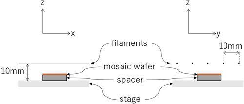
Table 1. Summary of the growth of the B-doped layers by using HFCVD in the present work.
3. Simulation procedure
ANSYS-Fluent was adopted to calculate the gas flow and temperature distributions in the HFCVD reactor as applied for MWPCVD [Citation25]. shows schematics of the 3-dimensional model structure, which corresponds to the actual structure for the growth experiments. The gas inlets and outlets are placed at the bottom and middle height of the chamber where the pure H2 with mass flow rate of 1slm is introduced. The diameter of the actual filament is submicron, which is too small to realize in the calculation domain. Therefore, horizontal voids with diameter of 2 mm are prepared 10 mm above the stage in the calculation domain. The inner walls of these voids correspond to the surfaces of the filaments. Because the Knudsen number is still large for the dimension of the distances between the filaments, this assumption is considered not to have serious effect on the present results. The boundary condition of 2000 or 3000 °C in Celsius is imposed on the walls to mimic the heated filament, as of the present work or the preceding work elsewhere [Citation18]. The temperatures of stage surface, the side and top walls are fixed to 600, 100, and 200 °C respectively. Just for simplicity, the source gas in the calculation is limited to pure hydrogen, which is treated compressible ideal gas.
4. Results and discussion
As shown in , the growth rates are higher for the shorter distance between the top surface of the substrate and filament. Likewise, B-concentrations are also higher for higher growth rate. One may notice that the growth rate on the junctions among the mono-crystals is slightly higher than that in the location off the junction. This correspondence between the growth rate and the B concentration is consistent with those reported in the preceding work [Citation13].
shows the pictures of the samples after the growth, which were transparent before the growth as shown in our preceding work [Citation23]. The maximum dimensions of these samples are about 20 mm. Black and red arrows represent location of the filament during the growth and the junction of the mono-crystals, which are constituents of those mosaic substrates. It is clear that the sample is darker for higher B concentration.
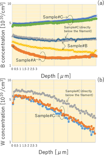
Shows depth profiles of the (a) B and (b) W concentrations of the three samples, which was measured by SIMS. B concentration increases with by shortening the distance between the top surface of the substrate and filament. All the samples have the same order of the magnitudes. Though, its variation is from 1 to 6 × 10²⁰/cm3, which corresponds to several 100/Ωcm [Citation26]. The junctions of the monocrystalline diamond in the mosaic wafer are less effective to the concentration than the distance between the top surface of the substrate and filament, which were tested here. In the case of the crystal quality grown by MWPCVD, which were evaluated by using Raman spectroscopy for example, is known to be affected by the relationship of directions of the junctions of the monocrystalline diamond in the mosaic wafer to the off-directions [Citation23]. As listed in , the relationship of these directions is also varied and not so effective to the concentration. The area directly below the filament (Sample#C, crosses colored in turquoise blue), B concentration is lower than those on the area which are in the distance 5–10 mm from there (Sample#C, ×symbols and dots colored in light blue and green, respectively). While the temperature in the gas phase and substrate are expected to be higher in the region directly below the filament than those of other area, we will see that this might not be the most important cause to explain this non-uniformity. Therefore, it is expected that there are some other obstructive factors to suppress the B incorporation.
In addition to the absolute values of the concentrations, depth profile itself is also affected by the distance. In the case of the farthest case (Sample#A), the B concentration decreases with the depth, but in the case of the closest case (Sample#C), the concentration gently increases with the depth. This suggests importance of the moderate distance to obtain uniform concentration in the direction to the growth.
W concentration is expected to be highest as well for the closest case, ie, Sample#C. shows W concentrations of this case. First, this result suggests that W concentration is not so affected by the junctions of the monocrystalline diamond in the mosaic wafer as well. Second, the location against to the filament has more remarkable effect. Opposite to the case of B, W concentration directly below the filament is slightly higher than those of other area. W decreases with depth at the all locations (, which is also opposite trend of B concentrations (. The concentration has steeper profile in the direction to the growth.
shows the Raman spectra of the (a) samples #A and #B, and (c) sample#C after the growth, where the wavelength for the excitation was 457 nm (Hriba, JOBIN YVON T64000). While these signals include those from the substrates, the slight increase in the lower side of the wave number corresponds to the increment of the B concentration [Citation27]. As B concentrations increases, the symmetricity of the spectra degraded [Blue and orange lines in for Sample#B, and grey line of for Sample#C] and eventually highly asymmetric profile is obtained (blue and orange lines in for Sample#C).
We found that there are line structures along with the filament was formed on the top surface at the region directly blow the filament after the growth in the case of Sample#C. shows the line profile in the direction perpendicular to the line structure, where an interference microscope (R3300HL-Lite, Ryoka Systems Inc., Tokyo, Japan) was utilized for the measurement. As shown in , the growth was suppressed directly below the filament in the case that the substrate is very close to the filament (Sample#C). Such structure was not found in the cases of the Samples#A and B.
To consider the effect of the gas phase, we shall look at the distributions of the gas temperature and flow. shows global distributions of them. Except for the region near the edges of the outer most filament in y-direction, temperature, and gas flow seem to be uniform. This is similar to the results reported elsewhere [Citation21] and seems to have improved uniformity than that in some report [Citation20]. Except for the local variation around the filament, millimeter-scale non-uniformity is not observed in horizontal direction around the stage. Vertical component of the gas flow is dominant in inner region. In the edge region, where is close to the outer most filament, horizontal component of the gas flow is enhanced. Though, scale of these non-uniformity is larger than the distance between the filaments and comparable to the stage and extent of whole the filaments.
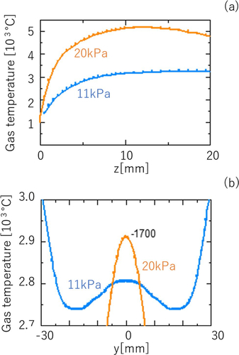
shows (a) vertical and (b) horizontal distributions of the gas temperature for the HFCVD chamber of this study, where vertical profiles are at the plane along with the filament, and the horizontal profiles are at the height 5 mm above the stage/below the filament. For comparison, the distributions of the gas temperature in the case of the MWP are also shown in , where the gas pressure, 11 and 20 kPa, are relatively higher, than that of the study here for the HFCVD, 4 kPa. As one possibility, the temperature non-uniformity is attributed to one of the possible causes of the suppression of the growth which were observed for Sample#C. Temperature gradient is steeper in the direction of the growth ( than the horizontal direction (. However, compared with the case of MWP (, temperature gradient is rather gentle. The non-uniformity in the horizontal direction in the case of HF is limited to several 10 degrees (, which is smaller variation than that of the MWP ( as well. Especially in the case of the MWP with elevated gas pressure, even in the 1 inch diameter, there exist several 100 degrees of temperature variation. This is the biggest reason to make difficult to obtain uniform growth for the case of MWP [Citation9, Citation28].
Temperature is higher in region closer to the filament. Higher gas temperature may promote enhancement of production of the radical and therefore growth rate. Therefore, as we saw in concentration increases with shortening the distance between the filament and top surface of the substrate. In the case of the MWP, this causes non-uniformity of the growth rate in the horizontal direction [Citation28, Citation29]. On the other hand, in the case of HFCVD, as we saw in , the growth directly below the filament was suppressed in the case with closest distance between the filament and the top surface of the wafer (Sample#C). Therefore, non-uniformity in gas-phase temperature distribution is unlikely to be a main cause of non-uniformity of the impurities directly below the filament in the case with smaller distance between the substrate and the filament.
Figure 2. (a), (b)Schematics of the is the 3-dimensional model structure, which corresponds to the actual structure for the growth experiments, and (c) mesh arrangements near the region of the voids. The voids in the calculation domain correspond to the filament. Temperature of these inner walls of these voids is set to be 2300 or 3100 °C.
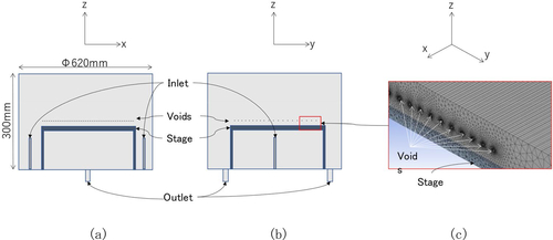
Figure 3. Pictures of the samples after the growth, which were transparent as shown in our preceding works [Citation24]. Black and red arrows represent location of the filament during the growth and the junction of the mono-crystals, which are constituents of those mosaic substrates.
![Figure 3. Pictures of the samples after the growth, which were transparent as shown in our preceding works [Citation24]. Black and red arrows represent location of the filament during the growth and the junction of the mono-crystals, which are constituents of those mosaic substrates.](/cms/asset/3bbebf77-defc-4b98-a322-52692f6d5030/tfdi_a_2068972_f0003_c.jpg)
Figure 4. Depth profiles of (a) B and (b) W measured by SIMS.
Combined with the growth experiments and the results of the calculation, above results suggest that the excess incorporation of W suppress the B concentration. This is consistent with the inverse correlation between the depth profiles of B and W in the case of the closest case (Sample#C). A preceding work gives correlation between the growth rate and the B concentration in the gas phase, which also has correlation with the concentration in the CVD layer [Citation14, Citation15]. The temperature directly below the filament is also relatively higher than that of the other regions, even several 10 degrees, the concentrations of B-related precursors directly below the filament are expected to be higher than those in the other regions. On the other hand, if the sample is too close to the filament, effect of W to hinder the growth and B incorporation becomes remarkable. This might be more effective than that of the enhancement of the production of precursors. The locations of the SIMS measurements of Sample#C which is not directly below the filament are in 5 mm distance or more from that region. This implies that the lifetimes of the W-related precursors are not so long, and its amount converges into a certain level within a short distance.
From above result, the distance between the substrate top surface and the filament larger than 5 mm is considered to give uniform distribution of the impurity concentration. This distance may be increased with increase of the filament temperature (. On the other hand, depending on the fluctuation of the filament temperature, such as 100 °C may cause the non-uniformity in direction to the growth. This might be also controlled by the distance between the filament and the top surface of the substrate. In some cases, shortening of this distance promotes uniform concentration in the direction of the growth.
Figure 5. Raman spectra of the (a) samples #A and #B, and (c) sample#C after the growth.
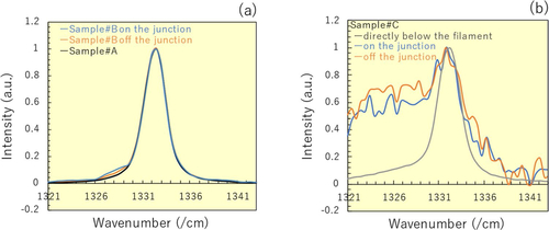
Figure 6. Profile in direction perpendicular to the line-structure of Sample#C, which was formed after the growth along with the filament.
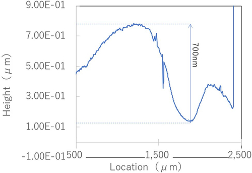
Figure 7. Global distributions of (a) gas temperature and (b) flow.
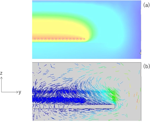
Figure 8. Profiles of the gas temperature in the (a) vertical on the axis perpendicular to the filament and (b) horizontal direction at the height 5 mm below the filament, which were calculated for the HFCVD apparatus.
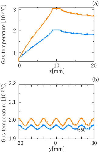
Figure 9. Profiles of the gas temperature in the (a) vertical on the central symmetric axis perpendicular to the substrate and (b) horizontal direction at the height 5 mm above the substrate top surface for the case of MWPCVD.
5. Summary
Horizontal and vertical uniformity of impurity concentrations in HFCVD layers were studied by using mosaic single-crystalline diamond wafers. The junctions of the monocrystalline diamond in the mosaic wafer and its direction to the crystal off-angles were found to be less effective to the uniformity of the concentration. Concentrations of B for the case closer to the filament are higher, but the region directly below the filament has relatively suppressed concentration. Numerical simulation shows that temperature distribution near the filament has some non-uniformity, which is smaller than that of MWP. From the inverse relationship with the corresponding B concentration and gas-phase temperature distributions, this result implies that excess incorporation of W suppresses the growth and the incorporation of B. Millimeter scale or more precise control of the wafer and filament arrangement enables to achieve more efficient growth of the uniform B doped layer by using HFCVD.
Disclosure statement
No potential conflict of interest was reported by the authors.
Additional information
Funding
References
- Doping and semiconductor characterizations. In: Koizumi S, Pernot J, Umezawa H, Suzuki M, editors. Power electronics device applications of diamond semiconductors. Sawston: Woodhead Publishing; 2018. pp. 99–189.
- Donato N, Rouger N, Pernot J, et al. Diamond power devices: state of the art, modelling, figures of merit and future perspective. J Phys D Appl Phys. 2020;53(9):093001.
- Achard J, Jacques V, Tallaire A. Chemical vapour deposition diamond single crystals with nitrogen-vacancy centres: a review of material synthesis and technology for quantum sensing applications. J Phys D Appl Phys. 2020;53(31):313001.
- Zheng Y, Li C, Liu J, et al. Chemical vapor deposited diamond with versatile grades: from gemstone to quantum electronics. Front Mater Sci. 2022;16(1):220590.
- Sumiya H, Tamasaku K. Large defect-free synthetic type IIa diamond crystals synthesized via high pressure and high temperature. Jpn J Appl Phys. 2012;51:090102.
- Tsao JY, Chowdhury S, Hollis MA, et al. Ultrawide‐bandgap semiconductors: research opportunities and challenges. Adv Electron Mater. 2018;4(1):1600501.
- Schreck M, Gsell S, Brescia R, et al. Ion bombardment induced buried lateral growth: the key mechanism for the synthesis of single crystal diamond wafers. Sci Rep. 2017;7:44462.
- Kim SW, Takaya R, Hirano S, et al. Two-inch high-quality (001) diamond heteroepitaxial growth on sapphire (1120) misoriented substrate by step-flow mode. Appl Phys Express. 2021;14(11):115501.
- Yamada H, Chayahara A, Mokuno Y, et al. A 2-in. mosaic wafer made of a single-crystal diamond. Appl Phys Lett. 2014;104(10):102110.
- Seki Y, Hoshino Y, Nakata J. Extremely high-efficient activation of acceptor boron introduced by ion implantation at room temperature with various doping concentrations in epitaxially synthesized diamond films by chemical vapor deposition. J Appl Phys. 2021;129(19):195702.
- Haruyama M, Onoda S, Higuchi T, et al. Triple nitrogen-vacancy Centre fabrication by C5N4Hn ion implantation. Nat Commun. 2019;10(1):2664.
- Ohmagari S, Yamada H, Tsubouchi N, et al. Schottky barrier diodes fabricated on diamond mosaic wafers: dislocation reduction to mitigate the effect of coalescence boundaries. Appl Phys Lett. 2019;114(8):082104.
- Ohmagari S, Ogura M, Umezawa H, et al. Lifetime and migration length of B-related admolecules on diamond {1 0 0}-surface: comparative study of hot-filament and microwave plasma-enhanced chemical vapor deposition. J Crystal Growth. 2017;479:52–58.
- Ohmagari S, Srimongkon K, Yamada H, et al. Low resistivity p + diamond (100) films fabricated by hot-filament chemical vapor deposition. Diamond Relat Mater. 2015;58:110–114.
- Tokuda N, Umezawa H, Saito T, et al. Surface roughening of diamond (001) films during homoepitaxial growth in heavy boron doping. Diamond Relat Mater. 2007;16(4–7):767–770.
- Schäfer L, Höfer M, Kröger R. The versatility of hot-filament activated chemical vapor deposition. Thin Solid Films. 2006;515(3):1017–1024.
- Auciello O. Science and technology of a transformational multifunctional ultrananocrystalline diamond (UNCDTM) coating. Funct Diamond. 2022;2(1):1–24.
- Takamori Y, Nagai M, Tabakoya T, et al. Insight into temperature impact of ta filaments on high-growth-rate diamond (100) films by hot-filament chemical vapor deposition. Diamond Relat Mater. 2021;118:108515.
- Tabakoya T, Kanada S, Wakui Y, et al. High‐rate growth of single‐crystalline diamond (100) films by hot‐filament chemical vapor deposition with tantalum filaments at 3000 °C. Phys Status Solidi A. 2019;216(21):1900244.
- Wu Y, Zhang H, Yan G, et al. Hot filament chemical vapor deposition temperature field optimization for diamond films deposited on silicon nitride substrates. Mater Res Express. 2021;8(11):116403.
- Alcantar-Peña JJ, Montes J, Arellano-Jimenez MJ, et al. Low temperature hot filament chemical vapor deposition of ultrananocrystalline diamond films with tunable sheet resistance for electronic power devices. Diamond Relat Mater. 2016;69:207–213.
- Zhang T, Qian Y, Wang S, et al. Influence of the heat dissipation mode of long-flute cutting tools on temperature distribution during HFCVD diamond films. Crystals. 2019;9:394.
- Yamada H, Chayahara A, Umezawa H, et al. Fabrication and fundamental characterizations of tiled clones of single-crystal diamond with 1-inch size. Diamond Relat Mater. 2012;24:29–33.
- Katamune Y, Mori D, Arikawa D, et al. n-Type doping of diamond by hot-filament chemical vapor deposition growth with phosphorus incorporation. Appl Phys A. 2020;126(11):879.
- Yamada H. Numerical simulations to study growth of Single-Crystal diamond by using microwave plasma chemical vapor deposition with reactive (H, C, N) species. Jpn J Appl Phys. 2012;51:090105.
- Bustarret E, Gheeraert E, Watanabe K. Optical and electronic properties of heavily boron-doped homo-epitaxial diamond. Phys Stat Sol (a). 2003;199(1):9–18.
- Issaoui R, Tallaire A, Mrad A, et al. Defect and threading dislocations in single crystal diamond: a focus on boron and nitrogen codoping. Phys Status Solidi A. 2019;216(21):1900581.
- Yamada H, Chayahara A, Ohmagari S, et al. Factors to control uniformity of single crystal diamond growth by using microwave plasma CVD. Diamond Relat Mater. 2016;63:17–20.
- Yamada H, Chayahara A, Ohmagari S, et al. Effect of Ar addition on uniformity of diamond growth by using microwave plasma chemical vapor deposition. Diamond Relat Mater. 2018;87:143–148.