
Abstract
Diamond is an ultrawide bandgap semiconductor with excellent electronic and photonic properties, which has great potential applications in microelectronic and optoelectronic devices. As an allotrope of diamond, graphene also has many fantastic properties like diamond, which caught much attention in combing them together. In this work, a direct sp3-to-sp2 conversion method was proposed to fabricate graphene layers on single crystal diamond by thermal treatment with Ni film catalyst. By optimizing the conversing conditions, a thin graphene layer with low sheet resistance was obtained on diamond. Based on this, an all-carbon sandwich structural graphene-diamond-graphene (GDG) detector was fabricated, which shows low dark current of 0.45 nA at 0.5 V μm−1 applied electric field. The maximum sensitivity of this detector is obtained when the incident X-ray is 12 keV, with the value of 2.88 × 10⁻⁸ C Gy−1. Moreover, the rise time and delay time of the GDG detector is about 1.2 and 22.8 ns, respectively, which are very close to that of diamond detector with Ti/Au electrode. The realization of the direct in-situ sp3-to-sp2 conversion on diamond shows a promising approach for fabricating diamond-based all-carbon electronic devices.
1. Introduction
Diamond is an ultrawide bandgap semiconductor showing great potential applications in radiation detectors and particle physical applications, due to its fantastic properties, such as ultrawide bandgap (5.47 eV) [Citation1,Citation2], high carrier mobility (4,500 and 3,800 cm2 V−1 s−1 for electrons and holes, respectively) [Citation3], high breakdown field (≈107 V cm−1) [Citation4,Citation5] and high radiation hardness [Citation6,Citation7]. Compared to other semiconductors, like Si, Ge and GaAs, diamond devices can operate under a temperature and radiation hardness high up to 500 °C and 1015 ions cm−2, respectively, where devices made of traditional semiconductors do not have a long-term durability [Citation8,Citation9]. In the early 1950s, natural diamond was selected to fabricate X-ray, electron, proton, and neutron detectors [Citation10,Citation11]. However, the non-producibility, uncontrollable defects and impurity concentrations of natural diamond restrict its further applications in electronic devices [Citation12,Citation13]. In recent years, with the mature of synthesis technology of artificial diamond through chemical vapor deposition (CVD) and high-pressure high-temperature (HPHT) method, single crystalline diamond with large size and low impurities can be synthesized both in laboratory and industry [Citation14]. Especially, diamond synthesized by microwave plasma chemical vapor deposition (MPCVD) method can have an ultrahigh purity with impurity concentration <5 ppb, which further pushes the investigation of diamond semiconductors in electronic and optoelectronic devices.
High purity CVD diamond is regarded as the ideal material for fabricating highly energetic radiation detectors owing to the wide band gap and high radiation hardness. For the demand of sensitivity and time responsivity, diamond radiation detectors are usually fabricated in sandwich structure with metals as electrodes, such as Ti/Au, and Cr/Au [Citation15,Citation16]. Graphene, as an allotrope of diamond, has many fantastic properties like diamond, such as high thermal conductivity (≈5,300 W m−1 K−1) [Citation17], high carrier mobility (≈20,000 cm2 V−1 s−1) [Citation18] and high radiation hardness [Citation19]. Recently, it has caught wide attention to be used as the electrode materials in electronic devices [Citation20–22]. Compared to conventional metal electrode, graphene has low atomic number and resulting low absorption and beam scattering of UV and X-ray radiations, which make it an excellent choice of electrode materials for a transmissive UV and X-ray detectors. For example, Wei et al. [Citation23] fabricated a diamond UV detector with graphene as front electrode, the introduction of the graphene electrode achieved high responsivity and gain factor in solar-blind sensing. Besides, both graphene and diamond have high thermal conductivity and high radiation harness, which promise great potential of their applications working in high temperature and harsh environment with high radiation dose. Due to the above excellent properties, the combination of graphene and diamond would promote the synergy of them in graphene-diamond heterostructure devices.
Usually, for most graphene electronic and optoelectronic devices, graphene films were grown on metal substrate via CVD method and then transferred to the target substrate with the assistance of PMMA [Citation24]. However, impurities and damages cannot be avoided during the transfer process, leading to the degradation of graphene properties [Citation25]. In order to overcome this, carbon-containing substrate SiC is annealed under high temperature (>1300 °C) to induce the formation of graphene on SiC surface [Citation26]. Inspired by this, Tokuda et al. achieved graphene layers on diamond surface through direct vacuum annealing at a temperature over 1100 °C [Citation27]. However, the obtained graphene layers on diamond are uncontrollable during this graphitization process. To obtain controllable graphene layers on diamond, transition metal catalysis, like Cu and Ni, are employed to induce the formation of graphene layers on the diamond surface. For the diamond samples coated a thin Cu [Citation28] or Ni film [Citation29–31], the carbon atoms on diamond surface transform from sp3-hybridization to sp2-hybridization, leading to the formation of graphene on diamond surface under a treatment temperature among 800–1000 °C. The direct conversion of graphene on diamond promises the fabrication of diamond devices with graphene as the electrodes.
In this work, a sandwich structural diamond X-ray detector was fabricated with direct sp3-to-sp2 conversed graphene layers as electrodes. The graphene layers were fabricated by thermal treatment of Ni coated diamond, in which the carbon atoms on diamond surface transferred from sp3-hybridization to sp2-hybridization. The fabricated graphene-diamond-graphene (GDG) all-carbon detector shows a low dark current of 0.45 nA at 0.5 V μm−1 applied electric field, and good response to 3–20 keV incident X-ray photons. Moreover, the maximum sensitivity of the diamond detector was obtained at 12 keV incident photons, with a responsivity of 2.88 × 10⁻⁸ C Gy−1 at 0.5 V μm−1. Moreover, the rise and delay time of the GDG detector is about 1.2 and 22.8 ns, respectively, which are very close to that of diamond detector with Ti/Au electrode. The successful fabrication of direct sp3-to-sp2 conversion of graphene on diamond surface provide a possible method for the development of diamond based all-carbon radiation detectors.
2. Methods
2.1. Materials
High-quality single-crystal CVD diamond (B and N impurities: < 1 and 5 ppb, respectively) with the size of 4.5 × 4.5 mm2 and thickness of 300 μm was obtained from Element Six Ltd., UK. The high purity (99.995%) Ni for electron beam deposition was purchased from Zhongnuo Advanced Material Co. Ltd., China. The chemical reagents, such as hydrogen peroxide (30%), sulfuric acid (98%), hydrochloric acid (36–38%), ethanol, and CuSO4·5H2O were all analytical grade and purchased from Sinopharm Chemical Reagent Co. Ltd., China.
2.2. The graphene growth
Before thermal treatment, diamond substrate was immersed in the mixture of H2SO4 and H2O2 solution (2: 1 in volume) at 80 °C for 4 h to remove the surface impurities. A 15-nm-thick Ni film was then deposited on the both sides of the diamond at a deposition rate of 0.5 Å s−1 in an e-beam deposition system (MUE-ECO, Japan), at a background pressure of 2.0 × 10⁻³ Pa. To covert sp3-boned carbon on the diamond surface into sp2-hybridized atoms, the Ni-coated diamonds were then treated at 950–1050 °C for a certain time in a tube furnace system (BTF-1200C-II-SL, Anhui BEQ Tech., China) with an 8 sccm H2 flow and 100 sccm Ar flow. After thermal treatment, the Ni residual on the diamond surface was removed by an etching solution (CuSO4: HCl = 10 g: 50 mL in 50 mL deionized water). At last, another thermal treatment can be performed under 600 °C in air for only 10 min to remove the unexpected graphite formed on the side edge of the above diamond sample, if necessary.
2.3. Characterizations
The quality of diamond and graphene was characterized by Raman spectrometer (Renishaw plc, Wotton-under-Edge, UK) with 532 nm excitation wavelength of He–Ne laser. The ultraviolet visible (UV-Vis) transmittance of the diamond sample was characterized by a UV-Vis spectroscopy (Lambda 950, Perkin-Elmer, USA). Field emission scanning electron microscopy (SEM, QUANTA 250 FEG, FEI, USA) and transmission electron microscopy (TEM, JEOL JEM-2100, Japan) were used to investigate the surface morphology and microstructure of the diamond-graphene interface. 60 kV X-ray source (MAGPRO, Moxtek, USA) with an output power of 12 Watts was employed to study the performance of diamond-graphene heterostructure detector, and the electrical response under X-ray irradiation was measured by a precision source/measure unit (B2902A, Agilent Technologies, USA). During time response test, the X-ray source used here is Golden XRS-3 (Golden Engineering Inc, USA) portable X-ray source, and the signal was captured by an oscilloscope (4456E, Ceyear Technologies Co., Ltd, China).
3. Results and discussions
3.1. Sp3-to-sp2 conversion and characterization
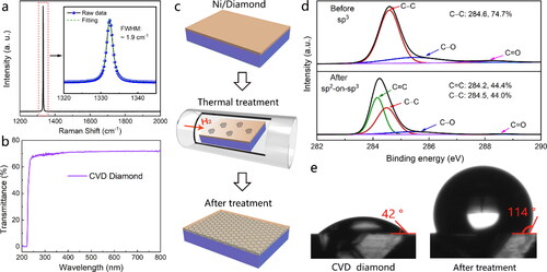
The properties of the CVD diamond before catalytically thermal treatment were characterized in . On the Raman spectra in , only the intrinsic peak of diamond at 1332.4 cm−1 can be observed, with the full width at half maximum (FWHM) of about 1.9 cm−1. Moreover, the transmittance of the CVD diamond is about 71.8% in the visible region and 68% at 238 nm as shown in , corresponding to the theoretical values of the pure diamond. The above Raman spectra and the UV-Vis transmittance indicate the good crystallinity and high purity of CVD diamond. The carbon sp3-to sp2-conversion process using a thin Ni layer as catalyst was schematically illustrated in . After thermal treatment, the carbon atoms on the diamond surface transform from sp3 to sp2 hybridization with the assistance of Ni catalyst. The specie and content of the carbon bonds on diamond surface before and after thermal treatment were characterized by XPS analysis, as shown in . According to the specific C 1 s spectra, it can be clearly observed that there are three carbon peaks (C–C, C–O and C = O) on the diamond surface. The high C–C content (74.4%) indicates that besides the oxygen containing groups, pristine diamond surface is composed of all sp3 bond. After thermal treatment, the content of C–C bond nearly halved, while the proportion of C = C bond increased to 44.4%, indicating the carbon sp3-to-sp2 conversion occurred on diamond surface [Citation32]. Meanwhile, as the content of oxygen containing groups nearly halved from 20.9% to 11.6% after thermal treatment, the water contact angle on diamond surface increased from only 42° to about 114° after sp3-to-sp2 conversion process, as shown in , which was caused by the hydrophobicity of the diamond-graphene surface.
Figure 1. (a) Raman and (b) UV-Vis transmittance characterization of CVD diamond, (c) experimental scheme of carbon sp3-to-sp2 conversion on diamond surface, (d) C 1 s spectra and (e) water contact angle of diamond surface before and after thermal treatment.
3.2. Characterizations of graphene formed on diamond
In order to invstigate the influence of conversion parameters on the quality and layer numbers of graphene formed on diamond substrate, the thickness of Ni films (10, 15, 25, 50 and 100 nm), treatment temperature (950, 1000, and 1050 °C) and treatment time (10, 15, and 20 min) are systematically investigated. As shown in and Figure S1, the typical peaks of graphene can be found at 1585 (G-band) and 2712 cm−1 (2 D-band), respectively. The appearance of G-band originates from the sp2-hexagonal hybridization of carbon atoms, and the 2 D-band is caused by second-order two phonon scattering and sensitive to the layer number of graphene stacking [Citation33]. According to , , when the thickness of Ni films is smaller than 15 nm, a sharp peak can also be founded at ≈1332 cm−1, which is the typical peak of single crystalline diamond [Citation34]. Similarly, the peak of diamond can be also found when the treatment temperature is lower than 1000 °C () and the treatment time is smaller than 15 min (Figure S1a, b). The observation of the strong diamond peak indicates the formed graphene on diamond surface is thin enough that the laser can transmit the graphene layers to the diamond substrate. With the increase of Ni film thickness, treatment temperature and treatment time, the peak of diamond gradually weakened and finally disappeared, while the D-band (at ≈1350 cm−1) of graphene became obvious, as shown in . The absence of the diamond peak and appearance of D-band can be attribute to that with the increase of the thickness of Ni film, the graphene layers formed on the diamond became from incomplete to full coverage, even with some defects [Citation29].
Figure 2. Raman spectra of graphene formed on the diamond surface after different treatment temperature at (a) 950 °C, (b) 1000 °C, (c) 1050 °C; (d) I2D/IG ratio and (e) FWHM of 2 D-band of the graphene under different conversing conditions; (f) TEM image of obtained graphene through the optimal condition.
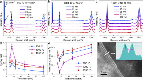
The relation of the I2D/IG ratio and the full width at half maximum (FWHM) of 2 D-band of the graphene on diamond surface as a function of the conversion parameters were represented in . At each temperature, the I2D/IG ratio (FWHM of 2 D-band) firstly increases (decreases) with an increase of Ni thickness and reached the maximum (minimum) value when Ni thickness is 15 nm, then it decreases (increases) with a further increase of Ni thickness. The change tendency of the curves of I2D/IG ratios and FWHM of 2 D-band can be explained that the coverage of graphene on diamond become from incomplete (Ni: 10 nm) to complete (Ni: 15 nm), and further, to thicker with the increase of Ni film thickness. Typically, for each thickness (, ), the I2D/IG ratios and FWHM of 2 D-band always have the maximum and the minimum value when the temperature is 1000 °C, respectively. As a result, the optimized sp3-to-sp2 conversion condition was finally obtained with 15 nm-thick Ni film, 1000 °C treatment temperature and 15 min treatment time (in , and Figure S2). Under this optimized condition, the I2D/IG ratios and 2 D-band FWHM reach the values of ≈1.3 and ≈43 cm−1, respectively, corresponding to 2–3 layers of graphene [Citation35]. The layers of the graphene formed on diamond surface at optimized condition was also characterized by TEM images, in which the few-layer graphene can be clearly observed, as shown in .
3.3. Comparison and simulation of different graphene-diamond interface
The interface properties of direct graphene on diamond and on hydrogen-terminated diamond (H-diamond) structure were computed based on density-functional theory (DFT). When a CVD grown graphene layer is transferred onto the diamond surface, a hydrogen termination layer may exist at the graphene-diamond interface, leading to the formation of graphene-H-diamond heterostructure [Citation36]. However, in this work, the graphene-diamond heterostructure was fabricated by direct sp3-to-sp2 conversion, and the graphene is in direct contact with the diamond substrate, without a hydrogen layer inserted between them. To compare them, the DFT is applied in this work to calculate the interface properties of graphene on diamond and graphene on H-diamond structures, with the calculation models shown in , , respectively. In each model, there are three graphene layers on the diamond (100) and H-diamond (100) surface, and the bulk diamond is composed of 12 atomic layers of carbon atom. After the optimization of graphene/diamond structure, the corresponding lattice constant mismatch is 1.29%, and vacuum buffer layer is greater than 15 Å in each supercell. The nearest neighboring graphene carbon layer shows a lattice deformation, no longer maintaining a 2 D structure on the diamond surface, as shown in , such surface reconstruction initiates a step-by-step conversion of the topmost diamond layer to graphene due to the structural and bonding changes under high vacuum conditions at high temperature [Citation37].
Figure 3. Simulation model of (a) diamond graphene structure and (b) H-diamond graphene structure; the corresponding total electron density distributions of (c) diamond graphene structure and (d) H-diamond graphene structure; and the Flat band structure of graphene supported on the (e) diamond surface and (f) H-diamond. The blue and red colors stand for the contribution from graphene, and diamond, respectively.
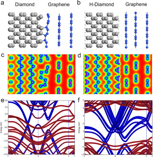
The calculation results reveal that the interlayer distance is 1.64 Å between the neighboring diamond and graphene layers in , which is much smaller than that between the individual graphene layers (3.38 Å). However, when a hydrogen termination layer exists on the diamond surface, the H-diamond exhibits weak Van der Waals interactions with the graphene layers, resulting in an equilibrium spacing of 2.34 Å for the graphene/H-diamond interface, as shown in . Meanwhile, the graphene layer on the H-diamond surface can still maintain the 2 D structure due to the weaker van der Waals force. However, when graphene and diamond contact directly, a reconstitution of the nearest graphene layer on diamond occurred. The total electron density distributions of the graphene on diamond and H-diamond heterostructure are plotted in , . The electrons, accumulated at the graphene on diamond interface as shown in , suggests the formation of covalent bonds between the interface based on large orbital overlapping, thus leading to a strong interfacial interaction. This is contrary to the lack of an electron accumulation at the graphene/H-diamond interface, as shown in , which contacts by van der Waals interactions. As a result, direct graphene on diamond contact can be expected to have a much higher electron injection efficiency than the case of the graphene on H-diamond contact. Besides, according to the flat band structure shown in , , the Dirac point and band structure of graphene (blue lines) have few changes in both structures due to the slight orbital hybridization between both graphene and diamond/H-diamond surface. Strong band hybridization is found in clean diamond in , which induces to the band of diamond crossing the Fermi level. However, when hydrogen exists on diamond surface in , there is still a large band gap of over 3.0 eV for diamond.
3.4. Fabrication of GDG devices and its response to X-ray irradiations
A graphene-diamond-graphene (GDG) sandwich structural device was obtained by forming graphene layers on the double sides of diamond through the above direct sp3-to-sp2 conversion process. A GDG X-ray detector was then fabricated using the sp3-to-sp2 conversed graphene layers (area: ≈20 mm2) as the front and back electrodes, as schematically illustrated in . The dark current of the devices was about 0.45 nA at a forward bias of 150 V (at 0.5 V μm−1), corresponding to a current density of 2.22 nA cm−2 at the bias of 0.5 V μm−1, as shown in . Due to the high resistance of intrinsic diamond, a space-charge effect occur on diamond surface, leading to the nonlinearity on the IV curve in the -10 − 10 V region, which could be avoid by forming a thin diamond like layer (DLC) on the diamond and graphene interface [Citation38]. According to the theory calculation, the direct conversed graphene has strong interface interaction with diamond. However, the calculated barrier height through thermionic emission equation is about 0.953 eV (Figure S3), which is close to the literature reports [Citation23]. Besides interfacial defects that leading to a strong space-charge effect, the high barrier height was also caused by the surface state of the diamond [Citation39], which can be also demonstrated by the specific contact resistance measurement of different electrode on diamond substrate (as shown in Figure S4).
Figure 4. (a) Structure of the proposed diamond-graphene X-ray detector, (b) dark current of the proposed diamond detector, the sensitivity of the diamond detector (a) as a function of applied voltage under different X-ray energy (3–20 keV), and (d) as a function of incident X-rays with different energies.
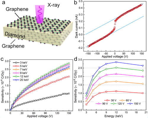
When exposed to high energy (hv) X-ray photons, excess electron-hole pairs will generate in the diamond bulk and then be separated by the applied electric field, and finally collected by graphene electrodes. The performance of the proposed GDG detector under X-ray radiation with different photon energies (3, 5, 7, 9, 12, and 20 keV) was investigated in dark at room temperature in the atmospheric environment. As shown in , the sensitivity of the detector depends on the applied voltage and incident X-ray energies. In the higher voltage region (60–150 V), the sensitivity of the device showed positive relation to the applied bias voltage. Meanwhile, according to , the sensitivity increased with the incident photon energy increasing and reached to a maximum value (2.88 × 10⁻⁸ C Gy−1 at 150 V) at 12 keV followed by a falling tendency with the incident photon energy keeping increasing, which is close to the result of 50–140 nC Gy−1 mm−3 for a commercial natural diamond-based X-ray detectors [Citation40]. The response of the GDG detector to X-rays indicates the possibility of fabricating diamond electronic devices with direct sp3-to-sp2 graphene layers as electrode materials.
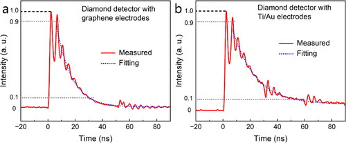
3.5. Comparison of the time response
The time response of the graphene-diamond-graphene detector was tested and compared to the diamond detector with Ti/Au electrode, as shown in . The X-ray source is Golden XRS-3, which emits two X-ray pulse at one time, the response of the diamond detector to X-ray is measured by an oscilloscope. When excited by 30 keV X-ray at 100 V bias, the two peaks of the double X-ray pulse can be clearly observed, indicating both the diamond detectors with graphene and Ti/Au electrodes have fast time response to X-rays. Detailly, the rise time of the GDG detector was as low as 1.2 ns, similar to that of diamond detector with Ti/Au (20/60 nm) electrodes (1.1 ns), as shown in . In term of the delay time, the value (∼ 22.8 ns) of GDG detector is lower than that of diamond detector with Ti/Au electrodes of ∼ 50 ns. The fast time response of the two diamond detectors was attributed to the high quality of the diamond. The diamond detectors with graphene and Ti/Au electrodes show similar time response to X-ray irradiations, indicating graphene can also be used as electrode materials as well as conventional metal electrodes.
Figure 5. Time response of diamond detectors with (a) graphene as electrodes and (b) Ti/Au as electrodes.
4. Conclusion
In this work, a graphene-diamond-graphene (GDG) detector was fabricated with Ni-catalytically conversed graphene layers as electrodes. Based on the direct sp3-to-sp2 conversion, the carbon-carbon bond on the diamond surface transfer from sp3- to sp2-hybridization with the assistance of Ni thin film. The layers of graphene can be limited into 2–3 layers with 15 nm-thick Ni film, under 1000 °C and 15 min treatment. Based on the first principles simulation, the direct formation of graphene on diamond surface has a strong interface interaction than CVD transferred graphene on H-diamond interface. The fabricated GDG detector shows a low dark current of 0.45 nA at 0.5 V μm−1, and a maximum response of 2.88 × 10⁻⁸ C Gy−1 at 0.5 V μm−1 at a 12 keV incident photons. Compared to conventional Ti/Au electrodes, the GDG detector shows a similar time response like detector using Ti/Au electrode. The one-step prepared all-carbon detector shows a high promise for the application of X-ray detectors and a potential method to fabricate carbon-based electronics. However, the difference of the the contact and interface between graphene and diamond need more investigation, together with the operation temperature and radiation toleration of using graphene as electrodes in diamond devices.
Supplemental Material
Download MS Word (763.2 KB)Disclosure statement
No potential conflict of interest was reported by the authors.
Additional information
Funding
Notes on contributors
Qilong Yuan
Qilong Yuan Postdoctoral fellow of Ningbo Institute of Materials Technology and Engineering (NIMTE), Chinese Academy of Sciences. Research interest: diamond related electronic and photonic devices.
Linyue Liu
Linyue Liu Research fellow of Northwest Institute of Nuclear Technology (NINT). Research interest: advanced neutron detection material, wide band-gap semiconductor detectors and radiation detection technology.
Dan Dai
Dan Dai Senior engineer of Ningbo Institute of Materials Technology and Engineering (NIMTE), Chinese Academy of Sciences. Research interest: electrochemical performance of diamond.
Yuhong Zhou
Yuhong Zhou Associate research fellow of Ningbo University of Technology. Research interest: DFT calculation on new materials and new structures.
Ying Liu
Ying Liu Master. Research interest: synthesis of carbon-based materials like diamond and graphene.
Mingyang Yang
Mingyang Yang Doctor student of Ningbo Institute of Materials Technology and Engineering (NIMTE), Chinese Academy of Sciences. Research interest: interface engineering on CVD diamond.
Mengting Qiu
Mengting Qiu Doctor student of Ningbo Institute of Materials Technology and Engineering (NIMTE), Chinese Academy of Sciences. Research interest: ultrawide bandgap photonic devices.
Zhenglin Jia
Zhenglin Jia Master student of Ningbo Institute of Materials Technology and Engineering (NIMTE), Chinese Academy of Sciences. Research interest: growth and interface engineering of diamond.
He Li
He Li Research fellow of Ningbo Institute of Materials Technology and Engineering (NIMTE), Chinese Academy of Sciences. Research interest: Synthesis and characterization of CVD diamond.
Kazhihito Nishimura
Kazhihito Nishimura Professor of Kogakuin University. Research interest: synthesis and processing of diamond.
Geng Tian
Geng Tian Research fellow of Northwest Institute of Nuclear Technology (NINT). Research interest: digital pulse processing in radiation detection.
Kuan W. A. Chee
Kuan W. A. Chee Professor of University of Science and Technology of China. Research interest: noval semiconductor materials and devices.
Shiyu Du
Shiyu Du Research fellow of Ningbo Institute of Materials Technology and Engineering (NIMTE), Chinese Academy of Sciences. Research interest: DFT calculation on new materials and new structures.
Cheng-Te Lin
Cheng-Te Lin Research fellow of Ningbo Institute of Materials Technology and Engineering (NIMTE), Chinese Academy of Sciences. Research interest: Structural manipulation and application of carbon-based materials.
Nan Jiang
Nan Jiang Research fellow of Ningbo Institute of Materials Technology and Engineering (NIMTE), Chinese Academy of Sciences. Research interest: carbon-based functional materials.
Xiaoping Ouyang
Xiaoping Ouyang Research fellow of Northwest Institute of Nuclear Technology (NINT). Research interest: advanced neutron detection material, wide band-gap semiconductor detectors and radiation detection technology.
References
- Tsao JY, Chowdhury S, Hollis MA, et al. Ultrawide-bandgap semiconductors: research opportunities and challenges. Adv Electron Mater. 2018;4(1):1600501.
- Donato N, Rouger N, Pernot J, et al. Diamond power devices: state of the art, modelling, figures of merit and future perspective. J Phys D Appl Phys. 2020;53(9):093001.
- Isberg J, Hammersberg J, Johansson E, et al. High carrier mobility in single-crystal plasma-deposited diamond. Science. 2002;297(5587):1670–1672.
- Kim M, Seo J-H, Singisetti U, et al. Recent advances in free-standing single crystalline wide band-gap semiconductors and their applications: GaN, SiC, ZnO, β-Ga2O3, and diamond. J Mater Chem C. 2017;5(33):8338–8354.
- Ren Z, Xing Y, Lv D, et al. Diamond MOS interface properties and FET characteristics with high-temperature ALD-grown HfO2 dielectric. AIP Adv. 2021;11(3):035041.
- Sato Y, Shimaoka T, Kaneko JH, et al. Radiation hardness of a single crystal CVD diamond detector for MeV energy protons. Nucl Instrum Methods Phys Res Sect A. 2015;784:147–150.
- Skukan N, Sudić I, Pomorski M, et al. Enhanced radiation hardness and signal recovery in thin diamond detectors. AIP Adv. 2019;9(2):025027.
- Koide Y, Liao M, Alvarez J. Thermally stable solar-blind diamond UV photodetector. Diamond Relat Mater. 2006;15(11–12):1962–1966.
- Oh A, Moll M, Wagner A, et al. Neutron irradiation studies with detector grade CVD diamond. Diamond Relat Mater. 2000;9:1987–1903.
- Wooldridge DE, Ahearn AJ, Burton JA. Conductivity pulses induced in diamond by alpha-particles. Phys Rev. 1947;71(12):913–913.
- Kozlov SF, Stuck R, Hage-Ali M, et al. Preparation and characteristics of natural diamond nuclear radiation detectors. IEEE Trans Nucl Sci. 1975;22(1):160–170.
- Bergonzo P, Brambilla A, Tromson D, et al. CVD diamond for radiation detection devices. Diamond Relat Mater. 2001;10(3–7):631–638.
- Bergonzo P, Brambilla A, Tromson D, et al. CVD diamond for nuclear detection applications. Nucl Instrum Methods Phys Res Sect A. 2002;476(3):694–700.
- Balducci A, Garino Y, Giudice AL, et al. Radiological X-ray dosimetry with single crystal CVD diamond detectors. Diamond Relat Mater. 2006;15(4–8):797–801.
- Morse J, Salomé M, Berdermann E, et al. Single crystal CVD diamond as an X-ray beam monitor. Diamond Relat Mater 2007;16(4–7):1049–1052.
- Kania DR, Landstrass MI, Plano MA, et al. Diamond radiation detectors. Diamond Relat Mater 1993;2(5–7):1012–1019.
- Balandin AA, Ghosh S, Bao W, et al. Superior thermal conductivity of single-layer graphene. Nano Lett. 2008;8(3):902–907.
- Chen JH, Jang C, Xiao S, et al. Intrinsic and extrinsic performance limits of graphene devices on SiO2. Nature Nanotech. 2008;3(4):206–209.
- Mathew S, Chan TK, Zhan D, et al. The effect of layer number and substrate on the stability of graphene under MeV proton beam irradiation. Carbon. 2011;49(5):1720–1726.
- Park H, Brown PR, Bulović V, et al. Graphene as transparent conducting electrodes in organic photovoltaics: studies in graphene morphology, hole transporting layers, and counter electrodes. Nano Lett. 2012;12(1):133–140.
- Jo G, Choe M, Lee S, et al. The application of graphene as electrodes in electrical and optical devices. Nanotechnology. 2012;23(11):112001.
- Yao K, Yang C, Zang X, et al. Carbon sp2-sp3 technology: graphene-on-diamond thin film UV detector. 2014 IEEE 27th International Conference on Micro Electro Mechanical Systems; (MEMS); 2014 Jan 26-30; San Francisco, CA, USA. IEEE; 2014.
- Wei M, Yao K, Liu Y, et al. A solar-blind UV detector based on graphene-microcrystalline diamond heterojunctions. Small. 2017;13(34):1701328.
- Jang H, Dai Z, Ha K-H, et al. Stretchability of PMMA-supported CVD graphene and of its electrical contacts. 2D Mater. 2019;7(1):014003.
- Loan PTK, Wu D, Ye C, et al. Hall effect biosensors with ultraclean graphene film for improved sensitivity of label-free DNA detection. Biosens. Bioelectron. 2018;99:85–91.
- Pallecchi E, Lafont F, Cavaliere V, et al. High electron mobility in epitaxial graphene on 4H-SiC(0001) via post-growth annealing under hydrogen. Sci Rep. 2014;4:4558.
- Tokuda N, Fukui M, Makino T, et al. Formation of graphene-on-diamond structure by graphitization of atomically flat diamond (111) surface. Jpn J Appl Phys. 2013;52(11R):110121.
- Ueda K, Aichi S, Asano H. Direct formation of graphene layers on diamond by high-temperature annealing with a cu catalyst. Diamond Relat Mater. 2016;63:148–152.
- Berman D, Deshmukh SA, Narayanan B, et al. Metal-induced rapid transformation of diamond into single and multilayer graphene on wafer scale. Nat Commun. 2016;7:12099.
- Kanada S, Nagai M, Ito S, et al. Fabrication of graphene on atomically flat diamond (111) surfaces using nickel as a catalyst. Diamond Relat Mater. 2017;75:105–109.
- Tulić S, Waitz T, Čaplovičová M, et al. Catalytic graphitization of single-crystal diamond. Carbon. 2021;185:300–313.
- Yuan Q, Liu Y, Ye C, et al. Highly stable and regenerative graphene–diamond hybrid electrochemical biosensor for fouling target dopamine detection. Biosens Bioelectron. 2018;111:117–123.
- Wu J, Xu H, Zhang J. Raman spectroscopy of graphene. Acta Chim Sin. 2014;72(3):301.
- Gu C, Li W, Xu J, et al. Graphene grown out of diamond. Appl Phys Lett. 2016;109(16):162105.
- Wu T, Liu Z, Chen G, et al. A study of the growth-time effect on graphene layer number based on a Cu–Ni bilayer catalyst system. RSC Adv. 2016;6(28):23956–23960.
- Hu W, Li Z, Yang J. Diamond as an inert substrate of graphene. J Chem Phys. 2013;138(5):054701.
- Selli D, Baburin I, Leoni S, et al. Theoretical investigation of the electronic structure and quantum transport in the graphene-C(111) diamond surface system. J Phys Condens Matter. 2013;25(43):435302.
- Talamonti C, Kanxheri K, Pallotta S, et al. Diamond detectors for radiotherapy X-ray small beam dosimetry. Front Phys. 2021;9:632299.
- Kono S, Teraji T, Takeuchi D, et al. Direct determination of the barrier height of Au ohmic-contact on a hydrogen-terminated diamond (001) surface. Diamond Relat Mater. 2017;73:182–189.
- Lansley SP, Betzel GT, Meyer J, et al. CVD diamond X-ray detectors for radiotherapy dosimetry. In IEEE SENSORS 2009 Conference, 2009 Oct 25–28; Christchurch, New Zealand. IEEE; 2009.