
 ?Mathematical formulae have been encoded as MathML and are displayed in this HTML version using MathJax in order to improve their display. Uncheck the box to turn MathJax off. This feature requires Javascript. Click on a formula to zoom.
Abstract
Sub-monolayers of titanium were deposited onto oxidised (100) single-crystal diamond surfaces and annealed in vacuo at temperatures up to 1000 °C to find a temperature-stable termination procedure that produces a surface with Negative Electron Affinity (NEA). The samples were analysed by X-ray Photoelectron Spectroscopy, Ultraviolet Photoelectron Spectroscopy and Energy-Filtered Photoemission Electron Microscopy to determine their electron affinity and work function values. NEA values were observed on samples following annealing above 400 °C, with the largest NEA value being –0.9 eV for a sample coated with a half-monolayer of Ti annealed at 400 °C. Work function values were ∼4.5 eV for all samples annealed at temperatures between 400 and 600 °C, then rose at higher temperatures due to the loss of substantial amounts of O from the surface. Work-function maps indicated that the surface was uniform over areas 5700 μm2, suggesting that the deposition and annealing steps used are reliable methods to produce films with homogeneous surface properties.
Graphical Abstract
1. Introduction
Diamond has many superlative properties and can be deposited as thin layers via Chemical Vapour Deposition (CVD) [Citation1]. These features, combined with its ability to form a negative electron affinity (NEA) surface, has made diamond a material of interest for numerous electron-emission applications [Citation2], such as photodiodes [Citation3], electron sources [Citation4], secondary-electron emission devices [Citation5], thermionic energy conversion [Citation6] and photoelectrochemical CO2 conversion [Citation7].
In order for an electron to be emitted from a metal surface, it must possess sufficient kinetic energy to overcome the work function (WF) situated at the surface–vacuum interface. The work function, ϕ, is defined as the energy difference between the Fermi level, EF, and that of the vacuum level. In semiconductors, electrons that reside in the valence band (VB) require additional energy equivalent to that of the band gap to first excite them into the conduction band (CB) before they can be emitted. ϕ typically has vales of a few eV for most metals and semiconductors. Therefore, high-energy ultraviolet photons or temperatures >1500 K are usually required to provide sufficient energy for electron emission. For some semiconductors and insulators, however, which include diamond [Citation8], cubic boron nitride [Citation9], and AlN and AlGaN [Citation10], the work function is greatly reduced because, in these unusual cases, the CB minimum lies higher in energy than the vacuum level. This condition is known as NEA. Here, electrons located in the CB experience no emission barrier to escape the surface. Bulk electrons residing in the VB, or in mid-band-gap states because of doping, only require prior excitation (via photon absorption, thermalisation or electric fields) into the CB for emission to take place. Consequently, NEA materials are highly desirable for next-generation electron-emission applications. Because these are all wide band-gap materials, the advantages of NEA might be outweighed by the high energies needed to excite electrons from the VB into the CB. However, this problem can be reduced if the NEA is sufficiently large and negative, i.e. has a value approaching that of the band gap, and also by using suitable doping strategies, especially n-type, that raise the Fermi level and decrease the effective band gap [Citation2].
In the case of diamond, an NEA surface can be formed by terminating the diamond surface with atoms or groups of atoms that are electropositive relative to that of bulk carbon, forming an electric dipole perpendicular to the surface, with positive charge outermost [Citation11]. Termination with hydrogen gives an NEA for each of the (100), (111) and (110) surfaces [Citation12–14]. However, H-terminated diamond surfaces suffer from hydrogen desorption at elevated temperatures (>∼700 °C) [Citation8,Citation15], which makes H-terminated diamond problematic for use in high-temperature applications, such as thermionic energy converters (TECs). Therefore, there is an extensive ongoing search for alternative diamond-termination schemes that provide high NEA whilst remaining stable above 1000 K [Citation2].
The H-terminated diamond surface can be functionalised by using a variety of wet chemistry and plasma techniques [Citation16] to produce surfaces with different terminations that exhibit improved emission behaviour and thermal stability. Previous experimental and computational studies of NEA surfaces on diamond include the use of Group I and II metals [Citation17–20] and transition metals (TMs) [Citation21–25] as the electropositive species, with monolayer (ML) or sub-monolayer coverage, on bare or oxidised diamond surfaces. Group I elements have long been known to exhibit NEA characteristics on diamond, however larger adsorbed Group I elements, such as Cs [Citation17], have low thermal stability which limits their usefulness at higher temperatures. Computational and experimental work has focused upon elements that can provide a robust surface alongside NEA, including smaller Group I and II metals, such as Li and Mg [Citation26–29] as well as various TMs like Cu, Ni, Ti and Zn [Citation24,Citation29].
Collective results from these studies suggest that for metals deposited directly onto the diamond surface, carbide-forming metals give a larger NEA. However, many metals do not readily form bonds with carbon, while others prefer bonding to oxygen over carbon, such that the adsorbed metal layer rapidly oxidises on exposure to air. Some of these problems can be overcome by depositing the metal onto an already oxidised diamond surface [Citation26]. While it may appear counterintuitive to terminate the surface with electronegative oxygen, provided a sufficiently electropositive metal (M) is bonded on top of the oxygen layer, the overall combination can produce a net NEA. An added benefit in these M–O–C systems is that the metal is already partially oxidised, lowering its reactivity towards further oxidation thereby making the surface more air stable.
These data sets suggest that for optimal NEA, together with an air- and temperature-stable diamond surface, it is preferable for the adsorbate to have the following attributes: (a) a high electropositivity, (b) a relatively small radius, (c) propensity to form highly charged positive ions, and (d) ready formation of bonds with both C and O.
With this in mind, our group recently reported the results of computational and/or theoretical studies for the metals Al [Citation30–33], Sn [Citation34,Citation35] and Sc [Citation36] on both bare and oxidised diamond surfaces. For Al, the Al–O–diamond surfaces remained stable up to 800 °C, with electron affinity (EA) values generally between 0.0 and –1.0 eV, and work functions 4.5–0.5 eV, depending upon the deposition method, coverage and annealing temperature [Citation33]. Quarter and half ML coverages of Sn were found to be the most stable coverages in the case of both bare and oxygen-terminated diamond, resulting in large adsorption energies (up to −6.5 eV on the oxygen-terminated surface with an EA up to −1.5 eV. For Sc on the oxygenated diamond (100) surface, simulations [Citation36] predicted extremely large adsorption energies (Ead) per adsorbate atom as high as −8.7 eV. Moreover, most of the stable Sc adsorption configurations were calculated to possess NEA, with the most negative values being –3.73 eV found for 0.25 ML Sc coverage. This study also predicted NEA and work function values for Sc on a nitrogenated diamond surface, showing that the M–N–diamond termination approach is also a potential route to temperature-stable NEA surfaces. Preliminary experimental results seem to be consistent with these predicted values [Citation37] for Sc termination. Other diamond terminations, such as Si, Ge, metal nitrides, amines and OH groups have also been studied, with varying degrees of success, all reviewed in Ref. [Citation2].
We now consider titanium as another likely NEA candidate due to its electropositive character (EN = 1.54), and its propensity to form highly charged cations (Ti2+, Ti3+, Ti4+) with relatively small ionic radii (0.5–1.0 Å depending upon coordination number and ionic charge) [Citation38]. Moreover, Ti reacts readily with C, O and N, and is chemically similar to Al and Sc.
In this paper, we report experimental results from the Ti–O–diamond system, including measurements of work function and EA from different diamond surfaces, and coverages, as part of the quest to identify a diamond surface with a high electron-emission yield at low temperatures (∼500 °C), that will not degrade during use, and which will be compatible with commercial TECs for solar power applications.
2. Method
Single-crystal diamond substrates were purchased from Element Six, Ltd (Ascot, UK). These square undoped (100) substrates were made using chemical vapour deposition (CVD) with a surface polished to an average roughness of ∼3.9 nm and a side-length of 3 mm. To remove contamination following the polishing process, these samples were refluxed in a solution of potassium nitrate (5 g) in concentrated sulfuric acid (100 ml) for 6 h, then washed with deionised water [Citation39]. An electrically conducting boron-doped diamond (BDD) overlayer (∼1 µm) was grown homoepitaxially on these substrates using hot-filament CVD following the procedure described in Ref. [Citation33]. This BDD layer was needed to make the surface conductive and prevent surface-charging effects during characterisation procedures that rely on electron emission from the sample, such as X-ray Photoelectron Spectroscopy (XPS).
To ensure all samples started out with identical fully hydrogenated surfaces, the cleaned BDD-coated diamond substrates were placed into a microwave CVD reactor and a hydrogen plasma was used to hydrogenate the surface in a multi-step process, as described in Ref. [Citation40].
To convert the H-terminated diamond samples into O-termination, they were placed into a bespoke parallel-plate D.C. plasma reactor and exposed to an O2 plasma at room temperature (20 °C). The base pressure of the system was <5 mtorr while the operating pressure was typically 1 torr at an O2 (99.995%) flow rate of 10 sccm. The sample treatment time was only 7 s, which had been determined by previous calibration experiments to be the optimal duration—sufficient to fully oxygen terminate the surface without etching the diamond.
XPS analysis of the O2-plasma-treated samples determined that 5.7 ± 0.1% content was equivalent to 1 ML of O on the diamond surface. The average work function of these oxidised samples determined from ultraviolet photoelectron spectroscopy (UPS) plots (see ) was 5.4 ± 0.15 eV, which, while slightly higher than literature values, was in close agreement with the values obtained from the work–function maps of these samples (see later). Detailed analysis of the XPS peaks for O showed that these oxidised surfaces had 70–80% of the O in the bridging ether (C–O–C) configuration with the balance in the ketone (C = O) configuration [Citation39].
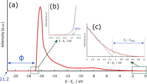
Figure 1. (a) Example UPS spectrum taken from a quarter monolayer of Ti on oxidised diamond, showing the additional large secondary-electron emission peak component at ∼16 eV indicative of NEA. Following convention, the plot begins at 21.2 eV, the photon energy of the He–I UV light source, and ends at the Fermi level, EF = 0. (b) Inset illustrating how the secondary electron cut-off (SECO) is obtained by extrapolation of the linear part of the plot to the axis. Thus, ϕ is given by 21.2 – SECO. (c) Inset illustrating how EVBM is obtained from linear extrapolation of the plot.
Ti was deposited in situ in the fabrication chamber of the University of Bristol NanoESCA II Facility under ultra-high vacuum (UHV) conditions. This was achieved using a four-pocket thin-film electron-beam evaporator. A high-purity (99.99%) Ti rod was used as the Ti source, and its evaporation rate was calibrated using a quartz microbalance and monitored using XPS [Citation39]. Thus, different evaporation times allowed deposition of fractions of a ML of Ti, as required. The deposition was performed at 400 °C. This was followed by an in situ UHV anneal at temperatures 600–1000 °C. The anneal created a strong covalent bond between the surface atoms (O or C) and any adjacent overlying Ti atoms, while any excess, unbonded metal or oxygen, thermally desorbed and was pumped away. UPS was also performed in a separate chamber in the NanoESCA system. Thus, sequential deposition, annealing and XPS/UPS analysis steps were possible without breaking vacuum.
XPS was used to obtain the elemental composition of the first few atomic layers of the samples. The relative amounts of each element, and their atomic percentage coverage were determined via calibration using the peak area for each element and its sensitivity factor (available from XPS literature [Citation41]). A monochromatic Al Kα X-ray source (1486.7 eV) was used with an overall energy resolution of 600 meV at a pass energy of 20 eV. The XPS binding-energy scale was calibrated by aligning the Au 4f7/2 peak to 84.0 eV using a polycrystalline gold film.
UPS was used to study the VB electrons in a sample. A UPS spectrum typically shows a large peak at high binding energy due to secondary-electron emission. Other peaks give information on the electron density-of-states. NEA can be observed by the presence of an extra secondary-electron emission peak component at a higher binding energy, arising from the additional secondary-electron population exceeding the vacuum energy [Citation40], as shown in . The work function, ϕ, can be calculated from the difference between the photon energy and the emission onset for PEA surfaces (). However, for NEA surfaces this method can be inaccurate. Instead, all work-function values were obtained directly from two-dimensional maps measured using Energy-Filtered Photoemission Electron Microscopy (EF-PEEM), as described below. UPS was also used to determine the difference between EF and the energy of the VB maximum, EVBM. Thus, the EA, χ, was calculated from:
(1)
(1)
where Eg is the band gap of diamond (5.45 eV).
Region-selected UPS was performed using EF-PEEM with a monochromatised He–I light source (21.2 eV) in the NanoESCA II system. Photoemitted electrons were filtered by kinetic energy in the first hemisphere of an imaging double-hemisphere energy analyser, and the signal was amplified using a channeltron. The energy resolution of this technique was 0.14 eV. An iris allowed UPS to be performed on a region of interest of ∼200 μm2.
EF-PEEM was also used to extract a map of the work function across a sample surface. As in UPS, photo-emitted electrons were energy filtered using an imaging double-hemisphere energy analyser. For EF-PEEM, images were obtained for successive energies, allowing the work function at different locations to be visualised as a colour-coded map, with an energy resolution of 0.15 eV and a spatial resolution of ∼150 nm. The UV-light source was the same monochromatic He–I lamp used for UPS. Photoelectrons were extracted from the sample by applying a bias of 7–12 kV across the sample-to-extractor-electrode distance of ∼1.8 mm. The work-function values were then corrected for the Schottky effect of 98 meV resulting from the high PEEM extractor field [Citation42], directly producing values of ϕ with an uncertainty of about ±0.15 eV.
3. Results
Samples of Ti on oxidised diamond were prepared with different thicknesses of Ti corresponding to a quarter monolayer (QML), half ML (HML) and full ML (FML), and their work function, EA and surface composition were analysed as a function of annealing conditions.
Composition changes following annealing
The Ti XPS survey spectrum from the as-deposited (400 °C) QML sample is shown in Figure S1 in the Supplementary Information. Figure S2 in the Supplementary Information is an expansion of this spectrum around the Ti 2p region, showing a large component at 458.5 eV (81.5%) and a smaller component at 457.4 eV (18.5%), both of which correspond to TiO. If the deposition were non-uniform, i.e. island growth, the Ti 2p spectrum would also exhibit a metallic component around 454 eV and there would be an increase in the O concentration due to the Ti in the islands oxidising. Because neither of these are seen, this suggests the Ti has formed a uniform coherent layer bonded to the oxidised surface.
shows the elemental composition of the surface following a series of 15-min anneals at successively higher temperatures. For the QML sample, after annealing at 600 °C for 15 min there was a small decrease in the O concentration while the Ti concentration remained largely unchanged. However, after annealing the sample at 800 °C, there was significantly less O remaining relative to the full ML before Ti deposition. There was also a 0.3% decrease in the concentration of Ti. However, considering that no corresponding decrease in Ti concentration was observed after the 1000 °C anneal, and that an increase in temperature would typically result in more of the species desorbing, it is unlikely that this decrease is due to Ti desorption. The decrease in Ti concentration could be due to the Ti atoms on the surface rearranging or diffusing into the bulk of the diamond. Following the 1000 °C anneal, most of the O had desorbed, although the O 1s core-level scan revealed that there were trace amounts of O remaining. These trends are replicated for the HML and FML samples: above ∼800 °C O desorption becomes significant, and nearly all O has disappeared from the surface by 1000 °C, while the Ti concentration appears largely unchanged at all temperatures.
Table 1. Elemental surface composition derived from XPS for 3 different Ti coverages following oxidation at 20 °C, Ti deposition at 400 °C, and then following annealing at 3 higher temperatures (15 min each).
Bonding changes following annealing
shows the percentage by area of the surface (a) oxygen or (b) carbon atoms that are bonded in different ways after annealing at different temperatures for QML Ti deposition, following analysis of the deconvoluted components of the core level XPS spectra. Examples of the fitting and deconvolution process for the XPS spectra are given in Figures S3 and S4 in the Supplementary Information. In , before Ti deposition (20 °C) the oxygen components are typical of those observed for O-terminated diamond, with a large (76%) ether component at 532.3 eV and a smaller (23%) ketone component at 531.1 eV. There is also a trace metal oxide peak at 529.7 eV probably due to slight Ti contamination in the XPS chamber. After Ti deposition at 400 °C, it can be seen immediately that the metal–oxide component has increased significantly and is now the largest component (∼36%). This is to be expected after depositing Ti on the O-terminated surface and shows that the Ti has chemically bonded to the O, rather than being physically adsorbed on the surface. After the 600 °C anneal, peak composition shifts even more towards the metal–oxide component, and even further following the 800 °C anneal.
Figure 2. Percentage of the surface (a) O or (b) C atoms by area that are involved in different bonding arrangements after annealing at different temperatures for QML Ti deposition, obtained by analysis of the deconvoluted components of the core level XPS spectra. (a) Analysis of the O 1s peaks determines the O bonding in terms of ether (533 eV), ketone (532 eV), and metal oxide (531 eV) composition. (b) Analysis of the C 1s peaks determines the C bonding in terms of oxidation level (ether 288 eV and ketone 287 eV), C–C bonds (sp2 285 eV and sp3 284 eV) and two different metal–carbide bonds (283 eV and 282 eV).
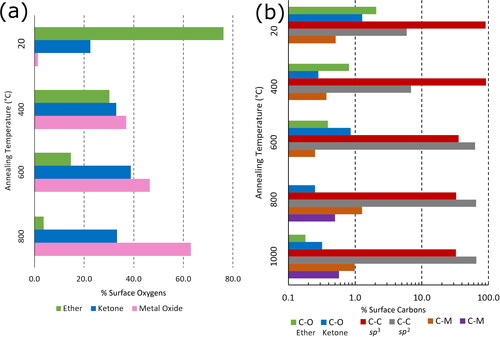
shows a bar chart for the component ratios of surface C atoms. This is displayed on a logarithmic scale because a linear scale would only show the two large C–C components from the diamond substrate. The chart clearly shows the C–O components at ∼288 eV decreasing in magnitude with increasing temperatures while the metal–carbide peaks ∼282 eV increase in magnitude. One interesting aspect is that the second metal–carbide component (purple bar in ) could only be observed after most of the O had desorbed at T > 800 °C. It is also worth noting that the sp3 C–C peak dominates at low temperature, as expected for single-crystal diamond, but after Ti deposition and annealing, the sp2 peak height increases and even exceeds that of the sp3 peak. This may reflect the change in hybridisation of the surface C atoms when they are partially bonded to a Ti atom. The nature of the bonding of Ti to the C and O atoms on the surface would make an excellent topic for future theoretical studies.
EA and WF
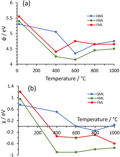
UPS and EF-PEEM analysis were performed on the QML, HML and FML samples before and after Ti deposition, as well as following the anneals. The EA and WF values after these anneals are summarised in . At 20° C, before Ti deposition, the work–function values of all three samples were relatively high (5.3–5.5 eV) and they all exhibited PEA with values 0.7–1.2 eV, consistent with O-terminated diamond. After Ti deposition at 400 °C, the WF and EA values of all three samples decreased markedly, although the values for the QML sample decreased significantly less than the other two. Indeed, at this temperature the HML and FML samples exhibited quite significant NEA values of –0.9 and –0.3 eV, respectively. With further increases in temperature, the EA values for each of the three coverages remained roughly constant, while the work–function values gradually climbed back to a value around 4.5 eV. This increase in work function can be correlated with the loss of oxygen at these higher temperatures (see Figure S5 in the Supplementary Information).
Figure 3. Variation with annealing temperature of (a) the work function, and (b) the electron affinity for the TiO-terminated diamond samples. The uncertainty in both ϕ and χ data values is ±0.15 eV.
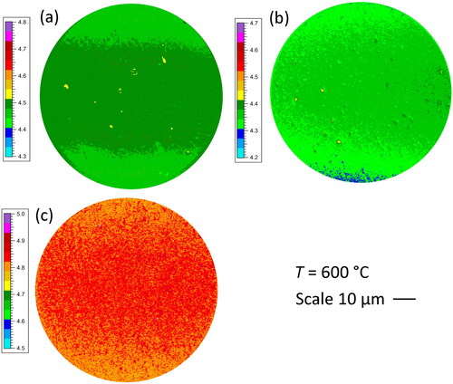
The optimum temperature for annealing is ∼600 °C, which is sufficient to restructure the surface and chemically bond the Ti, O and C together, producing high NEA values and low work functions, without causing significant desorption of O. WF maps of the samples annealed at 600 °C are given in . These show that apart from a few submicron blemishes, the majority of the surface exhibits a reasonably uniform WF to within about ±0.05 eV over an area with a diameter ∼85 μm (∼5700 μm2).
Figure 4. Work–function maps obtained by EF-PEEM for (a) QML, (b) HML, and (c) FML of Ti on oxidised diamond annealed at 600 °C.
4. Discussion
For anneals at temperatures >400 °C, the HML and FML Ti coverages exhibited EA values ∼ –0.3 eV and ∼ –0.8 eV, respectively. WF values dropped from ∼5.5 eV for oxidised diamond to ∼4.5 eV as annealing temperatures increased to 600 °C, then rose again at higher temperatures. In general, these results are broadly consistent with computational predictions [Citation39], although the recent predictions of Tiwari et al. [Citation25] calculate PEA values for all Ti–O–diamond configurations except the FML coverage, which is predicted to have a rather large NEA of –3.1 eV. Care should be taken with these comparisons, however, as the simulations were for undoped diamond whereas the experimental substrates had a conducting BDD layer to facilitate XPS analysis. As well as changing the electrical conductivity of the bulk, dopants also produce band bending at the surface, and this can have a significant effect upon the magnitude and sign of the measured EA [Citation43]. Tiwali et al.’s calculations do predict a very high adsorption energy for Ti on oxidised diamond of ∼7 eV, which is consistent with our experiment which showed no significant loss of Ti, even at 1000 °C annealing.
Our experimental values of EA and WF also compare favourably with those reported for surface terminations with elements similar to Ti. For Al–O termination, the EA values were between 0.0 and –1.0 eV, with WFs 4.5–0.5 eV, depending upon the deposition method, coverage and annealing temperature [Citation33]. For Sn–O termination, NEA values of −0.86 eV and −1.37 eV were obtained with QML and HML of Sn, respectively, on oxygen-terminated (100) diamond [Citation35], with corresponding WFs of 3.9 and 4.1 eV. These EA and WF values are slightly better than the values for TiO, however, these SnO terminations desorbed above 700–800 °C making their use in thermionics problematic. For ScO termination, nearly all of the stable Sc adsorption configurations were calculated [Citation35] and measured [Citation37] to possess NEA, with the largest value being –3.73 eV found for QML coverage. The corresponding work functions were in the range 1.4–4.0 eV. The EA values are significantly larger than those for Ti measured in this work, while the WF values are much smaller. Thus, comparing these four terminations options, ScO looks the most promising with large NEA values and small WFs, with TiO and AlO jointly vying for second place, and SnO last due to its low desorption temperature. Although Sc appears to be the better choice, one advantage that both Al and Ti have over Sc is that they are both common, inexpensive metals compared to Sc, and in device fabrication, sometimes low production cost is more important than absolute performance.
The main issue with the Ti–O-termination was the change in oxygen behaviour with temperature rather than desorption of Ti. At higher temperatures, as much as 90% of the O coverage was lost. This was unexpected because O-terminated diamond is usually stable to ∼900 °C [Citation14,Citation44] and TiO2 to >1800 °C. Preliminary results suggest this loss of O may be related to a restructuring of the surface at certain coverages, such that some or all of the O atoms migrate to the surface. This is still under investigation, but it means that careful control of annealing temperatures is required to ensure the temperature is sufficient to chemically bond the C, O and Ti to activate NEA, but not high enough to promote significant loss of O.
From the XPS results, one of the key issues here is the difficulty of forming a uniform O-terminated surface where the oxygens are all in either the ketone or ether bridging positions. Optimisation of an oxidation process that preferentially produces only one type of oxygenated diamond surface, such as that reported by Yoshida et al. [Citation45], would be a key goal to improve uniformity.
The time dependence of the EA and WFs of these films have yet to be studied. In order to produce usable thermionic devices, the surfaces must retain their NEA properties for service periods of years withstanding continual thermal cycling, and in common with many other diamond terminations, these long-term stability measurements have yet to be determined for TiO–diamond.
Finally, it is worth mentioning that, in parallel with these experiments involving Ti deposition onto O-terminated diamond, we performed similar experiments using N-terminated diamond [Citation39]. The N-termination was attempted using a NH3 plasma, however preliminary XPS results showed that the surface was contaminated with Fe and Cr from the plasma-reactor walls, which had been etched and redeposited onto the sample by the reactive NH3 plasma. The surface also had contamination from F and O, presumably due to the same source. As a result, the NEA and work function results were patchy and unreliable. Nevertheless, depositing metals onto a nitrogenated diamond surface is a viable and promising route to NEA surfaces that remains to be properly studied.
5. Conclusions
Ti was deposited onto O-terminated diamond, with the intention of producing a thermally stable surface with low work function and NEA. NEAs were observed following anneals at >400 °C, with the largest NEA value being –0.9 eV for the HML sample annealed at 400 °C. WF values dropped from those expected for oxidised diamond (∼5.5 eV) to ∼4.5 eV as annealing temperatures increased to 600 °C, then rose again at higher temperatures, due to the loss of substantial amounts of O from the surface via desorption, as evidenced by XPS composition analysis. WF maps indicated that the surface was uniform over areas with diameter 85 μm, suggesting that the deposition and annealing steps used are reliable methods to produce films with homogeneous surface properties. The WF and EA values are consistent with those measured previously by our group using a thick-film deposition method [Citation46]. Although the EA and work function values for these TiO–diamond surfaces are not as useful as those from the recently reported ScO–diamond system, the results show that TiO–diamond can still make an effective surface for thermionic devices which may be cheaper to fabricate that those made using Sc.
Acknowledgements
FF thanks the Engineering and Physical Sciences Research Council (EPSRC) for funding (EP/L015315/1) as part of the Diamond Science & Technology, Centre for Doctoral Training. The authors acknowledge the Bristol NanoESCA Facility (funded by EPSRC Strategic Equipment Grants EP/K035746/1 and EP/M000605/1).
Disclosure statement
The authors report there are no competing interests to declare.
Additional information
Funding
Notes on contributors
Fabian Fogarty
Fabian Fogerty studied for his PhD in the CVD diamond group of the University of Bristol from 2019 to 2021, as part of the Centre for Doctoral Training in Diamond Science & Technology funded by the UK EPSRC. His PhD thesis studied electron emission from Ti-terminated diamond surfaces, using experimental methods alongside DFT computational simulations. He is now a cybersecurity manager for a major international telecommunications company.
Neil A. Fox
Neil Fox is a Professor in Materials for Energy in the University of Bristol CVD Diamond Group and Head of the Diamond New Energy Group. In the last 15 years he has filed 18 patents on electron and plasma devices and published 50 peer-reviewed papers. He was a part of the Corporate Research Department at Smiths Industries Aerospace for 15 years until 2001. During 1995–1998, he was awarded an 1851 Royal Commission Industrial Fellowship and seconded to the University of Bristol Physics Department, where he subsequently became a member of staff. Since 2013 he has been awarded £3M of EPSRC funding for research projects associated with new diamond technology focused on energy generation and storage.
Paul W. May
Paul May was promoted to Professor in the School of Chemistry at Bristol University (UK) in 2010. He held a Ramsay Memorial Fellowship (1992–1994) and a Royal Society University Research Fellowship (1994–1999). He co-founded the Bristol CVD diamond group in 1991, which is now one of leading groups for diamond growth and research in the world. He has published over 250 papers/articles in refereed Journals, 200+ of which are on the subject of diamond/DLC films, and has given invited and contributed talks at more than 50 international conferences.
References
- May PW. Diamond thin films: a 21st century material. Phil Trans R Soc Lond A. 2000;358(1766):473–495.
- James MC, Fogarty F, Zulkharnay R, et al. A review of surface functionalisation of diamond for thermionic emission applications. Carbon. 2021;171:532–550.
- Monroy E, Omnés F, Calle F. Wide-Bandgap semiconductor ultraviolet photodetectors. Semicond Sci Technol. 2003;18(4):R33–R51.
- Ascarelli P, Cappelli E, Pinzari F, et al. Secondary electron emission from diamond: physical modeling and application to scanning electron microscopy. J Appl Phys. 2001;89(1):689–696.
- Shih A, Yater J, Pehrsson P, et al. Secondary electron emission from diamond surfaces. J Appl Phys. 1997;82(4):1860–1867.
- Koeck FAM, Nemanich RJ, Lazea A, et al. Thermionic electron emission from low work-function phosphorus doped diamond films. Diamond Relat Mater. 2009;18(5–8):789–791.
- Hamers RJ, Bandy JA, Zhu D, et al. Photoemission from diamond films and substrates into water: dynamics of solvated electrons and implications for diamond photoelectrochemistry. Faraday Discuss. 2014;172:397–411.
- Diederich L, Küttel OM, Aebi P, et al. Electron affinity and work function of differently oriented and doped diamond surfaces determined by photoelectron spectroscopy. Surf Sci. 1998;418(1):219–239.
- Loh KP, Sakaguchi I, Nishitani-Gamo M, et al. Negative electron affinity of cubic boron nitride. Diamond Relat Mater. 1999;8(2-5):781–784.
- Nemanich RJ, Baumann PK, Benjamin MC, et al. Negative electron affinity surfaces of aluminum nitride and diamond. Diamond Relat Mater. 1996;5(6-8):790–796.
- Cui JB, Ristein J, Ley L. Electron affinity of the bare and hydrogen covered single crystal diamond (111) surface. Phys Rev Lett. 1998;81(2):429–432.
- Van Der Weide J, Zhang Z, Baumann PK, et al. Negative-electron-affinity effects on the diamond (100) surface. Phys Rev B. 1994;50(8):5803–5806.
- Himpsel FJ, Knapp JA, VanVechten JA, et al. Quantum photoyield of diamond(111)—a stable Negative-Affinity emitter. Phys Rev B. 1979;20(2):624–627.
- Baumann PK, Nemanich RJ. Surface cleaning, electronic states and electron affinity of diamond (100), (111) and (110) surfaces. Surf Sci. 1998;409(2):320–335.
- Paxton WF, Howell M, Kang WP, et al. Influence of hydrogen on the thermionic electron emission from nitrogen-incorporated polycrystalline diamond films. J Vac Sci Technol B. 2012;30(2):021202.
- Raymakers J, Haenen K, Maes W. Diamond surface functionalization: from gemstone to photoelectrochemical applications. J Mater Chem C. 2019;7(33):10134–10165.
- Loh KP, Foord JS, Egdell RG, et al. Tuning the electron affinity of CVD diamond with adsorbed caesium and oxygen layers. Diam Relat Mater. 1997;6(5-7):874–878.
- Loh KP, Xie XN, Yang SW, et al. A spectroscopic study of the negative electron affinity of cesium Oxide-Coated diamond (111) and theoretical calculation of the surface density-of-States on oxygenated diamond (111). Diamond Relat Mater. 2002;11(7):1379–1384.
- Wong KW, Wang YM, Lee ST, et al. Lowering of work function induced by deposition of ultra-thin rubidium fluoride layer on polycrystalline diamond surface. Appl Surf Sci. 1999;140(1–2):144–149.
- Nie JL, Xiao HY, Zu XT, et al. First principles calculations on Na and K-adsorbed diamond (100) surface. Chem Phys. 2006;326(2–3):308–314.
- Baumann PK, Nemanich RJ. Characterization of cobalt-diamond (100) interfaces: electron affinity and schottky barrier. Appl Surf Sci. 1996;104–105:267–273.
- Baumann PK, Nemanich RJ. Electron affinity and schottky barrier height of metal–diamond (100), (111), and (110) interfaces. J Appl Phys. 1998;83(4):2072–2082.
- van der Weide J, Nemanich RJ. Schottky barrier height and negative electron affinity of titanium on (111) diamond. J Vac Sci Technol B. 1992;10(4):1940–1943.
- Tiwari AK, Goss JP, Briddon PR, et al. Effect of different surface coverages of transition metals on the electronic and structural properties of diamond. Phys Status Solidi A. 2012;209(9):1697–1702.
- Tiwari AK, Goss JP, Briddon PR, et al. Unexpected change in the electron affinity of diamond caused by the ultra-thin transition metal oxide films. EPL. 2014;108(4):46005.
- O’Donnell KM, Martin TL, Fox NA, et al. Ab initio investigation of lithium on the diamond C(100) surface. Phys Rev B. 2010;82(11) 115303.
- O’Donnell KM, Martin TL, Allan NL. Light metals on oxygen-terminated diamond (100): structure and electronic properties. Chem Mater. 2015;27(4):1306–1315.
- O’Donnell KM, Martin TL, Edmonds MT, et al. Photoelectron emission from lithiated diamond. Phys Status Solidi A. 2014;211(10):2209–2222.
- O’Donnell KM, Edmonds MT, Tadich A, et al. Extremely high negative electron affinity of diamond via magnesium adsorption. Phys Rev B. 2015;92(3):35303.
- James KM. Aluminium and oxygen termination of diamond for thermionic applications [PhD thesis]. University of Bristol, UK; 2019. Available from: http://www.chm.bris.ac.uk/pt/diamond/michael-james-thesis/Michael-James-thesis.pdf.
- James MC, Croot A, May PW, et al. Negative electron affinity from aluminium on the diamond (100) surface: a theoretical study. J Phys Condens Matter. 2018;30(23):235002.
- James MC, May PW, Allan NL. Ab initio study of negative electron affinity from light metals on the oxygen-terminated diamond (111) surface. J Phys Condens Matter. 2019;31(29):295002.
- James MC, Cattelan M, Fox NA, Sila RF, Silva M, May PW. Experimental studies of electron affinity and work function from aluminium on oxidised diamond (100) and (111) surfaces. Phys Status Solidi B Basic Solid State Phys. 2021;258:2100027.
- Ullah S, Fox NA. Modification of the surface structure and electronic properties of diamond (100) with tin as a surface termination: a density functional theory study. J Phys Chem C. 2021;125(45):25165–25174.
- Ullah S, Wan G, Kouzios C, et al. Structure and electronic properties of tin monoxide (SnO) and lithiated SnO terminated diamond (100) and its comparison with lithium oxide terminated diamond. Appl Surf Sci. 2021;559:149962.
- Zulkharnay R, Allan NL, May PW. Ab initio study of negative electron affinity on the scandium-terminated diamond (100) surface for electron emission devices. Carbon. 2022;196:176–185.
- Zulkharnay R, May PW. in preparation. 2022.
- WebElements: Titanium: radii of atoms and ions. Available from: https://www.webelements.com/titanium/atom_sizes.html.
- Fogarty F. Renewable energy – low temperature thermionic emission from modified diamond surfaces [PhD thesis]. University of Bristol, UK; July 2020.
- Wan G, Cattelan M, Fox NA. Electronic structure tunability of diamonds by surface functionalization. J Phys Chem C. 2019;123(7):4168–4177.
- Yeh JJ, Lindau I. Atomic calculation of photoionization Cross-Sections and asymmetry parameters. Langhorne (PA): Gordon and Breach; 1993.
- Wan G, Panditharatne S, Fox NA, et al. Graphene–diamond junction photoemission microscopy and electronic interactions. Nano Express. 2020;1(2):020011.
- Larsson K. The combined influence of dopant species and surface termination on the electronic properties of diamond surfaces. J Carbon. 2020;6(2):22.
- Loh KP, Xie XN, Yang SW, et al. Oxygen adsorption on (111)-oriented diamond: a study with ultraviolet photoelectron spectroscopy, temperature-programmed desorption, and periodic density functional theory. J Phys Chem B. 2002;106(20):5230–5240.
- Yoshida R, Miyata D, Makino T, et al. Formation of atomically flat hydroxyl-terminated diamond (111) surfaces via water vapor annealing. Appl Surf Sci. 2018;458:222–225.
- Othman MZ. Studies of n-type doping and surface modification of CVD diamond for use in thermionic applications [PhD thesis]. University of Bristol, UK; 2014.