
 ?Mathematical formulae have been encoded as MathML and are displayed in this HTML version using MathJax in order to improve their display. Uncheck the box to turn MathJax off. This feature requires Javascript. Click on a formula to zoom.
Abstract
The response property and stability of diamond Schottky barrier photodiodes (SBPDs) were investigated for the monitor applications of deep ultraviolet (DUV) light and high-energy radiation particles. The SBPDs were fabricated on the unintentionally doped insulating diamond epilayer grown on a heavily boron-doped p+-diamond (100) conductive substrate by microwave plasma chemical vapor deposition. The vertical-type SBPDs were constructed of semitransparent tungsten carbide (WC) Schottky contact on the top of the device and a WC/titanium ohmic contact on the bottom. The SBPDs were operated to detect the DUV light and protons in zero-bias photovoltaic mode. The spectral response of the SBPDs showed that the peak wavelength was at 182 nm with a sensitivity of 46 ± 1 mA/W. The response speed was shorter than 1 sec, with a negligible charge-up effect and persistent photoconductivity. The SBPDs showed a stable response upon the irradiation by 172-nm xenon excimer lamp with 70 mW/cm2 for 200 hrs and 70 MeV protons for the dose of 10 MGy, corresponding to a non-ionizing energy loss of 1.4 × 10¹⁶ MeV neq/cm2.
1. Introduction
Diamond is a promising semiconductor for detecting deep ultra-violet (DUV) light and high-energy charged particles. A marked improvement in the detection performance is expected from its excellent physical properties, such as large bandgap energy of ∼5.5 eV [Citation1], high radiation resistance, the highest thermal conductivity of 22 W/cm·K, and high thermal stability. The advanced semiconductor integrated circuits require high-resolution photolithography with a shorter wavelength than 193 nm. The DUV-light monitors are needed to calibrate the output power of the light source for the photolithography. On the other hand, radiation monitors are indispensable for high-energy and high-flux radiation places, such as nuclear reactors, accelerators, and cosmic space. In the early development of diamond detectors, the research interest was placed on using poly-crystalline diamonds[Citation1–5]. Later, the research on diamond detectors was carried out using single-crystalline diamonds owing to the great progress in developing device-grade epilayers by a microwave plasma chemical vapor deposition (MPCVD) technique [Citation6–11]. Recently, high-performance solar-blind UV photodetectors have been reported based on the heterojunction of graphene/diamond [Citation12] or β-Ga2O3/diamond [Citation13]. The research and development team for diamond radiation detectors (RD42), collaborating with many institutes and universities, has long investigated diamond detectors for radiation monitoring and tracking [Citation14–16].
The excellent photoresponse properties of single-crystalline diamond DUV detectors were revealed within a series of our work [Citation17]. The configuration of the photodetectors was planar-type, fabricated on unintentionally-doped epilayers grown on Ib-type nitrogen-doped insulating diamond (100) substrates by MPCVD [Citation18]. The semitransparent tungsten carbide (WC) and annealed WC/titanium (Ti) metals were used as the Schottky and ohmic electrodes, respectively. The thermally stable operation and solar-blind property were obtained owing to the use of a homoepitaxially grown diamond layer and WC metals [Citation19, Citation20]. In particular, the combination of hard materials between diamond and WC was a critical factor in providing excellent thermal stability. One of the unique properties was that the photodetectors exhibited a huge photoconductivity gain, which is substantially larger than unity, producing an enormous photocurrent [Citation21]. However, the colossal photocurrent was accompanied by a persistent electrical conductivity, which induced a slow response speed [Citation22]. One reason was the existence of nitrogen in the substrate, which might act as a deep trap and lead to space charge separation. In addition, the charge-up problem came up under the high-flux irradiation of UV light due to the use of an insulating substrate.
The vertical-type Schottky barrier photodiodes (SBPDs) using single-crystalline diamond were developed as the next step to overcome these problems [Citation23]. The SBPDs were fabricated on the unintentionally-doped epilayer grown on a heavily boron-doped p+-diamond (100) conductive substrate by MPCVD. The semitransparent WC and WC/Ti metals were formed at the top and bottom, respectively. The SBPDs did not provide the photoconductivity gain property and persistent photocurrent due to the reduction of nitrogen [Citation24]. Although the typical photoresponse property from UV and visible light region (220 to 640 nm) has been reported, the stability under high-flux DUV light and radiation has not yet been explored.
This study investigates the response property in DUV region and the stability of diamond-based vertical-type SBPDs upon the radiation by a 172-nm xenon excimer lamp with a power density of 70 mW/cm2 and a high-energy 70 MeV protons. The appropriate device operation mode for the monitors is discussed based on these results.
2. Experimental
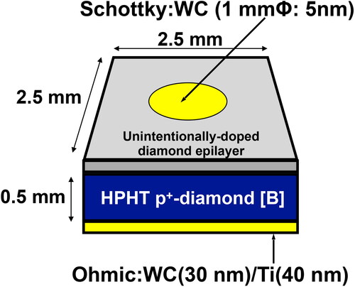
The unintentionally-doped diamond epilayers with a thickness of 0.5 or 1.6 μm were homoepitaxially grown on p+-diamond (100) substrate by MPCVD system (CORNES Technologies, AX5200S). The p+-diamonds with 2.5 × 2.5 × 0.5 mm3 in size were used as the substrate from Technological Institute for Super-hard and Novel Carbon Materials (TISNCM). The nominal boron concentration of the p+-diamond substrate was ∼1020 cm−3. The resistivity, hole carrier concentration, and hole mobility evaluated by Hall-effect measurement were 0.5 ± 0.2 Ωcm, 8.7 × 10¹⁸–1.2 × 1019 cm−3, and 3 ± 1.5 cm2/Vs, respectively. The hole mobility decreased with increasing the boron concentration [Citation25]. The source gases are H2 and CH4 for the diamond growth. The ratio of CH4 and H2 was 0.05%, and the corresponding flow rates of CH4 and H2 were 0.5 and 500 sccm, respectively. The reactor pressure and growth temperatures were 80 Torr and 800-850 °C, respectively. The boron concentration of the epilayer was controlled at ∼1015 cm−3 or less [Citation26]. Prior to fabricating the SBPD, the samples were oxidized for 1 hr in a boiling acid solution of H2SO4/HNO3 (1:1). The semitransparent WC (5 nm, 1 mmΦ) and WC (30 nm)/Ti (40 nm) electrodes were deposited for the formation of Schottky and ohmic contacts by sputter deposition on the top of diamond epilayer and back side of the p+-diamond substrate, respectively. The details of the sample structures are described in .
Figure 1. Schematic illustration of diamond-based vertical-type SBPD.
The macroscopic crystalline quality of the diamond epilayer grown on p+-diamond substrate was investigated using an X-ray diffraction (XRD) system (Bruker, D8 Discover) with a four-crystal monochromator (4 × Ge[220]). The crystallinity and lattice constant were evaluated by rocking-curve and triple-axis methods [Citation27]. The microscopic crystalline quality of the diamond epilayer was investigated using a confocal Raman system (WITec, α-300 R). The deuterium D2 lamp (Hamamatsu Photonics, L9026) and DUV spectrometer (Bunkoukeiki, VUV-200) were used to investigate the spectral response. The 172-nm xenon excimer lamp with a power density of 70 mW/cm2 (Hamamatsu Photonics) was used to evaluate the stability of the device. The 185-nm low-pressure mercury lamp (Hamamatsu Photonics, L937-02) was used to evaluate the angle-dependent photoresponse of the light source. The xenon lamp (USHIO, UXL-500D) with monochromatic 220-nm light was used to evaluate the response speed. The power density of the 220-nm light was ∼10 μW/cm2. The SBPDs were packed in the nitrogen atmosphere to evaluate the photoresponse properties in the DUV region. The sensitivity (Sλ) was obtained by the output signal per radiant power, which is expressed as follows:
(1)
(1)
where λ, Iphoton, and P are light wavelength, measured photocurrent, and radiant power, respectively. While the Sλ can be expressed as follows:
(2)
(2)
where QE, G, h, c, and q are quantum efficiency, gain, Planck constant, light velocity, and elementary charge, respectively. The QE can be considered as the number of free carriers generated by one photon, estimated by EquationEqs. (1)
(1)
(1) and Equation(2)
(2)
(2) where the G was assumed to be 1 [Citation28].
The protons with an energy of 70 MeV were generated by cyclotrons at Cyclotron and Radioisotope Center (CYRIC) in Tohoku University. The temperature of the device was controlled at -15 °C by a cold nitrogen gas flow. The proton beam with the size of 3.5 mmΦ was irradiated on the sample surface using the scanning system to investigate the response of the protons. The bare SBPDs were used to evaluate the radiation response properties. The 500-nA beam current (Ibeam) was used, producing a flux of 3 × 10¹² protons per sec. The Ibeam was given by
(3)
(3)
where Nproton is the number of protons per sec. The number of electron-hole pairs (Ne-h) generated by one proton is expressed as follows:
(4)
(4)
where η, Ei., and Ecreat.e-h are efficiency, energy induced by high-energy charged particles, and energy for creating one electron-hole pair, respectively. The η is normally 0.7–0.8, where the charge collection and conversion from electron-hole pair to free carrier efficiencies. Therefore, the current (Iproton) obtained by protons is expressed as follows:
(5)
(5)
In the case of a 1.6-μm-thick depletion layer of diamond, the Ei was estimated to be 4.9 keV by GEANT4 [Citation29–31]. In addition, the Ecreat.e-hof diamond was reported to be ∼13 eV [Citation32]. Therefore, the Ne-h was assumed to be ∼283 pairs for η = 0.75, producing a Iproton of ∼141 μA. Considering the spot size of the proton beam (3.5 mmΦ) and the size of the Schottky metal (1 mmΦ), the Iprotonwas evaluated to be ∼11.5 μA in this study. The non-ionizing energy loss was estimated to be 1.4 × 10¹⁶ MeV neq/cm2, corresponding to the total ionizing dose of 10 MGy for Si.
3. Results & discussion
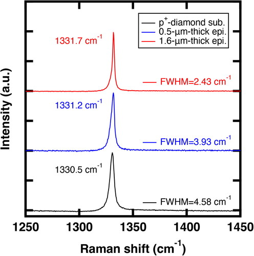
The crystalline quality of the diamond epilayer grown on p+-diamond substrate in macro- and micro-scales was evaluated by XRD and Raman measurements. shows the (a) X-ray rocking curve and (b) 2θ-ω scan profiles of 004 diamond reflection. Due to that the thickness of the diamond epilayer being too thin, the reflection from the substrate was predominant. The peak width (full-width at half maximum: FWHM value) of the rocking curve profiles was ∼70 arcsec. The absolute lattice constant of the substrates was estimated to be 3.567 Å, the same value as the bulk diamond [Citation33]. The increase of boron concentration in the substrate would produce a larger lattice constant [Citation34, Citation35]. shows the Raman spectra of p+-diamond substrate (black line), 0.5-μm thick diamond epilayer (blue line), and 1.6-μm thick diamond epilayer (red line). The p+-diamond substrate exhibits a considerably downshifted peak position from the bulk value (1332 cm−1) [Citation36] and a broadened FWHM value. In contrast, in the case of the diamond epilayer, the peak position approaches the bulk value, and the FWHM values become narrow with increasing the epilayer thickness.
Figure 2. XRD profiles of diamond epilayer/p+-diamond substrate structure. (a) X-ray rocking curve and (b) 2θ-ω scan profiles of 004 diamond reflection.
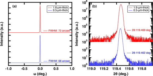
Figure 3. Raman spectra. Black, blue, and red lines correspond to the spectra of p+-diamond substrate, 0.5-μm thick diamond epilayer, and 1.6-μm thick diamond epilayer, respectively.
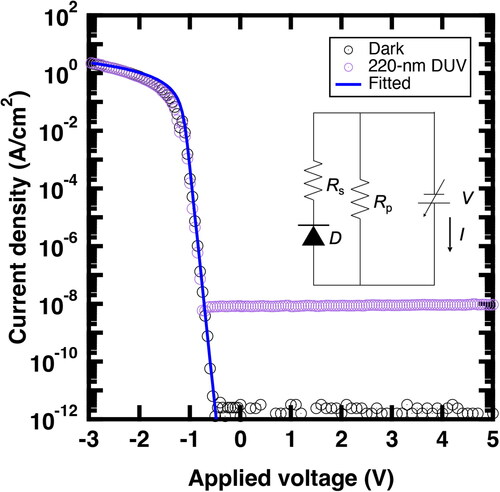
Next, the electric property of the SBPD was investigated. shows the current-voltage (I-V) characteristics of the SBPD. Here the 0.5-μm-thick diamond epilayer grown on p+-diamond substrate was used for the SBPD. The I-V characteristics in the dark and 220-nm DUV light illumination are shown by black and violet circles, respectively. The forward and reverse voltages correspond to negative and positive biases, respectively. The dark I-V characteristics exhibit excellent rectifying properties with a current on/off ratio of 1012 at ±5 V and the apparent threshold voltage of 1.2-1.5 V. The SBPDs were operable in either photovoltaic or reverse-bias mode. The dark I-V curves were fitted by a conventional equivalent circuit model (inset) using a diode, series resistance (Rs), and parallel resistance (Rp). The equation based on the thermionic emission model [Citation37] is given by
(6)
(6)
where I0, A*, VSBH, n, kB, and T are the saturation current, Richardson constant, Schottky barrier height, ideality factor, Boltzmann constant, and temperature, respectively. The A* was assumed to be 90 A/cm2 [Citation38]. The Rs and Rp were resistance components that affect forward and reverse bias characteristics, respectively. Hence, the Rs and Rp were expected to be small and large, respectively. The fitted results are shown by the blue line in . The VSBH, n, and Rs were estimated to be 1.48–1.50 eV, 1.04–1.06, and 0.77 Ω cm2, respectively. Here, the Rp was ignored because of the extremely small leakage current in reverse bias mode. The experimentally obtained Rs of 0.77 Ω cm2 from the I-V curve was much higher than 3.12 mΩ cm2, which was estimated from the film thickness, carrier concentration, and mobility of 0.5 μm, ∼1 × 1014 cm−3, and 1000 cm2/V s, respectively. The high Rs may be due to the inhomogeneous boron concentration and crystal defects in the p+-diamond substrate [Citation39].
Figure 4. I-V characteristics of diamond-based vertical-type SBPD. Black and violet open circles correspond to dark and 220-nm DUV light illumination characteristics, respectively. The inset shows the equivalent circuit used for the fit. The solid line is the fitted curve.
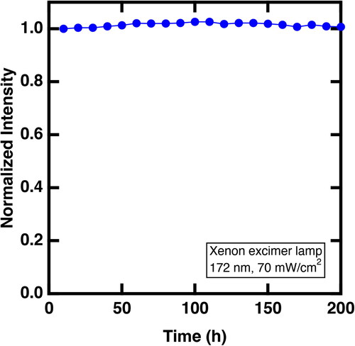
Next, the spectral response characteristics of DUV light and the stability of the SBPDs were evaluated at zero bias in photovoltaic mode [Citation40]. shows the sensitivity as a function of wavelength evaluated by the irradiation of the deuterium D2 lamp. The SBPDs have an obvious response in the DUV region. The peak wavelength was 182 nm with sensitivity at 46 ± 1 mA/W, corresponding to a QE of ∼31%. The QE is 10 times higher than SBPDs for the illumination of 220-nm UV light [Citation23], which is attributed to the large bandgap energy of ∼6.8 eV with a direct transition at Γ point [Citation1]. The devices exhibit a fast response speed of less than 1 sec for the 220-nm UV light without the charge-up effect and persistent photoconductivity owing to the highly conductive diamond substrates (). The angle dependence of the 185-nm DUV light on the photocurrent revealed a reduction of ∼35% at a take-off angle of 45°, where 0° was surface-normal geometry (). shows the stability of the device evaluated by 70 mW/cm2 xenon excimer lamp at zero bias in photovoltaic mode. The intensity was obtained by the output current normalized by the initial photocurrent, considering the reduction of the intensity of the light source. We confirmed that the device showed highly stable operation for 200 hrs without degradation.
Figure 5. Spectral response characteristics. (a) Sensitivity as a function of wavelength, (b) response property, and (c) light angle dependence on the photocurrent.
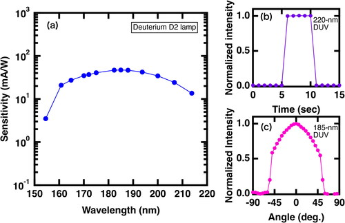
Figure 6. Stability evaluated by 172-nm xenon excimer lamp with 70 mW/cm2.
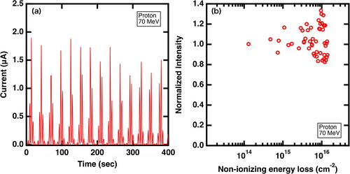
Next, the response property under protons irradiation and the stability of the SBPDs were evaluated at zero bias in photovoltaic mode. shows the response property and stability of the device under the 70 MeV protons irradiation at zero bias in photovoltaic mode. Here the 1.6-μm-thick diamond epilayer was used for the SBPD. The discrete response signal was obtained due to the sample scanning (). Under the huge amount of radiation flux of 10 MGy, the device exhibited stable response properties without charge-up effect and persistent photoconductivity, similar to the photodetectors for excimer lamp. The detected current values of ∼1.5 μA indicated that the collection efficiency was estimated to be ∼13%. Although the estimation of the normalized intensity was not accurate well due to the sample scanning, a significant reduction in the detection efficiency was not observed up to 10-MGy dose of protons corresponding to the non-ionizing energy loss of 1.4 × 10¹⁶ MeV neq/cm2 ().
Figure 7. Response property and stability evaluated by 70 MeV protons. (a) Current generated by protons as a function of time and (b) normalized current intensity as a function of non-ionizing energy loss.
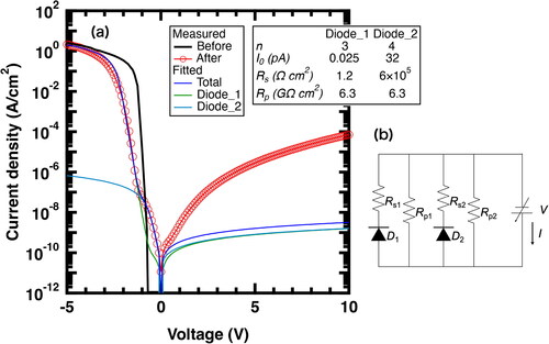
Finally, the dark I-V characteristics of the SBPDs before and after the irradiation of 70 MeV protons was investigated to discuss the appropriate device operation mode for the monitors. shows the dark I-V characteristics of the SBPDs before and after the irradiation by high-energy protons. The forward and reverse voltages correspond to negative and positive biases, respectively. Before the irradiation of protons, the device exhibited excellent rectifying properties with the current on/off ratio of ∼1012, showing the ideality factor of 1.16 and Rs of 1.2 Ω cm2. After the irradiation of protons, the forward current exhibited two-step profiles, and the reverse current increased up to ∼3 × 10⁻⁴ A/cm2 at 10 V. These results indicated that defects were generated by irradiating protons, which increased the On-resistance at forward bias mode and leakage current path at reverse bias mode. Due to the two-step profiles, we used the equivalent circuit model shown in , which consists of two parallel diodes with Rs and Rp components for fitting [Citation41]. The parameters obtained by fitting were inset in . The model explained the forward I-V characteristics with two diode components (diode_1 and diode_2). Therefore, the diode_2 is dominant at biases lower than 1 V, while diode_1 is dominant at biases higher than 1 V. However, this model could not fit the reverse I-V characteristics well. Therefore, another mechanism for the leakage current path was dominant in this case. Several fitting models, such as thermionic-field emission [Citation42, Citation43] and Pool-Frenkel emission [Citation44], were adopted to fit the reverse I-V curve. More than two equations were required to fit the experimental data. Hence, at least two electrical transport mechanisms should be considered. The mechanisms for the leakage current flow were not clear at this moment. Although the protons caused the radiation damage, the response property at zero bias in photovoltaic mode was insensitive to the irradiation damage. Possibly, the reason is due to that no electric field induced the carrier injection occurs at zero bias, which does not modify the photo-carriers generation and recombination. Therefore, the zero bias photovoltaic mode is appropriate for detecting DUV light and protons, which applies to the monitors.
Figure 8. Dark I-V characteristics before and after irradiation of 70 MeV protons. (a) Measured and fitted I-V curves and (b) equivalent circuit used for the fit.
4. Conclusion
We investigated the response property and stability of diamond-based SBPDs by irradiating DUV light with a 172-nm xenon excimer lamp having a power density of 70 mW/cm2 and high-energy protons with an energy of 70 MeV. Using a thin insulating diamond epilayer, electrically conductive diamond substrate, and thermally stable WC-based electrodes were the critical factors in obtaining the vertical-type SBPDs with negligible charge-up effect and persistent photoconductivity. The radiation stability indicates that the zero bias photovoltaic operation mode is appropriate as the monitors for high flux excimer lamps and high-energy protons.
Acknowledgements
The authors wish to acknowledge Dr. H. Takatsuka and Dr. M. Niigaki, Hamamatsu Photonics K.K., for supporting the experiments using DUV light and for helpful discussion. The authors also wish to thank the accelerator staff at CYRIC, Tohoku Univ., for supplying the excellent beams used in this work. This work was partly supported by World Premier International Research Center Initiative (WPI), Ministry of Education, Culture, Sports, Science and Technology (MEXT), Japan.
Disclosure statement
The authors declare no conflict of interest.
Additional information
Funding
Notes on contributors
Masataka Imura
Dr. Masataka Imura is now a principal researcher at the National Institute for Materials Science (NIMS), Japan. He received a Ph.D. in Nitride Semiconductors from Meijo University (Nagoya, Japan), in 2007. He was 21st COE research fellow in 2004-2005 and JSPS research fellow (DC2) in 2006. After that, he got a research position at NIMS. His research interest includes wide-bandgap semiconductor materials (mainly diamond and nitrides) and their photonic and electronic devices.
Manabu Togawa
Dr. Manabu Togawa is now an associate professor at the High Energy Accelerator Research Organization (KEK), Japan. He received a Ph.D. in Nuclear Physics from Kyoto University (Kyoto, Japan) in 2008. He was a special postdoctoral researcher at RIKEN from 2007-2009 and an assistant professor at Osaka University from 2009-2017. In 2017, he got a current position at KEK. His research interest includes particle physics and semiconductor detector for its experiment.
Masaya Miyahara
Dr. Masaya Miyahara is now an associate professor at KEK, Japan. He received a Ph.D. in Physical Electronics from Tokyo Institute of Technology (Tokyo, Japan) in 2009. He was an associate professor at Tokyo Institute of Technology from 2009-2017. In 2017, he got a current position at KEK. His research interest includes mixed-signal circuits and sensor read-out LSI for particle and nuclear physics experiments.
Hironori Okumura
Dr. Hironori Okumura is now an assistant professor at the University of Tsukuba (Tsukuba Japan). He received a Ph.D. in the Growth of Nitride Semiconductors from Kyoto University (Kyoto, Japan) in 2012. He was a JSPS research fellow (DC1) in 2010-2012, a JSPS overseas research fellow at UCSB (US) in 2013-2014, and worked at NTT basic research laboratories (Japan) as a research associate in 2015.After that, he got the current position while working as a visiting researcher at EPFL (Switzerland) in 2016 and MIT (US) in 2017-2018. His research interest includes wide-bandgap semiconductor materials (mainly oxides and nitrides) and their photonic and electronic devices.
Jiro Nishinaga
Dr. Jiro Nishinaga is now a senior research scientist at the National Institute of Advanced Industrial Science and Technology (AIST), Japan. He received a Ph.D. in Compound Semiconductors from Waseda University (Tokyo, Japan) in 2008. He was a research associate at Waseda University in 2007. In 2014, he got a research position at AIST. His research interest includes compound semiconductor materials and solar cells.
Meiyong Liao
Dr. Meiyong Liao is now a chief researcher at NIMS, Japan. He received a Ph.D. in Materials Science for Semiconductors from Chinese Academy of Science (Beijing, China) in 2002. After two years of visiting researcher at Kyoto University, he joined diamond research group at NIMS in 2004. In 2008, he was employed as a permanent researcher at NIMS. He had also been a visiting researcher (2008) at CNRS, France, and Marie Curie Research Fellow (2014-2015) at Aston University, England. His research interest includes wide bandgap semiconductor materials (mainly diamond), photonic and electronic devices, MEMS/NEMS, and device physics.
Yasuo Koide
Dr. Yasuo Koide is now a senior scientist with special mission and a group leader of the next-generation semiconductor group at NIMS, Japan. He received a Ph.D. in Crystal Growth from Nagoya University (Nagoya, Japan) in 1988. He was a vice president at NIMS from 2016-2019. His research interest includes wide bandgap semiconductor materials (mainly diamond and nitrides) and metal/semiconductor contact properties.
References
- Roberts RA, Walker WC. Optical study of the electronic structure of diamond. Phys. Rev. 1967;161(3):730–735.
- Nahum J, Halperin A. Excitation spectra and temperature dependence of luminescence and photoconductivity of diamond. J Phys Chem Solids. 1962;23(4):345–358.
- Binari SC, Marchywka M, Koolbeck DA, et al. Diamond metal-semiconductor-metal ultraviolet photodetectors. Diamond Related Mater. 1993;2(5-7):1020–1023.
- Vaitkus R, Inushima T, Yamazaki S. Enhancement of photosensitivity by ultraviolet irradiation and photoconductivity spectra of diamond thin films. Appl Phys Lett. 1993;62(19):2384–2386.
- Mckeag RD, Chan SSM, Jackman RB. Polycrystalline diamond photoconductive device with high UV‐visible discrimination. Appl Phys Lett. 1995;67(15):2117–2119.
- BenMoussa A, Schuhle U, Haenen K, et al. PIN diamond detector development for LYRA, the solar VUV radiometer on board PROBA II. Phys Stat Sol (a). 2004;201(11):2536–2541.
- Teraji T, Yoshizaki S, Wada H, et al. Highly sensitive UV photodetectors fabricated using high-quality single-crystalline CVD diamond films. Diamond Rel Mater. 2004;13(4-8):858–862.
- Remes Z, Petersen R, Haenen K, et al. Mechanism of photoconductivity in intrinsic epitaxial CVD diamond studied by photocurrent spectroscopy and photocurrent decay measurements. Diamond Relat Mater. 2005;14(3-7):556–560.
- Balducci A, Marinelli M, Milani E, et al. Extreme ultraviolet single-crystal diamond detectors by chemical vapor deposition. Appl Phys Lett. 2005;86(19):193509.
- Lin CN, Lu YJ, Yang X, et al. Diamond-based all-carbon photodetectors for solar-blind imaging. Adv Opt Mater. 2018;6(15):1800068.
- Lin CN, Zhang ZF, Lu YJ, et al. High performance diamond-based solar-blind photodetectors enabled by Schottky barrier modulation. Carbon. 2022;200:510–516.
- Wei MS, Yao KY, Liu YM, et al. A solar-blind UV detector based on graphene-microcrystalline diamond heterojunctions. Small. 2017;13(34):1701328.
- Chen YC, Lu YJ, Lin CN, et al. Self-powered diamond/β-Ga2O3 photodetectors for solar-blind imaging. J Mater Chem C. 2018;6(21):5727–5732.
- Bauer C, Baumann I, Colledani C, et al. Recent results from the RD42 diamond detector collaboration. Nuclear Instruments Methods Phys Res Sec A Accelerators Spectrometers Detectors Assoc Equip. 1996;383(1):64–74.
- Muskinja M, Cindro V, Gorisek A, et al. Investigation of charge multiplication in single crystalline CVD diamond particle detectors. Nuclear Instruments Methods Phys Res Sect A Accel Spectr Detectors Assoc Equip. 2017;841:162–169.
- Bani L, Alexopoulos A, Artuso M, Unno and RD42 Collaboration, et al. A study of the radiation tolerance of CVD diamond to 70 MeV protons, fast neutrons and 200 MeV pions. Sensors. 2020;20(22):6648.
- Alvarez J, Liao MY, Koide Y. Large deep-ultraviolet photocurrent in metal-semiconductor-metal structures fabricated on as-grown boron-doped diamond. Appl Phys Lett. 2005;87(11):113507.
- Liao MY, Sang LW, Teraji T, et al. Comprehensive investigation of single crystal diamond Deep-Ultraviolet detectors. Jpn J Appl Phys. 2012;51(9R):090115.
- Liao MY, Alvarez J, Koide Y. Thermal stability of diamond photodiodes using tungsten carbide as Schottky contact. Jpn J Appl Phys. 2005;44(11):7832–7838.
- Liao MY, Koide Y, Alvarez J. Thermally stable visible-blind diamond photodiode using tungsten carbide Schottky contact. Appl Phys Lett. 2005;87(2):022105.
- Liao MY, Koide Y, Alvarez J. Single Schottky-barrier photodiode with interdigitated-finger geometry: application to diamond. Appl Phys Lett. 2007;90(12):123507.
- Liao MY, Koide Y, Alvarez J, et al. Persistent positive and transient absolute negative photoconductivity observed in diamond photodetectors. Phys Rev B. 2008;78(4):045112.
- Imura M, Koide Y, Liao MY, et al. Vertical-type Schottky-barrier photodiode using p-diamond epilayer grown on heavily boron-doped p+-diamond substrate. Diamond Relat Mater. 2008;17(11):1916–1921.
- Imura M, Liao MY, Alvarez J, et al. Schottky-barrier photodiode using p-diamond epilayer grown on p+-diamond substrates. Diamond Relat Mater. 2009;18(2-3):296–298.
- Bormashov VS, Tarelkin SA, Buga SG, et al. Electrical properties of the high quality boron-doped synthetic single-crystal diamonds grown by the temperature gradient method. Diamond Relat Mater. 2013;35:19–23.
- Teraji T, Fiori A, Kiritani N, et al. Mechanism of reverse current increase of vertical-type diamond Schottky diodes. J Appl Phys. 2017;122(13):135304.
- Fewster PF, Andrew NL. Absolute lattice-parameter measurement. J Appl Crystallogr. 1995;28(4):451–458.
- Liao M. Progress in semiconductor diamond photodetectors and MEMS sensors. Functional Diamond. 2021;1(1):29–46.
- Agostinelli S, Allison J, Amako K, et al. Geant4—a simulation toolkit. Nuclear Instr Methods Phys Res Sec A Accel Spectrom Detect Assoc Equip. 2003;506(3):250–303.
- Allison J, Amako K, Apostolakis J, et al. Geant4 developments and applications. IEEE Trans. Nucl. Sci. 2006;53(1):270–278.
- Allison J, Amako K, Apostolakis J, et al. Recent developments in Geant4. Nuclear Instruments Methods Phys Res Sect A Accel Spectr Detectors Assoc Equip. 2016;835:186–225.
- Schlesinger TE, James RB. Chapter 8: CdTe Nuclear Detectors and Applications. In: Hage-Ali M, Siffert P, editor. Semiconductors for room temperature nuclear detector applications. London, UK: Academic Press; 1995. pp. 43.
- Shikata S, Tanno T, Teraji T, et al. Precise measurements of diamond lattice constant using bond method. Jpn J Appl Phys. 2018;57(11):111301.
- Brazhkin VV, Ekimov EA, Lyapin AG, et al. Lattice parameters and thermal expansion of superconducting boron-doped diamonds. Phys Rev B. 2006;74(14):140502.
- Brunet F, Germi P, Pernet M, et al. The effect of boron doping on the lattice parameter of homoepitaxial diamond films. Diamond Relat Mater. 1998;7(6):869–873.
- Solin SA, Ramdas AK. Raman spectrum of diamond. Phys Rev B. 1970;1(4):1687–1698.
- Padovani FA, Stratton R. Field and thermionic-field emission in Schottky barriers. Solid-State Electron. 1966;9(7):695–707.
- Umezawa H, Tokuda N, Ogura M, et al. Characterization of leakage current on diamond Schottky barrier diodes using thermionic-field emission modeling. Diamond Relat Mater. 2006;15(11-12):1949–1953.
- Srimongkon K, Ohmagari S, Kato Y, et al. Boron inhomogeneity of HPHT-grown single-crystal diamond substrates: confocal micro-Raman mapping investigations. Diamond and Related Materials. 2016;63:21–25.
- Liao MY, Koide Y, Alvarez J. Photovoltaic Schottky ultraviolet detectors fabricated on boron-doped homoepitaxial diamond layer. Appl Phys Lett. 2006;88(3):033504.
- Kamiya T, Narushima S, Mizoguchi H, et al. Electrical properties and structure of p-Type amorphous oxide SemiconductorxZnO·Rh2O3. Adv Funct Mater. 2005;15(6):968–974.
- Teraji T, Koizumi S, Koide Y, et al. Electric field breakdown of lateral Schottky diodes of diamond. Jpn J Appl Phys. 2007;46(9):L196–L198.
- Suda J, Yamaji K, Hayashi Y, et al. Nearly ideal current–voltage characteristics of Schottky barrier diodes formed on hydride-vapor-phase-epitaxy-grown GaN free-standing substrates. Appl Phys Express. 2010;3(10):101003.
- Schroeder H. Poole-Frenkel-effect as dominating current mechanism in thin oxide films—an illusion?! J Appl Phy . 2015;117(21):215103.