
 ?Mathematical formulae have been encoded as MathML and are displayed in this HTML version using MathJax in order to improve their display. Uncheck the box to turn MathJax off. This feature requires Javascript. Click on a formula to zoom.
Abstract
Because of its ultrahigh hardness, synthetic diamond has been widely used in advanced manufacturing and mechanical engineering. As an ultra-wide bandgap semiconductor, on the other hand, diamond recently shows a great potential in electronics industry due to its outstanding physical properties. However, like silicon-based electronics, the electrical properties of diamond should be well modulated before it can be practically used in electronic devices. In this work, we briefly review the recent progresses in producing high-quality, electronic grade synthetic diamonds, as well as several typical strategies, from the conventional element doping to the emerging “elastic strain engineering,” (ESE) for tuning the electrical and functional properties of microfabricated diamonds. We also briefly show some device application demonstrations of diamond and outline some remaining challenges that are impeding diamond’s further practical applications as functional devices and offer some perspective for future functional diamond development.
1. Introduction
Diamond is the hardest natural material. Due to its extreme hardness, diamond has been widely used as a precision cutting tool material in advanced manufacturing machinery equipment to achieve high machining quality [Citation1–5]. In addition to its extensive use in mechanical area, diamond also shows great application potential as an electronic material.
As a member of ultra-wide bandgap semiconducting material, diamond owns many excellent physical and chemical properties (e.g. high thermal conductivity, high breakdown field, and high carrier mobility) [Citation6–10]. These outstanding properties make diamond an appealing material for electronics application, especially under certain extreme conditions (such as high temperature, high radiation, etc.) where conventional silicon-based semiconductors can hardly serve [Citation11–14]. Excellent mechanical properties and great electrical application potential make diamond one of the hottest research topics.
In this review, we will introduce some of the latest research work about diamond. The review will start with a brief introduction of diamond synthesis technology. Then we will introduce several strategies for modulating the electrical properties of diamond, including element doping, surface engineering, phase engineering, strain engineering, and defect engineering. Some devices applications of diamond and remaining problems impeding the application of diamond as electronic material are summarized in the last part.
2. Synthetic diamonds for device applications
As a material with excellent mechanical and functional properties, diamond is greatly needed in a wide range of fields. The high cost of natural diamond pushes forward the research of synthetic diamond. Diamond can be divided into single crystal diamond (SCD) and polycrystalline diamond (PCD). PCD has higher concentration of defects comparing to SCD due to the presence of grain boundary and the electrical properties of devices made by PCD are significantly limited as a result [Citation15]. Therefore, if we want to exploit diamond’s potential as electronic and optical devices (UV/radiation detector, field-effect transistor, diode, etc.), SCD is a better choice than PCD. In the following part of this review, all the diamonds we talk about are SCDs if there is no specific explanation.
Diamond can be synthesized by two main methods: high pressure and high temperature (HPHT) and chemical vapor deposition (CVD) [Citation16–19]. The HPHT method mimics the formation of natural diamond, which transforms graphite into diamond under HPHT [Citation20,Citation21]. HPHT method is of low cost and high yield. However, this method also has some problems. For example, impurities from air or the catalysts can be easily introduced into diamond during the synthesizing process [Citation22–24]. Also, the synthetic diamond size is limited by the HPHT reaction chamber size, making HPHT diamond not an ideal choice for the semiconductor applications.
Another synthesizing method is CVD [Citation25–28], which allows a lower temperature and pressure condition to synthesize diamond [Citation29]. This technique, especially the micro plasma CVD (MPCVD), has been widely used for growing high-quality and large-size diamond. As shown in , the research of MPCVD SCD growth has been conducted from several different aspects, including the preparation with high growth rate, low dislocation density, large size, and flat surface.
Figure 1. Research progresses of synthetic diamonds. (a) Nitrogen addition to increase diamond growth rate [Citation35], diamond plate with (b) low dislocation density, (c) large size, and (d) flat surface [Citation39,Citation45,Citation49]. (a) Reproduced with permission from ref Citation35, Copyright 2002, The National Academy of Sciences.(b) Reproduced with permission from ref Citation39, Copyright 2014 AIP Publishing LLC. (c) Reproduced with permission from ref Citation45, Copyright 2011 Elsevier B.V. All rights reserved. (d) Reproduced with permission from ref Citation49, Copyright 2005 WILEY-VCH Verlag GmbH & Co. KGaA, Weinheim.
![Figure 1. Research progresses of synthetic diamonds. (a) Nitrogen addition to increase diamond growth rate [Citation35], diamond plate with (b) low dislocation density, (c) large size, and (d) flat surface [Citation39,Citation45,Citation49]. (a) Reproduced with permission from ref Citation35, Copyright 2002, The National Academy of Sciences.(b) Reproduced with permission from ref Citation39, Copyright 2014 AIP Publishing LLC. (c) Reproduced with permission from ref Citation45, Copyright 2011 Elsevier B.V. All rights reserved. (d) Reproduced with permission from ref Citation49, Copyright 2005 WILEY-VCH Verlag GmbH & Co. KGaA, Weinheim.](/cms/asset/f94577c4-6794-41f6-b605-daeb3af43c7d/tfdi_a_2151322_f0001_c.jpg)
It is necessary to increase diamond growth rate as there is a strong demand in both industrial production and academic research [Citation28,Citation30]. The diamond growth mechanism has been investigated extensively [Citation31,Citation32]. One efficient strategy is by increasing plasma density during the growth process [Citation33,Citation34], which can be realized by increasing growth pressure or/and growth power. The addition of nitrogen can improve the diamond growth rate as well [Citation30,Citation35]. C. Yan et al. [Citation35] achieved a diamond growth rate of 150 μm/h under a growth pressure of 200 Torr with nitrogen addition. The optical image of the synthesized diamond is shown in . The sample is yellow due to the presence of single substitutional nitrogen. Q. Liang et al. [Citation30] increased growth pressure to 300 Torr and achieved a growth rate of 165 μm/h.
Low dislocation density is important for the electronic applications of diamond [Citation36,Citation37]. A small number of defects would significantly weaken the electrical properties of diamond semiconductor devices. Some serious defects may even lead to the direct failure of the device. The intrinsic defect within diamond seed is the main defect source for the synthesized diamond. Several strategies can be used to minimize the influence from the seed defects. Takeuchi et al. [Citation38] proposed a two-step growth method for growing diamond with low dislocation density, in which case a buffer layer of low dislocation density was synthesized at low growth rate first, followed by the high-speed growth of low-dislocation diamond on the buffer layer. The use of high-quality seed crystal is also important. Mokuno et al. [Citation39] synthesized low-dislocation diamond using high-quality diamond substrate. The dislocation density is <100 cm−2 for the diamond substrate seed and ∼400 cm−2 for the synthetic diamond after growth ().
Large size is another important parameter [Citation40–42]. Many microelectronics chips have a special demand of the size for integration of large numbers of transistors. Moreover, more chips can be fabricated from one single large-size wafer. Therefore, obtaining large (single crystal) diamond wafers with relatively low cost is another key point of the commercial application of diamond semiconductor devices. Mosaic growth is a popular strategy to realize large size diamond [Citation43]. In this method, several small square diamond substrates are pieced together for growing one large diamond [Citation42,Citation44,Citation45]. shows a 20 mm × 40 mm size diamond wafer prepared through this method [Citation45]. However, defects such as stacking faults, twins, and dislocations can easily form in the junction region between the adjacent diamond seeds during the mosaic growth. Heteroepitaxial growth (i.e. growing diamond on silicon or sapphire) can also achieve the large-size diamond growth, but with a high dislocation density [Citation46].
The flat surface of diamond is important as well [Citation47–50], which is not only essential for diamond optics, but also ideal for the heterogeneous integration of diamond with other materials (e.g. GaN). Okushi et al. [Citation48] successfully synthesized diamond with an atomically flat (001) surface, of which the roughness was reduced to 0.04 nm. However, the low growth rate of only tens of nanometers per hour cannot meet the requirement of industrial production. Bogdan et al. [Citation49] improved diamond growth rate to 5 μm/h and guaranteed a low surface roughness of about 0.6 nm at the same time ().
Despite all these progresses, it is hard to achieve all the above requirements (high growth rate, low dislocation density, flat surface, etc.) in one sample, and tradeoffs are often made. For example, nitrogen addition is a common method to increase diamond growth rate [Citation35], but this will introduce nitrogen impurity into diamond, which is not ideal for electronic-grade SCD. Another example is by using low growth temperature and methane content to grow diamond with low dislocation density or high-quality surface [Citation39,Citation48], but these growth parameters will result in low plasma density and reduce diamond growth rate significantly. Some strategies can be used to handle these conflicts. For example, it is feasible to achieve both high speed and high quality growth by using specially designed, high-power MPCVD device [Citation33,Citation34]. High device power has high requirement for MPCVD device. And it is more difficult to modulate plasma status under high power condition. With the development of MPCVD device, the improvement of seed crystal quality and diamond synthesizing technique, one can expect to see mass production of large-size and high-quality SCD in near future.
3. Modulating diamond’s electrical properties
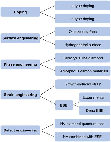
Diamond has a great potential in semiconductor field as it owns excellent physical properties. However, intrinsic diamond shows an electrically insulating state due to its ultra-wide bandgap (∼5.5 eV). Researchers have been trying different methods in the hope to modulate its electrical properties. These methods are listed in . In this section we will introduce the research progress regarding these strategies.
Figure 2. Strategies for modulating diamond’s electrical properties: element doping, surface engineering, phase engineering, strain engineering, and defect engineering.
3.1. Doping
Element doping can be divided into p-type or n-type depending on the electrical conductivity characteristic of the diamond after dopant incorporation. Element doping is the most conventional and popular way to modulate the electrical properties of diamond, which can be realized by two methods: ion-implantation and doping during diamond growth process [Citation51,Citation52]. In ion-implantation, the accelerating field accelerates the dopant ions to give them the kinetic energy. Then the dopant ions will be implanted into the diamond directly. With such method, the dopant can be introduced into the desired area and the doping concentration can be controlled [Citation53,Citation54].
However, it is hard to achieve a uniform doping in diamond through ion-implantation. Diamond has a rigid lattice structure with ultra-strong covalent bond, which makes it difficult to implant dopant ions into diamond. Also, the dopant concentration distribution for single energy level ion-implantation is close to normal distribution [Citation55]. Multiple energy level or dopant dose ion implantations should be applied to get a relatively uniform dopant distribution. In addition, ion implantation will cause damage to diamond crystal structure and induce extra defects [Citation51,Citation56]. These dopant atoms cannot substitute carbon atoms efficiently and annealing heat treatment is often needed to eliminate these unwanted defects.
To avoid these problems occurred during ion-implantation, dopants are usually incorporated during the diamond growth process. There is a very limited room for the HPHT method to achieve this, although HPHT is effective to produce p-type boron-doped diamond. As shown in , the incorporation of dopant is mainly conducted during the CVD diamond growth process [Citation52], which uses methane and hydrogen as the main source gas for diamond growth [Citation57], and dopant gas such as diborane or phosphine to achieve p- or n-type doping. Uniform dopant distribution can be realized by this method and the number of the unwanted crystallographic defects is much less than that in the ion-implantation.
Figure 3. (a) Schematic of dopant incorporation during CVD diamond growth process. (b) Heavily boron-doped diamond, showing dark color [Citation60]. (c) Phosphorous-doped diamond, showing yellow color [Citation66]. (b) Reproduced with permission from ref Citation60, Copyright 2010 American Institute of Physics. (c) Reproduced with permission from ref Citation66, Copyright 2016 Author(s). Published by AIP Publishing.
![Figure 3. (a) Schematic of dopant incorporation during CVD diamond growth process. (b) Heavily boron-doped diamond, showing dark color [Citation60]. (c) Phosphorous-doped diamond, showing yellow color [Citation66]. (b) Reproduced with permission from ref Citation60, Copyright 2010 American Institute of Physics. (c) Reproduced with permission from ref Citation66, Copyright 2016 Author(s). Published by AIP Publishing.](/cms/asset/fd834f56-5cef-465b-bda1-b833992d0be3/tfdi_a_2151322_f0003_c.jpg)
The most widely used and well-studied p-type dopant for diamond is boron (B) [Citation58–60]. Werner et al. [Citation52] realized B doped of diamond by using BCl3 as boron source. However, the Hall mobility of doped diamond was very low. With the development of the B doping of diamond, the Hall mobility of B doped diamond reached 2200 cm2/(V·s) at room temperature, which is sufficient for semiconductor application use [Citation61]. shows a heavily B-doped diamond, of which the dark color was caused by the high concentration of B [Citation60]. By changing the B concentration, the electronic state of diamond can be tuned from semiconducting to metallic and even superconducting [Citation62]. Although some problems remain to be solved, the preparation of p-type diamond is mature and practical enough for semiconductor devices such as field-effect transistors and Schottky diodes.
On the other hand, n-type doping of diamond is extremely difficult. Various elements (e.g. phosphorus, nitrogen, lithium, and sulfur) have been studied but none of them has given a satisfactory result due to the higher activation energy and low doping efficiency. So far, the best candidate is phosphorus (P), which has been proved to form shallow donor level (∼0.6 eV below conduction band minimum) in diamond [Citation63]. Koizumi et al. [Citation64] realized n-type doping of diamond with Hall mobility of 23 cm2/(V·s) at 500 K by introducing P on diamond (111) surface, followed by a series of studies for increasing the Hall mobility of P-doped diamond [Citation65–67]. Based on the successful attempt of the preparation of the P-doped n-type diamond, along with the B-doped p-type diamond, the first diamond pn junction diode was made in 2001 [Citation68]. Kato et al. [Citation66] realized the highest Hall mobility of 1060 cm2/(V·s) at room temperature for the P-doped diamond by reducing electron concentration to about 1010 cm−3. The optical image of P-doped diamond film can be seen in . Although it is feasible to increase the Hall mobility of n-type diamond by using suitable doping strategies, a series of problems remain, including low solid solubility of doping atom, low ionization efficiency induced by deep donor level and low carrier concentration by charge compensation effect of crystal defects. These problems make it hard to obtain n-type diamond of high electrical conductivity at room temperature and restrict the development of diamond semiconducting devices.
As the single-element-doped diamond (especially n-type doped diamond) cannot fully satisfy the requirement for semiconductor applications, the researchers have been trying to dope diamond with multiple elements (co-doping) and also getting some promising results for both p- and n-type diamonds. For p-type doping, Li et al. [Citation69] realized co-doping of boron and hydrogen in SCD under HPHT condition. The lattice structure of B-H co-doped diamond was more compatible and the carrier concentration and electrical conductivity were also improved compared with the B-doped diamond. Issaoui et al. [Citation70] conducted boron and nitrogen co-doping in SCD under CVD condition, and demonstrated that a small amount of nitrogen addition can significantly limit the formation and propagation of defects and improve the diamond quality. For n-type doping, Hu et al. [Citation71] obtained boron and phosphorus co-doped diamond by ion-implantation. The carrier concentration was similar with that of the P-doped diamond, but the Hall mobility and electrical conductivity were greatly improved. Li et al. [Citation72] realized boron and sulfur co-doping in CVD diamond, of which the solubility of S was improved and the electrical conductivity appears higher than the S-doped diamond.
3.2. Surface engineering
Surface modification of diamond can be realized by using suitable treatments such as oxidation, hydrogenation, and fluorination [Citation73–77]. Surface modification can drastically alter the functional properties of diamond, including electrical, tribological, and electrochemical properties [Citation78–81]. The modulation of diamond’s functional properties by surface modification can be considered as surface engineering. In this section, we will focus on the effects of surface engineering on diamond’s electrical properties. Compared with the conventional doping of bulk diamond, surface modification changes the electrical properties of diamond by the modification on the surface level, but can improve the performance of diamond electronic devices significantly.
Recently, the research of surface engineering for diamond’s electrical property modulation focuses mainly on surface oxygen termination and surface hydrogen termination. Surface oxygen termination is a common treatment for diamond surface. Oxygen-terminated surface can be realized by carboxyl or hydroxyl termination [Citation82–84]. As shown in , carboxylated diamond surface can be realized by various methods [Citation74]. Oxygen-terminated diamond surface shows positive electron affinity and is insulating in both vacuum and air conditions. The oxidation treatment of diamond surface can also improve the diamond purity by removing non-diamond carbon and metallic impurities, which is important in semiconductor field.
Figure 4. Surface engineering of diamond. (a) Carboxylated diamond surface can be realized by various methods [Citation74]. (b) Hydrogenation of diamond by rotating plasma reactor [Citation73]. (c) Schematic of graphite/hBN/hydrogen-terminated diamond [Citation92]. (a) Reproduced with permission from ref Citation74, Copyright 2012 WILEY-VCH Verlag GmbH & Co. KGaA, Weinheim. (b) Reproduced with permission from ref Citation73, Copyright 2010 Elsevier B.V. All rights reserved. (c) Reproduced with permission from ref Citation92, Copyright 2021 the author(s), published by Nature Publishing Group.
![Figure 4. Surface engineering of diamond. (a) Carboxylated diamond surface can be realized by various methods [Citation74]. (b) Hydrogenation of diamond by rotating plasma reactor [Citation73]. (c) Schematic of graphite/hBN/hydrogen-terminated diamond [Citation92]. (a) Reproduced with permission from ref Citation74, Copyright 2012 WILEY-VCH Verlag GmbH & Co. KGaA, Weinheim. (b) Reproduced with permission from ref Citation73, Copyright 2010 Elsevier B.V. All rights reserved. (c) Reproduced with permission from ref Citation92, Copyright 2021 the author(s), published by Nature Publishing Group.](/cms/asset/339584e4-6518-43e0-88ae-bbdee560c209/tfdi_a_2151322_f0004_c.jpg)
Surface hydrogen termination is another popular surface modification technique [Citation85] which can be realized by hydrogen plasma () or annealing at 500 °C under hydrogen atmosphere [Citation73,Citation86]. Hydrogen terminated diamond surface shows specific electrical properties, including p-type electronic conductivity and negative electron affinity [Citation87–89]. A surface resistance of 106 Ω*cm can be reached for hydrogen-terminated diamond [Citation78], which is significantly less than that of normal undoped diamond (∼1016 Ω*cm). A commonly accepted reason for the conductivity of hydrogen-terminated diamond surface is the surface transfer doping mechanism [Citation88]. The introduced hydrogen atoms work as acceptor impurity and increase the hole density near the diamond surface region. Also, the upward band bending occurs due to the C-H surface dipole which can facilitate the hole accumulation [Citation88,Citation90]. On the other side, the negatively charged acceptors can lead to hole scattering and reduce the carrier mobility [Citation85,Citation91]. To avoid this situation, high mobility p-channel wide-bandgap transistors can be made by reducing the surface acceptor density on hydrogen-terminated diamond surface [Citation92]. One of the examples using such strategy is shown in , in which hexagonal boron nitride and graphite were selected as the gate insulator and electrode, and a very high room-temperature Hall mobility (680 cm2 V−1 s−1) was obtained [Citation92].
Surface modification also has some limitations. It can only modulate the diamond properties within surface area in contrast with the conventional element doping of bulk diamond. Although p-type electrical conductivity of diamond can be achieved by hydrogen termination, there is no suitable surface modification strategy to realize n-type electrical conductivity of diamond, which limits its application range severely.
3.3. Phase engineering
Carbon material is a very big family, consisting of many allotropes including diamond, graphite, and fullerene which own distinct properties. Property difference is the result of different microstructures. The research of tuning material property by synthesizing material with different phases or conducting phase transformation can be thought as phase engineering. So far, the research of phase engineering for carbon materials has achieved some important progresses.
Generally, carbon materials can be divided into two types: crystalline carbon and amorphous carbon depending on the possession of long-range order in their lattices or not. Diamond is a typical crystalline carbon material while coal is an example of amorphous carbon material. Tang et al. [Citation93] synthesized a new form of carbon material named “paracrystalline diamond.” The optical image of this “paracrystalline diamond” is shown in . The “paracrystalline diamond” consists of sub-nanometer size paracrystallites which possess crystalline medium range order up to a few atomic shells. This material covers the gap between crystalline carbon and amorphous carbon materials.
Figure 5. Phase engineering of diamond. (a) Optical figure of paracrystalline diamond [Citation93], (b) optical figure of ultrahard, diamond-like amorphous carbon [Citation96]. (a) Reproduced with permission from ref Citation93, Copyright 2021 the author(s), published by Nature Publishing Group. (b) Reproduced with permission from ref Citation96, Copyright 2021 the author(s), published by Nature Publishing Group.
![Figure 5. Phase engineering of diamond. (a) Optical figure of paracrystalline diamond [Citation93], (b) optical figure of ultrahard, diamond-like amorphous carbon [Citation96]. (a) Reproduced with permission from ref Citation93, Copyright 2021 the author(s), published by Nature Publishing Group. (b) Reproduced with permission from ref Citation96, Copyright 2021 the author(s), published by Nature Publishing Group.](/cms/asset/19c3327e-6bd1-4b7a-ac1f-3baa13e88aec/tfdi_a_2151322_f0005_c.jpg)
Pure diamond is a crystal consisting of sp3 hybridized carbon atoms. It has ultra-high hardness but is brittle and has a poor electrical conductivity. In contrast with diamond, graphite with sp2 bonding is soft and electrically conductive. Researchers have been looking for new carbon materials which show good electrical conductivity like graphite and high hardness like diamond. Zhang et al. [Citation94] synthesized amorphous carbon material with a high fraction of sp3. The new carbon materials are semiconducting with a bandgap range of 1.5–2.2 eV, which are smaller than that of diamond and comparable to that of the widely used amorphous silicon. These materials also show good mechanical properties such as high highness and strength, such that the newly synthesized carbon material can even scratch the (001) surface of diamond. The same year, S. Zhang et al. [Citation95] obtained some other semiconducting amorphous carbon materials with band gaps of 0.1-0.3 eV and isotropic super hardness and toughness. Shang et al. [Citation96] successfully synthesized millimeter-sized, transparent, and nearly pure sp3 (up to 97.1%) amorphous carbon for the first time, as shown in . This material consists of many randomly oriented clusters with diamond-like short-/medium-range order and possesses the highest hardness, elastic modulus, and thermal conductivity among all the known amorphous material. These materials also exhibit a wide range of tunable optical bandgap from 1.85 to 2.79 eV.
The key point of phase engineering is to modulate material properties by phase synthetization or transformation. Simulation work can help a lot during this process, such as the prediction of potential material structure and property, the design and optimization of experimental parameters (pressure, temperature, the choice of precursor, etc.). Q. Li et al. [Citation97] reported a monoclinic carbon allotrope named “M-carbon” by ab initio simulation. The calculated hardness and bulk modulus of this “M-carbon” were comparable to diamond, and the simulation result was consistent with experimental work [Citation98]. X. Yang et al. [Citation99] predicted a carbon allotrope by Crystal Structure Analysis by Particle Swarm Optimization (CALYPSO) method. This fully sp3-bonded carbon material was named “V-carbon.” Simulation results indicated that the material had a hardness of 90 GPa and bulk modulus 400 GPa, which was verified by experimental work.
3.4. Strain engineering
Although element doping, surface engineering, and phase engineering have achieved some progresses in tuning diamond’s electrical properties, there are still some limitations as discussed above. Strain engineering is emerging as a new strategy having some advantages to overcome or bypass these limitations.
For a defect-free crystal, the maximum elastic strain that it can sustain at 0 K without losing homogeneity is its ideal strain, which is around 10% [Citation100]. However, the actual elastic strain of most bulk material is 2–3 orders of magnitude lower than the theoretical value due to the unavoidable defects existing within the material. When the geometrical size of the material decreases, the probability of the presence of defect inside the material reduces as well. As a result, the elastic strain of the material becomes closer to its ideal strain before the plastic yield appears. Therefore, nanometer materials can generally sustain far more elastic strain than the materials at macro size. This expands the tuning space for elastic strain engineering (ESE).
3.4.1. Growth-induced strain
Many experimental and theoretical works [Citation101–105] have proved that the physical and chemical properties of materials can be improved or fundamentally changed by ESE. Strained Si technology is a typical example and has brought billions of dollars of product value. In this case, tensile strain is applied to a 10–100 nm width Si channel and the carrier mobility of Si is improved dramatically as a result [Citation106]. One common way to obtain strained Si is by heteroepitaxially growing Si on a suitable substrate to induce lattice mismatch. As we can see in , compressive or tensile strain can be introduced to the silicon film as the Si lattice is compressed or stretched to align with the underlying substrate material which has a different lattice constant [Citation107,Citation108].
Figure 6. The introduction of (a) compressive or (b) tensile strain to silicon by using different substrates [Citation107]. (c) TEM image of GaN/diamond interface [Citation113]. (a) and (b) Reproduced with permission from ref 107, Copyright 2004 IEEE. (c) Reproduced with permission from ref Citation113, Copyright 2020 American Chemical Society.
![Figure 6. The introduction of (a) compressive or (b) tensile strain to silicon by using different substrates [Citation107]. (c) TEM image of GaN/diamond interface [Citation113]. (a) and (b) Reproduced with permission from ref 107, Copyright 2004 IEEE. (c) Reproduced with permission from ref Citation113, Copyright 2020 American Chemical Society.](/cms/asset/725e5fd1-3382-4083-97a6-fff6d6c49b9e/tfdi_a_2151322_f0006_b.jpg)
We wish to borrow the successful experiences of growing strained Si film and obtain locally or wholly strained diamond. Several experimental and theoretical work have demonstrated that the electrical properties of diamond can be modulated with elastic strain applied [Citation109–112]. The research of heteroepitaxial growth of diamond has been conducted extensively as this method has the potential to produce large-size and high-quality diamond. A series of materials have been used as the substrates for diamond heteroepitaxial growth, including GaN, Si, sapphire and cubic boron nitride [Citation113–120]. As the lattice constants of these materials are different from that of diamond, local stress/strains are introduced, especially at the interface between diamond and substrates. is the TEM image of GaN/diamond interface, the local strain/stress is introduced due to the different lattice constants of GaN (a = 318 pm, c =518 pm) and diamond (a = 357pm) [Citation113]. At present, scientists are focused on the growth of diamond with reduced or eliminated interfacial stress in order to obtain high-quality and large-size diamond. Such undesired stress may be used for generating a fixed value of strain on diamond. More work needs to be conducted to obtain diamond with expected strain value.
3.4.2. Elastic strain engineering (ESE)
Diamond is generally thought to be hard, brittle and nearly non-deformable [Citation121]. Deforming a diamond usually means irreversible damage to it. Several methods have been tried to investigate the mechanical properties of diamond since 1930s, including indentation and diamond anvil cell compression [Citation122,Citation123], as shown schematically in . However, the deformation of diamond was small and the strain distribution was nonuniform. The research of diamond’s mechanical properties came to a standstill since then.
Figure 7. Experiment progresses on mechanically straining diamond. The development of diamond deformation strategy, from bulk-size diamond deformation ((a) indentation and (b) DAC compression) [Citation122] to micro-size diamond deformation ((c) nanopillar compression, (d) & (e) nanoneedle bending, (f) microbridge and micro-array stretch) [Citation109,Citation110,Citation124,Citation129]. With the development of deformation strategy, larger and more uniform elastic deformation are being realized. (a) Reprinted courtesy of the National Institute of Standards and Technology, U.S. Department of Commerce. Not copyrightable in the United States. (c) Reproduced with permission from ref Citation124, Copyright 2015 American Chemical Society. (d) Reproduced with permission from ref Citation109, Copyright 2018 the author(s), published by American Association for the Advancement of Science (AAAS). (e) Reproduced with permission from ref Citation129, Copyright 2019 the author(s), published by Nature Communications. (f) Reproduced with permission from ref Citation110, Copyright 2021, American Association for the Advancement of Science.
![Figure 7. Experiment progresses on mechanically straining diamond. The development of diamond deformation strategy, from bulk-size diamond deformation ((a) indentation and (b) DAC compression) [Citation122] to micro-size diamond deformation ((c) nanopillar compression, (d) & (e) nanoneedle bending, (f) microbridge and micro-array stretch) [Citation109,Citation110,Citation124,Citation129]. With the development of deformation strategy, larger and more uniform elastic deformation are being realized. (a) Reprinted courtesy of the National Institute of Standards and Technology, U.S. Department of Commerce. Not copyrightable in the United States. (c) Reproduced with permission from ref Citation124, Copyright 2015 American Chemical Society. (d) Reproduced with permission from ref Citation109, Copyright 2018 the author(s), published by American Association for the Advancement of Science (AAAS). (e) Reproduced with permission from ref Citation129, Copyright 2019 the author(s), published by Nature Communications. (f) Reproduced with permission from ref Citation110, Copyright 2021, American Association for the Advancement of Science.](/cms/asset/5bb38398-661f-4fbe-b881-e503a40c2a8b/tfdi_a_2151322_f0007_c.jpg)
Recently, with the development of advanced micro/nano fabrication and mechanical testing techniques, it becomes feasible to conduct mechanical testing for micro/nano diamond samples. A series of tests including nanopillar compression, nanoneedle bending, microbridge, and micro-array stretch [Citation109,Citation110,Citation124–127] have been conducted for small-size diamond samples. Elastic strain or plastic strain of diamond was observed in these works.
In 2016, J. Wheeler et al. conducted uniaxial compression for micro/nano size diamond pillars for the first time [Citation124]. SEM images of diamond nanopillars were observed successfully before and after compression, as shown in . The diamond pillars showed elastic deformation without obvious plastic deformation before the brittle fracture. A maximum shear strength of 75 GPa was measured, which was close to the theoretical yield stress limit of diamond. However, the elastic deformation of diamond was small and mainly concentrated on the top area of the micro pillar.
A. Banerjee et al. [Citation109] conducted side bending test of diamond nanoneedles. The bending deformation of a nanoneedle during loading process is shown in . The researchers discovered ultralarge, fully reversible elastic deformation of nanoscale diamond needles for the first time. Simulation result indicated that a local (tensile) maximum principal strain of 8.88% was obtained on the tension side of the bent needle, which was much higher than the previously reported bulk diamond elastic limit [Citation128]. A. Nie et al. further investigated the elastic limit of diamond nanoneedle [Citation129]. The TEM image of diamond needle before and during compression is shown in . Their research results showed that <100>-oriented nanoneedles with a diameter of 60 nm exhibited highest elastic tensile strain (13.4%) and tensile strength (125 GPa). These values are comparable with the theoretical elasticity and Griffith strength limit of diamond, thus open up the infinite possibility to modulate diamond’s electronic properties through nanomechanical straining.
3.4.3. Deep elastic strain engineering (DESE)
The realization of ultralarge elastic strain in nanoscale diamond has a significant meaning. On one hand, this opens the door for potential deep ESE (DESE) of diamond, that allows unprecedented properties under extreme strained states. On the other hand, it encourages theoretical calculations of diamond DESE as ultralarge deformation and even complicated coupled deformation modes of diamond were often considered to be impossible before.
Experimentally, the ultrahigh elastic strains achieved during the diamond nanoneedle bending tests were not uniform and limited in a relatively localized region. Moreover, bent nanoneedles have a complex strain condition that one side of the nanoneedle is under tensile strain while the other is under compressive strain. To solve these problems for practical device applications, C. Dang et al. [Citation110] fabricated diamond microbridges and microbridge arrays and conducted in-situ uniform tensile tests, as shown in . The sample size and deformation mode in this experiment were comparable to the actual semiconductor application. The diamond microbridge completely recovered to its original length after strain values of up to 7.5% in cyclic tensile tests. With some improvements, maximum tensile strain of up to 9.7% was achieved before fracture happened. This value approaches the ideal elastic limit [Citation130]. Such a realization of large and uniform elastic strain in diamond microbridge and array is unprecedented. They also demonstrated a bandgap reduction of diamond under tensile strain by first principles calculation and confirmed it by electron energy-loss spectroscopy (EELS), which is important for diamond’s emerging DESE application in future semiconductor field.
On the simulation/modeling side, more possibility can be imagined for a diamond strained in a 3D space with unconventional behavior. However, for conventional computational power, it is hard to design the six-dimensional elastic strain tensor ε (ε1 ≡ ε11, ε2 ≡ ε22, ε3 ≡ ε33, ε4 ≡ ε23, ε5 ≡ ε13, ε6 ≡ ε12) through the most optimal combination of diamond’s normal and shear components due to the vast continua of choices available. In order to deal with this challenge, Z. Shi et al. [Citation131] developed a method combining artificial intelligence and multiscale modeling to find out the most optimal pathway for the ESE of diamond. The results demonstrated that by straining diamond in the most optimal way, diamond can be transformed to a state with lower bandgap while its own uniqueness such as high strength and high thermal conductivity are preserved at the same time. Z. Shi et al. [Citation132] improved their simulation strategies by combining machine learning method and a physics-informed, convolutional neural network technique. The achievable bandgap values of diamond through ESE are shown in . Comparing to their previous work [Citation131], intra-band and inter-band correlation are introduced for calculating energy band and the strategy is believed to be more accurate. This strategy is also more versatile such that a broader range of physical characteristics are considered, such as the mass of electrons and holes which are strong sensitive to noise. The simulation results of C. Liu et al. [Citation111] indicated that when diamond is subjected to constrained shear (CS) strain condition, the stress response shows smooth structural flow characterization which is unprecedented in diamond. The anomalous structural deformation of diamond also has profound impacts on its electronic properties [Citation133]. The bandgap of diamond reduced gradually under CS loading condition and a band gap closure appears at surprisingly modest CS stress condition, leading to diamond’s metallization.
Figure 8. Deep ESE simulations of diamond under straining. (a) Achievable bandgap values of diamond through ESE [Citation132]. (b) Simulation prediction of the local strain distribution (left and middle needles, with compressive and tensile strains distribution) and bandgap distribution (right needle) of bent diamond nanoneedles [Citation112]. (c) Conduction charge distribution (left figure) and electronic band structure (right figure) of diamond lattice under a CS strain ε value of 0.566, which is under superconducting condition [Citation135]. (a) Reproduced with permission from ref Citation132, Copyright 2021 the author(s), published by Nature Publishing Group. (b) Reproduced with permission from ref Citation112, Copyright 2020 the author(s). Published by PNAS. (c) Reproduced with permission from ref Citation135, Copyright 2020 American Physical Society.
![Figure 8. Deep ESE simulations of diamond under straining. (a) Achievable bandgap values of diamond through ESE [Citation132]. (b) Simulation prediction of the local strain distribution (left and middle needles, with compressive and tensile strains distribution) and bandgap distribution (right needle) of bent diamond nanoneedles [Citation112]. (c) Conduction charge distribution (left figure) and electronic band structure (right figure) of diamond lattice under a CS strain ε value of 0.566, which is under superconducting condition [Citation135]. (a) Reproduced with permission from ref Citation132, Copyright 2021 the author(s), published by Nature Publishing Group. (b) Reproduced with permission from ref Citation112, Copyright 2020 the author(s). Published by PNAS. (c) Reproduced with permission from ref Citation135, Copyright 2020 American Physical Society.](/cms/asset/80e2796a-0990-46f7-9925-02e7e33046ba/tfdi_a_2151322_f0008_c.jpg)
The simulation results indicated that when the applied strain reaches a certain level, fundamental changes will happen for diamond’s properties, such as metallization and superconductivity. Z. Shi et al. [Citation112] demonstrated that it is possible to achieve metallization in diamond exclusively through the imposition of reversible elastic strains, without triggering phonon instability or phase transition from diamond to graphite. As can be seen in , for <110>-oriented diamond nanoneedles bending along direction, “safe” metallization can be realized on the local area of compression side with a compressive strain value of ∼10.8% which is less than the theoretically approachable maximum compressive strain of 14.5%. Also, the elastic strain energy density values for “safe” metallization are comparable to what has been demonstrated in experiments of reversible deformation of diamond nanoneedles [Citation109,Citation129]. Diamond can turn into a superconductor with a critical temperature Tc ≈ 4 K near 3% boron doping [Citation134]. C. Liu et al. found that CS loading conditions may affect the superconductivity of diamond as well [Citation135]. The simulation showed that diamond maintained a stable structure under the maximum CS strain of 0.566. The conduction charge distribution and electronic band structure of diamond lattice under this strain value are shown in . The simulation results indicated that superconductivity occurred when the CS strain applied on diamond reached 0.349. A CS-strain driven critical temperature (Tc) of 2.4–12.4K can be reached for Coulomb pseudopotential μ* = 0.15–0.05. These surprisingly high Tc values under realistic μ* place deformed diamond among the most prominent elemental superconductors [Citation136].
3.5. Defect engineering
Diamond often exists with defects such as vacancy, impurity, and structural dislocation. Although these defects make diamond not perfect crystal, they can be useful sometimes for some specific applications, if well controlled. The tuning of material property by adjusting/introducing specific defect in it can be considered as defect engineering. One of the most common impurities existing in diamond is N. In this section, we want to introduce a special N-related defect, nitrogen vacancy (NV) center.
NV center is composed of a substitutional N atom and an adjacent vacancy, as schematically shown in [Citation137]. The spin state of NV center can be initialized or read-out by using suitable laser. The electron spin can be manipulated by external factors (e.g. microwave, magnetic and electric field) at room temperature. These unique properties give diamond great application potentials in quantum information and sensing. As NV center is an ideal solid qubit under room temperature, if NV center can be generated and manipulated, it is possible to build room-temperature quantum computers [Citation138,Citation139]. NV can also serve as an atomic-scale sensor with high sensitivity [Citation140–142]. As we can see in , in biological field, the nanoscale magnetic imaging of ferritins can be realized in a single cell by using the NV center as the sensor [Citation140]. In future, the doctors may use NV center to diagnose the lesion of our body at early stage.
Figure 9. Defect engineering. (a) Schematic of NV center diamond [Citation137]. (b) Magnetic imaging of ferritins in a single cell by NV center [Citation140]. (c) Schematic of manipulating single NV spin by laser [Citation14]. (a) Reproduced with permission from ref Citation137, Copyright 2021 by the authors. Licensee MDPI, Basel, Switzerland. (b) Reproduced with permission from ref Citation140, Copyright 2019 the author(s), published by American Association for the Advancement of Science (AAAS). (c) Reproduced with permission from ref Citation14, Copyright 2014 the author(s), published by Nature Communications.
![Figure 9. Defect engineering. (a) Schematic of NV center diamond [Citation137]. (b) Magnetic imaging of ferritins in a single cell by NV center [Citation140]. (c) Schematic of manipulating single NV spin by laser [Citation14]. (a) Reproduced with permission from ref Citation137, Copyright 2021 by the authors. Licensee MDPI, Basel, Switzerland. (b) Reproduced with permission from ref Citation140, Copyright 2019 the author(s), published by American Association for the Advancement of Science (AAAS). (c) Reproduced with permission from ref Citation14, Copyright 2014 the author(s), published by Nature Communications.](/cms/asset/c4993c9e-4e6d-42f0-8c1c-040377396ad5/tfdi_a_2151322_f0009_c.jpg)
As a nanoscale sensor, NV center is sensitive to the surrounding environment (magnetic, electrical, and strain field, etc.) [Citation14,Citation143,Citation144]. It is possible to modulate the properties of NV center by mechanical strain and researchers have obtained some interesting results. S. Bennett et al. [Citation145] proposed a strategy to realize phonon-induced spin-spin interactions by coupling them via strain introduced by vibrational mode of a diamond mechanical nanoresonator. The spin dephasing and relaxation are depressed significantly by generating substantial squeezed states of a spin ensemble. P. Ovartchaiyapong et al. [Citation14] fabricated diamond cantilever with an embedded nitrogen-vacancy center. As shown in , the couple of mechanical strain and the spin of the NV center is realized by the mechanical motion of the diamond cantilever. The NV center behaved as an atomic-scale sensor and the spin-based strain imaging reached a strain sensitivity of 3*10−6 strain Hz−1/2. A. Barfuss et al. [Citation146] presented a new approach to coherently manipulate a single electronic spin via internal strain. Time-varying stain was applied on a diamond cantilever to generate long-lasting, coherent oscillations of a NV center spin. The phonon-dressed states were observed by direct spectroscopy and the spin coherence time of the NV center was enhanced significantly by the continuous strain.
Overall, several strategies, from the conventional element doping to the ESE for modulating the electrical properties of diamond are reviewed in this section. These different methods are summarized in to help readers have an overview. It is worth mentioning that none of these methods can fully use the outstanding physical properties of diamond and more work is needed to explore and accelerate its application in semiconductor devices.
Table 1. Summarization of all the modulation strategies discussed in this work.
3.6. Electronic device applications of diamond
Nowadays, diamond shows increased application potentials in high frequency/high power semiconductor due to its outstanding properties (wide bandgap, high thermal conductivity, high breakdown field strength, etc.). M. W. Geis et al. [Citation147] successfully fabricated Schottky diode based on B-doped diamond. The maximum work temperature of this device was 700 °C, far beyond that of SiC device (550 ∼ 600 °C). T. Zimmermann et al. [Citation11] introduced a nitrogen doped ultra-nano-crystalline diamond layer into diamond diode. The device showed an extraordinary thermal stability, which worked well up to 1050 °C in vacuum. Besides high working temperature, diamond device can also sustain high electrical field strength. N. Tatsumi et al. [Citation148] manufactured Pt/diamond Schottky diode with a breakdown voltage of 3.1 MV/cm, which was higher than its SiC counterpart.
Diamond also shows great potential in radiation detection field. The inherent properties (ultrawide bandgap, tight crystal lattice, and high covalent bonding energy) of diamond lead to its low radiation damage, rapid charge collection time. A. Balducci et al. [12] successfully increased the charge collection distance from 50 to 300 μm for micro-strip detector and pixel array detector made by diamond. S. Lagomarsino et al. [Citation149] applied 3D concept to diamond detector. The charge collection efficiency reached 95% for their single crystal 3D diamond detector under a low voltage of 3 V and the device just worked fine after radiation.
4. Summary and outlook
As the hardest material in nature, diamond has been widely used in advanced manufacturing and tooling industry. Recent progresses in fabricating high-quality single crystalline diamond also bring unprecedented opportunities to open up functional device applications of diamond as a wide bandgap semiconductor, due to its outstanding electrical properties and figures of merit. The increasing demand of electronic grade diamond pushes forward the research and development (R&D) of synthetic diamonds, especially the latest CVD technique for growing wafer-scale, electronic-grade SCD.
Intrinsic diamond without doping shows electric insulation behavior due to its ultra-wide bandgap. The electrical properties of diamond need to be thus modulated before it being applied into electronic devices. A series of strategies including element doping, surface modification, phase engineering and strain engineering have been developed by researchers, and are reviewed in this paper. The device application of diamond is introduced as well. In addition, the specific properties of NV center in diamond bring a bright future for diamond’s application in quantum information and quantum sensing applications.
Lastly, although diamond has a lot of potentials as a promising electronic material, there are many challenges to be addressed. For the growth of large-size (up to wafer scale) and high-quality diamond, the challenges include improving crystal quality (single crystallinity), reducing the surface roughness and internal flaws, increasing the growth rate without compromising the size and quality, and developing uniform epitaxial growth techniques for strain engineering and device integration. For the development of diamond planar processing technology for strain-engineered devices, some difficulties include the control of crystal orientation, precise geometric shape, and surface morphology and topography. While for the realization of efficient n-type doping of diamond with high electrical conductivity is another challenge for diamond’s microelectronics application. As these problems are gradually going to be addressed with the rapid development in this field, we will witness the rising of functional diamond applications in the near future.
| Abbreviations | ||
| B | = | boron |
| CALYPSO | = | Crystal Structure Analysis by Particle Swarm Optimization |
| CS | = | constrained shear |
| CVD | = | chemical vapor deposition |
| DAC | = | diamond anvil cell |
| DESE | = | deep elastic strain engineering |
| EELS | = | electron energy-loss spectroscopy |
| ESE | = | elastic strain engineering |
| hBN | = | hexagonal boron nitride |
| HPHT | = | high pressure and high temperature MPCVD micro plasma chemical vapor deposition |
| NV | = | nitrogen vacancy |
| P | = | phosphorus |
| PCD | = | polycrystalline diamond |
| R&D | = | research and development |
| SCD | = | single crystalline diamond |
| SEM | = | scanning electron microscope |
| TEM | = | transmission electron microscope |
| UV | = | ultraviolet. |
Acknowledgments
We acknowledge the support from the Research Grants Council of the Hong Kong Special Administrative Region, China, under RFS2021-1S05 and the National Natural Science Foundation of China under project 11922215. H.Z. acknowledges the funding from the National Natural Science Foundation of China (Grant 11902200) and the Science and Technology Commission of Shanghai Municipality (Grant 19YF1433600). Also, we thank Drs. Maoyuan Li and Yuan Hou for fruitful discussions.
Disclosure statement
No potential conflict of interest was reported by the authors.
Funding
This work was supported by Research Grants Council of the Hong Kong Special Administrative Region, China, under RFS2021-1S05 and the National Natural Science Foundation of China under project 11922215 and Grant 11902200 and the Science and Technology Commission of Shanghai Municipality (Grant 19YF1433600), University Grants Committee, and Shanghai Science and Technology Committee.
References
- Harano K, Satoh T, Sumiya H. Cutting performance of nano-polycrystalline diamond. Diamond Relat Mater. 2012;24:78–82.
- Wentorf R, DeVries RC, Bundy F. Sintered superhard materials. Science. 1980;208(4446):873–880.
- Goncharenko IN. Neutron diffraction experiments in diamond and sapphire anvil cells. High Pressure Res. 2004;24(1):193–204.
- Moseley SG, Bohn KP, Goedickemeier M. Core drilling in reinforced concrete using polycrystalline diamond (PCD) cutters: wear and fracture mechanisms. Int J Refract Met Hard Mater. 2009;27(2):394–402.
- Sun FH, Zhang ZM, Chen M, et al. Improvement of adhesive strength and surface roughness of diamond films on Co-cemented tungsten carbide tools. Diamond Relat Mater. 2003;12(3–7):711–718.
- Matsumoto S, Sato Y, Kamo M, et al. Vapor deposition of diamond particles from methane. Jpn J Appl Phys. 1982;21(4):L183–L185.
- Ueda K, Kasu M, Yamauchi Y, et al. Diamond FET using high-quality polycrystalline diamond with f T of 45 GHz and f max of 120 GHz. IEEE Electron Device Lett. 2006;27(7):570–572.
- Taniuchi H, Umezawa H, Arima T, et al. High-frequency performance of diamond field-effect transistor. IEEE Electron Device Lett. 2001;22(8):390–392.
- Kurihara K, Sasaki K, Kawarada M, et al. High rate synthesis of diamond by dc plasma jet chemical vapor deposition. Appl Phys Lett. 1988;52(6):437–438.
- Isberg J, Hammersberg J, Johansson E, et al. High carrier mobility in single-crystal plasma-deposited diamond. Science. 2002;297(5587):1670–1672.
- Zimmermann T, Kubovic M, Denisenko A, et al. Ultra-nano-crystalline/single crystal diamond heterostructure diode. Diamond Relat Mater. 2005;14(3–7):416–420.
- Balducci A, De Sio A, Marinelli M, et al. Extreme UV single crystal diamond photodetectors by chemical vapor deposition. Diamond Relat Mater. 2005;14(11–12):1980–1983.
- Dhomkar S, Henshaw J, Jayakumar H, et al. Long-term data storage in diamond. Sci Adv. 2016;2(10):e1600911.
- Ovartchaiyapong P, Lee KW, Myers BA, et al. Dynamic strain-mediated coupling of a single diamond spin to a mechanical resonator. Nat Commun. 2014;5:4429.
- Sharda T, Sikder AK, Misra DS, et al. Studies of defects and impurities in diamond thin films. Diamond Relat Mater. 1998;7(2–5):250–254.
- Palyanov YN, Borzdov YM, Khokhryakov AF, et al. Effect of nitrogen impurity on diamond crystal growth processes. Crystal Growth Design. 2010;10(7):3169–3175.
- Eaton-Magana S, Shigley JE. Observations on CVD-Grown synthetic diamonds: a review. Gems Gemol. 2016;52:222–245.
- Asmussen J, Grotjohn TA, Schuelke T, et al. Multiple substrate microwave plasma-assisted chemical vapor deposition single crystal diamond synthesis. Appl Phys Lett. 2008;93(3):031502.
- Schreck M, Asmussen J, Shikata S, et al. Large-area high-quality single crystal diamond. MRS Bull. 2014;39(6):504–510.
- Bundy FP, Hall HT, Strong HM, et al. Man-made diamonds. Nature. 1955;176(4471):51–55.
- Wentorf RH. Diamond growth rates. J Phys Chem. 1971;75(12):1833–1837.
- Liang ZZ, Jia X, Ma HA, et al. Synthesis of HPHT diamond containing high concentrations of nitrogen impurities using NaN3 as dopant in metal-carbon system. Diamond Relat Mater. 2005;14(11–12):1932–1935.
- Kanda H. Colored high pressure high temperature (HPHT) synthetic diamonds. Radiat Eff Defects Solids. 2001;156(1-4):163–172.
- Palyanov YN, Kupriyanov IN, Khokhryakov AF, et al. High-pressure crystallization and properties of diamond from magnesium-based catalysts. CrystEngComm. 2017;19(31):4459–4475.
- Eversole WG, April 17. Synthesis of diamond. US Patent, 3,030188. 1962.
- Wang T, Xin HW, Zhang ZM, et al. The fabrication of nanocrystalline diamond films using hot filament CVD. Diamond Relat Mater. 2004;13(1):6–13.
- Smith JA, Rosser KN, Yagi H, et al. Diamond deposition in a DC-arc jet CVD system: investigations of the effects of nitrogen addition. Diamond Relat Mater. 2001;10(3–7):370–375.
- Chayahara A, Mokuno Y, Horino Y, et al. The effect of nitrogen addition during high-rate homoepitaxial growth of diamond by microwave plasma CVD. Diamond Relat Mater. 2004;13(11–12):1954–1958.
- Werner M, Locher R. Growth and application of undoped and doped diamond films. Rep Prog Phys. 1998;61(12):1665–1710.
- Liang Q, Chin CY, Lai J, et al. Enhanced growth of high quality single crystal diamond by microwave plasma assisted chemical vapor deposition at high gas pressures. Appl Phys Lett. 2009;94(2):024103.
- Silva F, Achard J, Brinza O, et al. High quality, large surface area, homoepitaxial MPACVD diamond growth. Diamond Relat Mater. 2009;18(5–8):683–697.
- Goodwin DG. Scaling laws for diamond chemical‐vapor deposition. I. Diamond surface chemistry. J Appl Phys. 1993;74(11):6888–6894.
- Silva F, Hassouni K, Bonnin X, et al. Microwave engineering of plasma-assisted CVD reactors for diamond deposition. J Phys: condens Matter. 2009;21(36):364202.
- Gicquel A, Derkaoui N, Rond C, et al. Quantitative analysis of diamond deposition reactor efficiency. Chem Phys. 2012;398:239–247.
- Yan CS, Vohra YK, Mao HK, et al. Very high growth rate chemical vapor deposition of single-crystal diamond. Proc Natl Acad Sci USA. 2002;99(20):12523–12525.
- Lubeigt W, Bonner GM, Hastie JE, et al. Continuous-wave diamond raman laser. Opt Lett. 2010;35(17):2994–2996.
- Umezawa H, Ikeda K, Tatsumi N, et al. Device scaling of pseudo-vertical diamond power schottky barrier diodes. Diamond Relat Mater. 2009;18(9):1196–1199.
- Takeuchi D, Yamanaka S, Watanabe H, et al. High quality homoepitaxial diamond thin film synthesis with high growth rate by a two-step growth method. Diamond Relat Mater. 1999;8(6):1046–1049.
- Mokuno Y, Kato Y, Tsubouchi N, et al. A nitrogen doped low-dislocation density free-standing single crystal diamond plate fabricated by a lift-off process. Appl Phys Lett. 2014;104(25):252109.
- Tallaire A, Barjon J, Brinza O, et al. Dislocations and impurities introduced from etch-pits at the epitaxial growth resumption of diamond. Diamond Relat Mater. 2011;20(7):875–881.
- Mokuno Y, Chayahara A, Yamada H, et al. Improving purity and size of single-crystal diamond plates produced by high-rate CVD growth and lift-off process using ion implantation. Diamond Relat Mater. 2009;18(10):1258–1261.
- Yamada H, Chayahara A, Mokuno Y, et al. A 2-in. mosaic wafer made of a single-crystal diamond. Appl Phys Lett. 2014;104(10):102110.
- Janssen G, Giling L. “Mosaic” growth of diamond. Diamond Relat Mater. 1995;4(7):1025–1031.
- Kobashi K, Nishibayashi Y, Yokota Y, et al. R&D of diamond films in the frontier carbon technology project and related topics. Diamond Relat Mater. 2003;12(3–7):233–240.
- Yamada H, Chayahara A, Umezawa H, et al. Fabrication and fundamental characterizations of tiled clones of single-crystal diamond with 1-inch size. Diamond Relat Mater. 2012;24:29–33.
- Schreck M, Gsell S, Brescia R, et al. Ion bombardment induced buried lateral growth: the key mechanism for the synthesis of single crystal diamond wafers. Sci Rep. 2017;7(1):44462.
- Aleksov A, Kubovic M, Kasu M, et al. Diamond-based electronics for RF applications. Diamond Relat Mater. 2004;13(2):233–240.
- Okushi H, Watanabe H, Ri S, et al. Device-grade homoepitaxial diamond film growth. J Cryst Growth. 2002;237–239:1269–1276.
- Bogdan G, Nesládek M, D’Haen J, et al. Growth and characterization of near‐atomically flat, thick homoepitaxial CVD diamond films. Phys Stat Solidi (a). 2005;202(11):2066–2072.
- Teraji T, Hamada M, Wada H, et al. High-quality homoepitaxial diamond (100) films grown under high-rate growth condition. Diamond Relat Mater. 2005;14(11–12):1747–1752.
- Tsubouchi N, Ogura M, Horino Y, et al. Low-resistance p + layer formation into diamond using heavily B ion implantation. Appl Phys Lett. 2006;89(1):012101.
- Werner M, Dorsch O, Baerwind HU, et al. Charge transport in heavily B‐doped polycrystalline diamond films. Appl Phys Lett. 1994;64(5):595–597.
- Scott EA, Hattar K, Braun JL, et al. Orders of magnitude reduction in the thermal conductivity of polycrystalline diamond through carbon, nitrogen, and oxygen ion implantation. Carbon. 2020;157:97–105.
- Smith JM, Meynell SA, Bleszynski Jayich AC, et al. Colour Centre generation in diamond for quantum technologies. Nanophotonics. 2019;8(11):1889–1906.
- Haque A, Sumaiya S. An overview on the formation and processing of Nitrogen-Vacancy photonic centers in diamond by ion implantation. JMMP. 2017;1(1):6.
- Agulló-Rueda F, Gordillo N, Ynsa MD, et al. Lattice damage in 9-MeV-carbon irradiated diamond and its recovery after annealing. Carbon. 2017;123:334–343.
- Kobashi K, Nishimura K, Kawate Y, et al. Synthesis of diamonds by use of microwave plasma chemical-vapor deposition: morphology and growth of diamond films. Phys Rev B. 1988;38(6):4067–4084.
- Sato H, Tomokage H, Kiyota H, et al. Transient current measurements after applying the electron-beam pulse on boron-doped homoepitaxial diamond films. Diamond Relat Mater. 1998;7(8):1167–1171.
- Yamanaka S, Takeuchi D, Watanabe H, et al. Low‐compensated boron‐doped homoepitaxial diamond films using trimethylboron. Phys Stat Solidi (a). 1999;174(1):59–64.
- Issaoui R, Achard J, Silva F, et al. Growth of thick heavily boron-doped diamond single crystals: effect of microwave power density. Appl Phys Lett. 2010;97(18):182101.
- Yap CM, Ansari K, Xiao S, et al. Properties of near-colourless lightly boron doped CVD diamond. Diamond Relat Mater. 2018;88:118–122.
- Ashfold MNR, Goss JP, Green BL, et al. Nitrogen in diamond. Chem Rev. 2020;120(12):5745–5794.
- Grotjohn TA, Tran DT, Yaran MK, et al. Heavy phosphorus doping by epitaxial growth on the (111) diamond surface. Diamond Relat Mater. 2014;44:129–133.
- Koizumi S, Kamo M, Sato Y, et al. Growth and characterization of phosphorous doped {111} homoepitaxial diamond thin films. Appl Phys Lett. 1997;71(8):1065–1067.
- Kato H, Yamasaki S, Okushi H. n-type doping of (001)-oriented single-crystalline diamond by phosphorus. Appl Phys Lett. 2005;86(22):222111.
- Kato H, Ogura M, Makino T, et al. N-type control of single-crystal diamond films by ultra-lightly phosphorus doping. Appl Phys Lett. 2016;109(14):142102.
- Kato H, Makino T, Yamasaki S, et al. n-type diamond growth by phosphorus doping on (0 0 1)-oriented surface. J Phys D Appl Phys. 2007;40(20):6189–6200.
- Koizumi S, Watanabe K, Hasegawa M, et al. Ultraviolet emission from a diamond pn junction. Science. 2001;292(5523):1899–1901.
- Li Y, Jia X, Ma HA, et al. Electrical properties of diamond single crystals co-doped with hydrogen and boron. CrystEngComm. 2014;16(32):7547.
- Issaoui R, Tallaire A, Mrad A, et al. Defect and threading dislocations in single crystal diamond: a focus on boron and nitrogen codoping. Phys Status Solidi A. 2019;216(21):1900581.
- Hu XJ, Li RB, Shen HS, et al. Electrical and structural properties of boron and phosphorus co-doped diamond films. Carbon. 2004;42(8–9):1501–1506.
- Li R, Hu X, Shen H, et al. Co-doping of sulfur and boron in CVD-diamond. Mater Lett. 2004;58(12–13):1835–1838.
- Girard HA, Arnault JC, Perruchas S, et al. Hydrogenation of nanodiamonds using MPCVD: a new route toward organic functionalization. Diamond Relat Mater. 2010;19(7–9):1117–1123.
- Krueger A, Lang D. Functionality is key: recent progress in the surface modification of nanodiamond. Adv Funct Mater. 2012;22(5):890–906.
- Ray MA, Tyler T, Hook B, et al. Cool plasma functionalization of nano-crystalline diamond films. Diamond Relat Mater. 2007;16(12):2087–2089.
- Sotowa KI, Amamoto T, Sobana A, et al. Effect of treatment temperature on the amination of chlorinated diamond. Diamond Relat Mater. 2004;13(1):145–150.
- Chen J, Deng SZ, Chen J, et al. Graphitization of nanodiamond powder annealed in argon ambient. Appl Phys Lett. 1999;74(24):3651–3653.
- Landstrass MI, Ravi KV. Resistivity of chemical vapor deposited diamond films. Appl Phys Lett. 1989;55(10):975–977.
- Ferro S, Battisti AD. The 5-V window of polarizability of fluorinated diamond electrodes in aqueous solutions. Anal Chem. 2003;75(24):7040–7042.
- Sine G, Ouattara L, Panizza M, et al. Electrochemical behavior of fluorinated boron-doped diamond. Electrochem Solid-State Lett. 2003;6:9–11.
- Mertens M, Mohr M, Brühne K, et al. Patterned hydrophobic and hydrophilic surfaces of ultra-smooth nanocrystalline diamond layers. Appl Surf Sci. 2016;390:526–530.
- Osswald S, Yushin G, Mochalin V, et al. Control of sp2/sp3 carbon ratio and surface chemistry of nanodiamond powders by selective oxidation in air. J Am Chem Soc. 2006;128(35):11635–11642.
- Krueger A. The structure and reactivity of nanoscale diamond. J Mater Chem. 2008;18(13):1485–1492.
- Martín R, Heydorn PC, Alvaro M, et al. General strategy for High-Density covalent functionalization of diamond nanoparticles using fenton chemistry. Chem Mater. 2009;21(19):4505–4514.
- Li Y, Zhang JF, Liu GP, et al. Mobility of two-dimensional hole gas in H-terminated diamond. Phys Status Solidi RRL. 2018;12(3):1700401.
- Ahmed ASHEKI, Mandal S, Gines L, et al. Low temperature catalytic reactivity of nanodiamond in molecular hydrogen. Carbon. 2016;110:438–442.
- Cui J, Ristein J, Ley L. Electron affinity of the bare and hydrogen covered single crystal diamond (111) surface. Phys Rev Lett. 1998;81(2):429–432.
- Maier F, Riedel M, Mantel B, et al. Origin of surface conductivity in diamond. Phys Rev Lett. 2000;85(16):3472–3475.
- Bandis C, Pate BB. Electron emission due to exciton breakup from negative electron affinity diamond. Phys Rev Lett. 1995;74(5):777–780.
- Petrini D, Larsson K. A theoretical study of the energetic stability and geometry of hydrogen-and oxygen-terminated diamond (100) surfaces. J Phys Chem C. 2007;111(2):795–801.
- Sasama Y, Kageura T, Komatsu K, et al. Charge-carrier mobility in hydrogen-terminated diamond field-effect transistors. J Appl Phys. 2020;127(18):185707.
- Sasama Y, Kageura T, Imura M, et al. High-mobility p-channel wide-bandgap transistors based on hydrogen-terminated diamond/hexagonal boron nitride heterostructures. Nat Electron. 2022;5(1):37–44.
- Tang H, Yuan X, Cheng Y, et al. Synthesis of paracrystalline diamond. Nature. 2021;599(7886):605–610.
- Zhang S, Li Z, Luo K, et al. Discovery of carbon-based strongest and hardest amorphous material. Natl Sci Rev. 2022;9(1):nwab140.
- Zhang S, Wu Y, Luo K, et al. Narrow-gap, semiconducting, superhard amorphous carbon with high toughness, derived from C60 fullerene. Cell Rep Phys Sci. 2021;2(9):100575.
- Shang Y, Liu Z, Dong J, et al. Ultrahard bulk amorphous carbon from collapsed fullerene. Nature. 2021;599(7886):599–604.
- Li Q, Ma Y, Oganov AR, et al. Superhard monoclinic polymorph of carbon. Phys Rev Lett. 2009;102(17):175506.
- Mao WL, Mao H-K, Eng PJ, et al. Bonding changes in compressed superhard graphite. Science. 2003;302(5644):425–427.
- Yang X, Yao M, Wu X, et al. Novel superhard sp^{3} carbon allotrope from Cold-Compressed C_{70} peapods. Phys Rev Lett. 2017;118(24):245701.
- Liu F, Ming P, Li J. Ab initiocalculation of ideal strength and phonon instability of graphene under tension. Phys Rev B. 2007;76(6):064120.
- Sun Y, Thompson SE, Nishida T. Physics of strain effects in semiconductors and metal-oxide-semiconductor field-effect transistors. J Appl Phys. 2007;101(10):104503.
- Süess MJ, Geiger R, Minamisawa RA, et al. Analysis of enhanced light emission from highly strained germanium microbridges. Nat Photon. 2013;7(6):466–472.
- Feng J, Qian X, Huang CW, et al. Strain-engineered artificial atom as a broad-spectrum solar energy funnel. Nature Photon. 2012;6(12):866–872.
- Sundaram RS, Engel M, Lombardo A, et al. Electroluminescence in single layer MoS2. Nano Lett. 2013;13(4):1416–1421.
- Thulin L, Guerra J. Calculations of strain-modified anataseTiO2band structures. Phys Rev B. 2008;77(19):195112.
- Manasevit HM, Gergis IS, Jones AB. Electron mobility enhancement in epitaxial multilayer Si‐Si1 − xGexalloy films on (100) Si. Appl Phys Lett. 1982;41(5):464–466.
- Thompson SE, Armstrong M, Auth C, et al. A logic nanotechnology featuring strained-silicon. IEEE Electron Device Lett. 2004;25(4):191–193.
- Kukushkin SA, Osipov AV. A new method for the synthesis of epitaxial layers of silicon carbide on silicon owing to formation of dilatation dipoles. J Appl Phys. 2013;113(2):024909.
- Banerjee A, Bernoulli D, Zhang H, et al. Ultralarge elastic deformation of nanoscale diamond. Science. 2018;360(6386):300–302.
- Dang C, Chou JP, Dai B, et al. Achieving large uniform tensile elasticity in microfabricated diamond. Science. 2021;371(6524):76–78.
- Liu C, Song X, Li Q, et al. Smooth flow in diamond: atomistic ductility and electronic conductivity. Phys Rev Lett. 2019;123(19):195504.
- Shi Z, Dao M, Tsymbalov E, et al. Metallization of diamond. Proc Natl Acad Sci USA. 2020;117(40):24634–24639.
- Cheng Z, Mu F, Yates L, et al. Interfacial thermal conductance across room-temperature-bonded GaN/diamond interfaces for GaN-on-diamond devices. ACS Appl Mater Interfaces. 2020;12(7):8376–8384.
- Jiang X, Klages C-P. Heteroepitaxial diamond growth on (100) silicon. Diamond Relat Mater. 1993;2(5–7):1112–1113.
- Kim SW, Kawamata Y, Takaya R, et al. Growth of high-quality one-inch free-standing heteroepitaxial (001) diamond on (11 2 ¯0) sapphire substrate. Appl Phys Lett. 2020;117(20):202102.
- Wang L, Pirouz P, Argoitia A, et al. Heteroepitaxially grown diamond on ac‐BN {111} surface. Appl Phys Lett. 1993;63(10):1336–1338.
- Tachibana T, Yokota Y, Miyata K, et al. Diamond films heteroepitaxially grown on platinum (111). Phys Rev B. 1997;56(24):15967–15981.
- Zhu W, Yang PC, Glass JT. Oriented diamond films grown on nickel substrates. Appl Phys Lett. 1993;63(12):1640–1642.
- Kawarada H, Wild C, Herres N, et al. Heteroepitaxial growth of highly oriented diamond on cubic silicon carbide. J Appl Phys. 1997;81(8):3490–3493.
- Ichikawa K, Kurone K, Kodama H, et al. High crystalline quality heteroepitaxial diamond using grid-patterned nucleation and growth on Ir. Diamond Relat Mater. 2019;94:92–100.
- Field JE. The properties of natural and synthetic diamond. Cambridge (MA): Academic Press; 1992.
- Knoop F, Peters CG, Emerson WB. A sensitive pyramidal-diamond tool for indentation measurements. J Res Natl Bur Stan. 1939;23(1):39.
- Mao HK, Bell PM, Dunn KJ, et al. Absolute pressure measurements and analysis of diamonds subjected to maximum static pressures of 1.3-1.7 mbar. Rev Sci Instrum. 1979;50(8):1002–1009.
- Wheeler JM, Raghavan R, Wehrs J, et al. Approaching the limits of strength: measuring the uniaxial compressive strength of diamond at small scales. Nano Lett. 2016;16(1):812–816.
- Nie A, Bu Y, Huang J, et al. Direct observation of Room-Temperature dislocation plasticity in diamond. Matter. 2020;2(5):1222–1232.
- Bu Y, Wang P, Nie A, et al. Room-temperature plasticity in diamond. Sci China Technol Sci. 2021;64(1):32–36.
- Regan B, Aghajamali A, Froech J, et al. Plastic deformation of Single-Crystal diamond nanopillars. Adv Mater. 2020;32(9):e1906458.
- Field JE. The mechanical and strength properties of diamond. Rep Prog Phys. 2012;75(12):126505.
- Nie A, Bu Y, Li P, et al. Approaching diamond’s theoretical elasticity and strength limits. Nat Commun. 2019;10(1):5533.
- Roundy D, Cohen ML. Ideal strength of diamond, Si, and Ge. Phys Rev B. 2001;64(21):212103.
- Shi Z, Tsymbalov E, Dao M, et al. Deep elastic strain engineering of bandgap through machine learning. Proc Natl Acad Sci USA. 2019;116(10):4117–4122.
- Tsymbalov E, Shi Z, Dao M, et al. Machine learning for deep elastic strain engineering of semiconductor electronic band structure and effective mass. NPJ Comput Mater. 2021;7(1):76.
- Surh MP, Louie SG, Cohen ML. Band gaps of diamond under anisotropic stress. Phys Rev B. 1992;45(15):8239–8247.
- Ekimov EA, Sidorov VA, Bauer ED, et al. Superconductivity in diamond. Nature. 2004;428(6982):542–545.
- Liu C, Song X, Li Q, et al. Superconductivity in compression-shear deformed diamond. Phys Rev Lett. 2020;124(14):147001.
- Webb GW, Marsiglio F, Hirsch JE. Superconductivity in the elements, alloys and simple compounds. Physica C Superconduct Appl. 2015;514:17–27.
- Ishii S, Saiki S, Onoda S, et al. Ensemble negatively-charged nitrogen-vacancy centers in type-Ib diamond created by high fluence electron beam irradiation. QuBS. 2021;6(1):2.
- Ladd TD, Jelezko F, Laflamme R, et al. Quantum computers. Nature. 2010;464(7285):45–53.
- Nunn J. Diamond envy. Nature Phys. 2013;9(3):136–137.
- Wang P, Chen S, Guo M, et al. Nanoscale magnetic imaging of ferritins in a single cell. Sci Adv. 2019;5(4):eaau8038.
- Shi F, Zhang Q, Wang P, et al. Single-protein spin resonance spectroscopy under ambient conditions. Science. 2015;347(6226):1135–1138.
- Yang Z, Shi F, Wang P, et al. Detection of magnetic dipolar coupling of water molecules at the nanoscale using quantum magnetometry. Phys Rev B. 2018;97(20):205438.
- Rondin L, Tetienne JP, Hingant T, et al. Magnetometry with nitrogen-vacancy defects in diamond. Rep Prog Phys. 2014;77(5):056503.
- Dolde F, Fedder H, Doherty MW, et al. Electric-field sensing using single diamond spins. Nat Phys. 2011;7(6):459–463.
- Bennett SD, Yao NY, Otterbach J, et al. Phonon-induced spin-spin interactions in diamond nanostructures: application to spin squeezing. Phys Rev Lett. 2013;110(15):156402.
- Barfuss A, Teissier J, Neu E, et al. Strong mechanical driving of a single electron spin. Nat Phys. 2015;11(10):820–824.
- Geis MW, Rathman DD, Ehrlich DJ, et al. High-temperature point-contact transistors and schottky diodes formed on synthetic boron-doped diamond. IEEE Electron Device Lett. 1987;8(8):341–343.
- Umezawa H, Tatsumi N, Shikata SI, et al. Increase in reverse operation limit by barrier height control of diamond schottky barrier diode. IEEE Electron Device Lett. 2009;30(9):960–962.
- Lagomarsino S, Bellini M, Corsi C, et al. Radiation hardness of three-dimensional polycrystalline diamond detectors. Appl Phys Lett. 2015;106(19):193509.