
Abstract
Combining diamond with GaN can significantly improve the heat dissipation performance of GaN-based devices. However, how to avoid the destructive damage to the GaN epi-layer caused by high-temperature hydrogen plasma during the diamond growth is still a problem. This study employed a Si transition layer and double-substrate structure microwave plasma chemical vapor deposition (MPCVD) to prepare diamond film on GaN epi-layer. The effects of double-substrate structure on the diamond growth were studied. The microwave plasma parameters of both single-substrate structure and double-substrate structure MPCVD diagnosed by emission spectra were comparatively investigated. It has been found that the microwave plasma energy of double-substrate structure MPCVD is relatively more concentrated and has higher radicals activity, which is beneficial to the diamond growth. The impacts of the Si transition layer on the diamond growth were also investigated. It demonstrates that the Si transition layer can effectively protect the GaN epi-layer from being etched by hydrogen plasma and improve the diamond growth. The relationship between the thickness of the Si transition layer and the diamond growth and the relationship between diamond film thickness and adhesion has been studied in detail.
1. Introduction
GaN, a typical representative of the third generation semiconductor materials, has been widely used in high frequency, high power microwave, millimeter wave devices due to its excellent properties such as high breakdown field strength, high electron mobility and large band gap. It has potential applications in communications, new energy vehicles, aviation, batteries and other fields [Citation1–8].
However, “self-heating effect” is still a severe problem for high power GaN-based devices [Citation9,Citation10]. GaN-based devices are usually fabricated on sapphire, silicon (Si), silicon carbide (SiC) and GaN single-crystal substrates. It is noteworthy that all of the above substrates have low thermal conductivity [Citation11–13], and “self-heating effect” can lead to device temperature rises. The gate-leakage current and device reliability are severely limited by heat dissipation [Citation14]. Diamond has the highest known thermal conductivity (∼ 2000 W/m·K) in nature [Citation15]. So it is expected that diamond can improve the “self-heating effect” of GaN-based devices. Nevertheless, it is a great challenge for constructing diamond/GaN heterostructure due to the lattice mismatch and thermal mismatch between diamond and GaN [Citation16].
In the past two decades, many researchers have developed various methods to use diamond as the radiator of AlGaN/GaN power devices. Generally speaking, these methods can be divided into three categories: (1) diamond bonding with GaN wafers or directly with HEMT devices [Citation17,Citation18]; (2) epitaxial GaN on single crystal or polycrystalline diamond substrates and then fabricating HEMT devices [Citation19,Citation20]; (3) growth of nanocrystalline or polycrystalline diamond on the front or back of GaN or HEMT devices [Citation21,Citation22].
Direct growth of diamond on GaN epi-layer has the advantages of high interfacial bonding strength, low interfacial thermal resistance and good structure uniformity. However, there are still many problems need to be solved such as high temperature during the diamond growth, stress accumulation caused by thermal mismatch and transference of the GaN epi-layer [Citation23], etc. According to previous studies, it is important to be aware of the following points: (1) the surface of GaN epi-layer will be etched by hydrogen plasma when the growth temperature is above 600 °C, resulting in the decomposition of GaN [Citation24]; (2) the diamond nucleation layer is composed of small particles, leading to poor thermal conductivity [Citation25]; (3) in order to avoid the decomposition of GaN, the diamond growth temperature is usually below 600 °C for single-substrate structure MPCVD, which leads to poor crystal quality [Citation26], and the thermal conductivity of low-quality diamond is poor.
It is worthwhile to mention that double-substrate structure MPCVD can effectively enhance the plasma density and activity [Citation27]. The active radical strength of double-substrate structure MPCVD is higher than that of the single-substrate structure MPCVD, which is more beneficial to improve the diamond growth. In this paper, diamond films were grown on GaN epi-layer with a Si transition layer by double-substrate structure MPCVD at low pressure and temperature, and the quality of diamond deposited at low temperature was improved. The decomposition of GaN epi-layer was significantly suppressed by introducing a Si transition layer and micron-sized diamond films were successfully deposited on the GaN epi-layer. The reason why we do not choose the SiNx transition layer used by many scholars [Citation28–30] is that there is a smaller lattice mismatch and thermal mismatch between the Si transition layer and diamond than the SiNx transition layer [Citation23,Citation31]. therefore, it is easier to deposit higher-quality diamond by using Si transition layer. With an optimum Si transition layer of 20 nm, the adhesion between diamond and GaN epi-layer was significantly improved. It demonstrates that the introduction of double-substrate structure MPCVD and a Si transition layer can be an effective way to achieve diamond/GaN heterostructure.
2. Experimental
The GaN epi-layer grown on SiC substrate in our study was provided by the 46th Research Institute of China Electronic Science and Technology Group Corporation. The thickness of the GaN epi-layer and SiC substrate is 2 μm and 520 μm, respectively. The typical size of the sample is 3 × 3 mm. The diamond was prepared by a homemade compressed waveguide coupled quartz tube double-substrate MPCVD with output power of 3 kW. The purity of H2 and CH4 provided by Sichuan Tianyi Company is 99.999%.
For comparison, before the deposition of diamond, a Si transition layer was deposited on the GaN epi-layer by evaporation using MPCVD. Then the GaN substrates with and without a silicon transition layer were sonicated in 0.5 μm diamond suspension for 60 min, followed by sonication in anhydrous ethanol and deionized water for 5 min, respectively. Afterwards, the substrates were placed into the MPCVD reaction chamber to prepare the diamond films. shows the parameters related to diamond film deposition. Finally, the samples were annealed at 20 °C/min after the deposition. During the experiment, an optical emission spectrometer was used to diagnose the plasma generated from single-substrate and double-substrate structure MPCVD. The quality of the deposited diamond films was characterized by laser Raman spectroscopy. The topography of the upper surface and cross-section of the samples were characterized by scanning electron microscope.
Table 1. Deposition parameters of diamond films.
3. Results and discussion
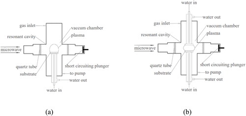
shows the Schematic diagram of different cavity structures. Unlike the traditional single-substrate structure, the upper and lower cavity of the double-substrate structure is symmetrical, and the plasma state can be regulated by adjusting the short-circuiting plunger. In our previous study [Citation27], it has been found that the double-substrate cavity structure can aggregate the plasma at medium and high pressure (10 ∼ 25 kPa). By adopting the double-substrate structure, the radical concentration of Hα, Hβ, C2 and CH can be significantly increased, which is more beneficial for diamond deposition. However, compared with single-substrate structure, the electron temperature of the plasma generated by double-substrate structure is much lower. This is mainly because the average free path of the particles is smaller under high pressure. Meanwhile, the plasma is more concentrated in the double-substrate structure. So the particle motion is more intense, resulting in higher collision frequency. The collisions between electrons and other particles become more frequent, leading to the loss of electron energy and the decrease of electron temperature.
Figure 1. Schematic diagram of MPCVD cavity structure of (a) single-substrate structure and (b) double-substrate structure.
3.1. Effects of different cavity structures on plasma parameters at low pressure
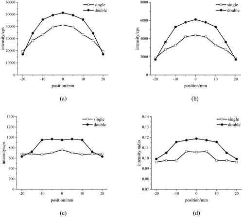
shows the comparison of the spectral intensities of Hα (656.3 nm), Hβ (486.1 nm) and CH (387.1 nm) and the ratio of Hβ to Hα along the horizontal direction in different cavity structures. The measuring range is from -18 mm to 18 mm. It can be seen that the radical strength of the double-substrate structure is significantly higher than that of the single-substrate structure in the range of −10 mm to 10 mm, regardless of Hα, Hβ or CH radicals. Beyond this range, the radical strength of the double-substrate cavity structure decreases sharply. Previous studies have shown that high concentration of Hα radical is more effective in etching the non-diamond phase of carbon, leading to the quality improvement of diamond. The majority of the researchers believe that CH radical is the precursor of the diamond phase [Citation32–34], which plays a very important role in the deposition of diamond films, and the high concentration of CH radical is more favorable for diamond deposition. In addition, the ratio of Hβ to Hα in the double-substrate structure is significantly higher than that in the single-substrate structure. Research shows that the higher the ratio of Hβ to Hα, the higher the electron temperature in the plasma [Citation35]. So the electron temperature in the double-substrate structure at low pressure is higher than that in the single-substrate structure. The main reason for the difference may be that the mean free path of the electrons at low pressure is larger and the collision frequency is smaller. Meanwhile, in contrast with the single-substrate structure, the plasma in the double-substrate structure is more concentrated. Although the electron motion is more intense, the collision frequency does not increase significantly. The electrons still possess a higher energy, thus the electron temperature is higher. The above results show that the double-substrate structure has an aggregation effect on the plasma, which increases the electron temperature of the plasma and the average energy of the collision particles at low pressure. So the active radicals in the plasma is in a highly excited state, which is beneficial to improve the growth rate and quality of diamond.
Figure 2. Horizontal distribution of radicals spectral line intensity in different cavity structures (a) Hα, (b) Hβ, (c) CH, (d) Hβ/Hα.
3.2. Effect of deposition temperatures on diamond growth on GaN layer
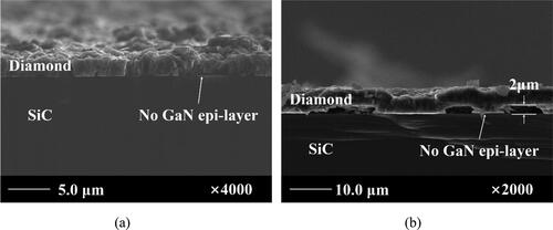
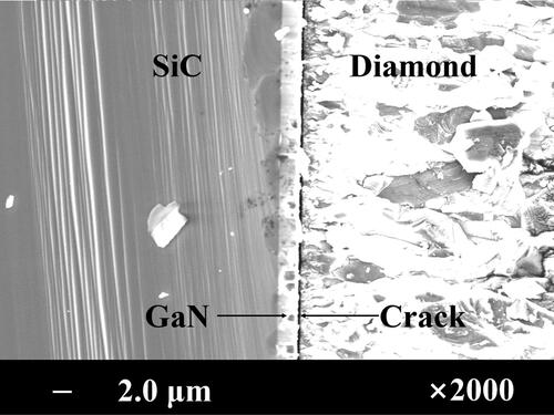
shows the cross-sectional SEM images of diamond deposited directly on GaN epi-layer using a double-substrate structure cavity at 650 °C and 550 °C. It demonstrates that no obvious GaN epi-layer can be found in , and the diamond has been directly deposited on SiC substrate. The 2 μm GaN epi-layer is totally etched by hydrogen plasma when the temperature is higher than 600 °C. As shown in , the GaN epi-layer is also decomposed in hydrogen plasma. Diamond is directly grown on SiC substrate in parts of the interfacial region, while there is a gap of ∼ 2 μm between the SiC substrate and the diamond in the other part. The overall thickness of the diamond is uniform. One possible reason is that the diamond deposition rate is very low at low temperature and low pressure. So the Gann epi-layer is exposed to the hydrogen plasma for a long time during the nucleation process, resulting in the decomposition of GaN epi-layer in parts of the interfacial region. Diamond can grow on the SiC substrate from the very beginning in this region. Moreover, the hydrogen plasma etching during the growth process is isotropic, and the hydrogen plasma will etch the inner wall of the etching pit during the growth process. The GaN epi-layer etching and diamond growth will be carried out at the same time, resulting in a gap between SiC substrate and diamond.
Figure 3. Cross-sectional SEM images of diamond deposited on GaN epi-layer using a double-substrate structure cavity without Si transition layer at (a) 650 °C and (b) 550 °C.
3.3. Effect of thickness of Si transition layer on adhesion of diamond
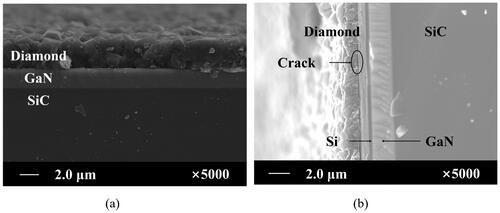
shows the cross-sectional SEM images of diamond deposited on GaN epi-layer using a double-substrate structure cavity at 550 °C with different thickness of Si transition layer. It is shown that when the thickness of the transition layer is 20 nm, the interface between diamond and GaN is clear and sharp, and the 2 μm GaN epi-layer is not etched. When the thickness of the transition layer is 200 nm, the diamond, Si transition layer and GaN epi-layer can be clear observed. However, a visible crack between diamond and Si transition layer can be seen. It is probably because the adhesion between diamond and silicon transition layer is poor, and excessive compressive stress during the cooling process lead to crack generation.
Figure 4. Cross-sectional SEM images of diamond deposited by a double-substrate structure cavity with (a) 20 nm Si buffer layer, 550 °C and (b) 200 nm Si buffer layer, 550 °C.
3.4. Effect of diamond thickness on adhesion
shows the cross-sectional SEM images of 40 μm diamond deposited on GaN epi-layer at 550 °C with 20 nm Si transition layer. It can be seen that the GaN epi-layer is not etched, but the 40 μm diamond is completely separated from the GaN epi-layer. This may be because when the diamond deposition conditions are unchanged, the quality of the top of the diamond film will improve with the increase of the thickness, and the excessive difference between the top and bottom of the diamond will cause the adhesion of the diamond to decrease [Citation36], causing the diamond to shed.
Figure 5. Cross-sectional SEM images of 40 μm diamond deposited on GaN epi-layer at 550 °C with 20 nm Si transition layer.
3.5. Effect of Si transition layer on the quality of diamond
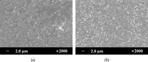
shows the SEM images of the diamond deposited on GaN epi-layer with and without Si transition layer using a double-substrate structure cavity at 550 °C. It can be seen that there are a large number of pinholes in the diamond without Si transition layer, while much less pinholes can be observed in the diamond with Si transition layer. This is likely due to the fact that the decomposition of the GaN epi-layer affects the nucleation and growth of diamond, which leads to the poor denseness of diamond. The presence of the Si transition layer can effectively suppress the etching of GaN by hydrogen plasma, reducing the density of pinholes.
Figure 6. SEM images of the diamond deposited on GaN epi-layer using a double-substrate structure cavity (a) without and (b) with a 20 nm Si transition layer at 550 °C.
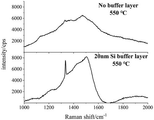
shows the Raman spectra of the diamond deposited on GaN epi-layer using a double-substrate structure cavity with and without Si transition layer at 550 °C. For the diamond with Si transition layer, a strong and sharp peak at ≈1332 cm−1 can be clearly observed, which is generally considered to represent the sp3 hybrid peak of the diamond phase. There are also broad shoulder-like peaks around 1580 cm−1 for both samples. The peak at 1580 cm−1 is considered to represent the sp2 hybrid peak (G peak) of the non-diamond phase. The intensity ratios Isp3/Isp2 of the sample with 20 nm Si transition layer is significantly larger, indicating that the existence of 20 nm transition layer improves the quality of diamond deposited on GaN epi-layer.
Figure 7. Raman spectra of the diamond deposited on GaN epi-layer using a double-substrate structure cavity with and without Si transition layer at 550 °C.
4. Conclusion
In summary, diamond film with a Si transition layer has been successfully deposited on GaN epi-layer by a homemade double-substrate structure MPCVD at low temperature and low pressure. Plasma emission diagnostics show that compared with the single-substrate structure, the plasma in the double-substrate structure MPCVD is more concentrated. The electron temperature and active radical concentration in the double-substrate structure at low pressure is higher than that in the single-substrate structure, leading to the quality improvement of diamond. The decomposition of GaN epi-layer in hydrogen plasma is significantly suppressed by introducing a Si transition layer. With an optimum Si transition layer of 20 nm, the quality of the diamond can be effectively improved. However, the Si transition layer with excessive thickness will lead to the generation of cracks between diamond and transition layer. An excessively thick diamond film will also lead to a decrease in adhesion, and it is necessary to increase the adhesion of diamond to deposit a thick diamond film on the GaN epi-layer. The results demonstrated in this paper provide a new approach to prepare diamond film on GaN epi-layer.
Disclosure statement
No potential conflict of interest was reported by the author(s).
Reference
- Mishra UK, Parikh P, Wu Y-F. AlGaN/GaN HEMTs-an overview of device operation and applications. Proc. IEEE. 2002;90(6):1022–1031.
- Kanamura M, Ohki T, Kikkawa T, et al. Recent progress in GaN HEMT for high-frequency and high-power applications; Proceedings of the 2012 IEEE International Symposium on Radio-Frequency Integration Technology (RFIT), 2012. IEEE.
- Ejeckam F, Francis D, Faili F, et al. S2-T1: GaN-on-diamond: A brief history; Proceedings of the 2014 Lester Eastman Conference on High Performance Devices (LEC), 2014. IEEE.
- Ishizaki T, Yanase M, Kuno A, et al. Thermal simulation of joints with high thermal conductivities for power electronic devices. Microelectron Reliab. 2015;55(7):1060–1066.
- Ohno Y, Kuzuhara M. Application of GaN-based heterojunction FETs for advanced wireless communication. IEEE Trans. Electron Devices. 2001;48(3):517–523.
- Boutros KS, Chu R, Hughes B. GaN power electronics for automotive application; Proceedings of the 2012 IEEE Energytech, 2012. IEEE.
- Muraro J-L, Nicolas G, Forestier S, et al. GaN for space application: almost ready for flight. Int J Microw Wirel Technol. 2010;2(1):121–133.
- Zhang L, Wang S, Shao Y, et al. One-step fabrication of porous GaN crystal membrane and its application in energy storage. Sci Rep. 2017;7(1):1–9.
- Gaska R, Osinsky A, Yang J, et al. Self-heating in high-power AlGaN-GaN HFETs. IEEE Electron Device Lett. 1998;19(3):89–91.
- Filippov K, Balandin A. The effect of the thermal boundary resistance on self-heating of AlGaN/GaN HFETs. Mater Res Soc Internet J Nitride Semicond Res. 2003;8:4.
- Francis D, Wasserbauer J, Faili F, et al. GaN-HEMT epilayers on diamond substrates: recent progress. 2007.
- Shibata H, Waseda Y, Ohta H, et al. High thermal conductivity of gallium nitride (GaN) crystals grown by HVPE process. Mater Trans. 2007;48(10):2782–2786.
- Wei R, Song S, Yang K, et al. Thermal conductivity of 4H-SiC single crystals. J Appl Phys. 2013;113(5):053503.
- Singhal S, Li T, Chaudhari A, et al. Reliability of large periphery GaN-on-Si HFETs. Microelectron Reliab. 2006;46(8):1247–1253.
- Wort C, Sweeney C, Cooper M, et al. Thermal properties of bulk polycrystalline CVD diamond. Diamond Relat Mater. 1994;3(9):1158–1167.
- Sang L. Diamond as the heat spreader for the thermal dissipation of GaN-based electronic devices. Functional Diamond. 2021;1(1):174–188.
- Cheng Z, Mu F, Yates L, et al. Interfacial thermal conductance across room-temperature-bonded GaN/diamond interfaces for GaN-on-diamond devices. ACS Appl Mater Interfaces. 2020;12(7):8376–8384.
- Liang J, Kobayashi A, Shimizu Y, et al. Fabrication of GaN/diamond heterointerface and interfacial chemical bonding state for highly efficient device design. Adv Mater. 2021;33(43):2104564.
- Chernykh M, Andreev A, Ezubchenko I, et al. GaN-based heterostructures with CVD diamond heat sinks: a new fabrication approach towards efficient electronic devices. Appl Mater Today. 2022;26:101338.
- Ahmed R, Siddique A, Anderson J, et al. Integration of GaN and diamond using epitaxial lateral overgrowth. ACS Appl Mater Interfaces. 2020;12(35):39397–39404.
- Soleimanzadeh R, Naamoun M, Floriduz A, et al. Seed dibbling method for the growth of high-quality diamond on GaN. ACS Appl Mater Interfaces. 2021;13(36):43516–43523.
- Mandal S, Thomas EL, Middleton C, et al. Surface zeta potential and diamond seeding on gallium nitride films. ACS Omega. 2017;2(10):7275–7280.
- Xin J. Study on preparation and properties of GaN foundation corundum heat dissipation layer. University of Science and Technology Beijing, 2020.
- Ahmed R, Siddique A, Anderson J, et al. Selective area deposition of hot filament CVD diamond on 100 mm MOCVD grown AlGaN/GaN wafers. Cryst Growth Des. 2019;19(2):672–677.
- Graebner J, Jin S, Kammlott G, et al. Large anisotropic thermal conductivity in synthetic diamond films. Nature. 1992;359(6394):401–403.
- May PW, Tsai HY, Wang WN, et al. Deposition of CVD diamond onto GaN. Diamond Relat Mater. 2006;15(4–8):526–530.
- Kangjun D, Zhibin M, Hongwei H, et al. Novel reactor with double substrate holders for microwave plasma chemical vapor deposition. Chin J Vacuum Sci Technol. 2017;37(5):488.
- Malakoutian M, Ren C, Woo K, et al. Development of polycrystalline diamond compatible with the latest N-Polar GaN mm-Wave technology. Cryst Growth Des. 2021;21(5):2624–2632.
- Zhou Y, Ramaneti R, Anaya J, et al. Thermal characterization of polycrystalline diamond thin film heat spreaders grown on GaN HEMTs. Appl Phys Lett. 2017;111(4):041901.
- Yates L, Anderson J, Gu X, et al. Low thermal boundary resistance interfaces for GaN-on-diamond devices. ACS Appl Mater Interfaces. 2018;10(28):24302–24309.
- Kuwabara A, Matsunaga K, Tanaka I. Lattice dynamics and thermodynamical properties of silicon nitride polymorphs. Phys Rev B. 2008;78(6):064104.
- Liping T. Spectral analysis of diamond films deposited by MPCVD. Wuhan Institute of Technology, 2013.
- Mitsuda Y, Kojima Y, Yoshida T, et al. The growth of diamond in microwave plasma under low pressure. J Mater Sci. 1987;22(5):1557–1562.
- Balestrino G, Marinelli M, Milani E, et al. Growth of diamond films: general correlation between film morphology and plasma emission spectra. Appl Phys Lett. 1993;62(8):879–881.
- Rong WU, Yan LI, Shun-Guan ZHU, et al. Emission spectroscopy diagnostics of plasma electron temperature. Spectrosc Spectral Anal. 2008;4:731–735.
- Lei X, Wang L, Shen B, et al. Microdrill with variations in thickness of diamond coating. Surf Eng. 2016;32(3):165–171.