
 ?Mathematical formulae have been encoded as MathML and are displayed in this HTML version using MathJax in order to improve their display. Uncheck the box to turn MathJax off. This feature requires Javascript. Click on a formula to zoom.
Abstract
In recent years, diamond has shown great potential in solar-blind ultraviolet (UV) photodetection due to its ultrawide bandgap (∼ 5.5 eV) and other superior semiconductor properties. However, the response region of diamond photodetector is usually smaller than 230 nm, which cannot cover the whole solar-blind region from 200 to 280 nm. In this work, an ε-Ga2O3/diamond photodetector with wide spectra responsivity from 210 (or even lower) to 260 nm was fabricated. High-quality ε-Ga2O3 film with columnar crystal was epitaxially grown on single crystalline CVD diamond substrate by pulse laser deposition (PLD). TEM characterization revealed that the ε-Ga2O3 film grew along the <001> orientation on diamond (100) substrate. The deep ultraviolet (DUV) photodetector based on the ε-Ga2O3/diamond structure showed a high light-to-dark ratio over 5.7 × 10⁴ and good linear response to the incident light power density from 10 to 400 mW/cm2. Moreover, compared to other photodetectors, the fabricated ε-Ga2O3/diamond photodetector achieved high responsivity and wide spectra response region from 210 to 260 nm, with high solar-blind rejection ratio of 104 (R240/R280) and 165 (R210/R280), respectively. The extension of spectra region with high responsivity of the ε-Ga2O3/diamond photodetector can be attributed to the thin thickness of ε-Ga2O3 film (around 200 nm) and parts of the DUV light were absorbed by diamond. The high responsivity and wide spectra response region indicate the fabricated ε-Ga2O3/diamond photodetector can be used for the detection of ultraviolet in the most of the DUV region.
1. Introduction
The deep ultraviolet (DUV) with wavelengths from 200 to 280 nm is commonly referred to as the solar-blind UV range, as solar radiation in this wavelength region is effectively blocked by the ozone layer in the Earth’s atmosphere [Citation1–3]. Owing to the low natural background, photodetectors operating in solar-blind region have high signal-to-noise ratios and low false alarm rates. Therefore, solar-blind photodetectors have many civil and military applications such as biological/chemical, sterilization and disinfection, missile tracking and environmental monitoring [Citation4–6]. Unfortunately, most of the commercial semiconductor DUV photodetectors are made of silicon (Si), and the narrow bandgap (1.12 eV) makes Si photodetector vulnerable to visible light interference during DUV detection, thus limiting its applications. Diamond has emerged as a promising material for solar-blind photodetection due to its wide bandgap (Eg: ∼ 5.5 eV) and high radiation hardness, which can promise intrinsic invisible/solar blindness [Citation7,Citation8]. However, due to the limitation of the band gap and UV adsorption edge, diamond photodetectors only show response to DUV light with wavelengths smaller than 230 nm. Therefore, to realize the full (or nearly full) wavelength and high response to DUV light in a single photodetector, a semiconductor with smaller bandgap is necessarily to be employed to form heterostructure with diamond.
Gallium oxide (Ga2O3), as another ultrawide bandgap semiconductor, has also been widely used for DUV photodetection due to its wide bandgap (Eg: ∼ 4.9 eV), and other fantastic physical and electrical properties [Citation9,Citation10]. However, due to the decrease of adsorption coefficient (α) in the short wavelength region (< 240 nm) [Citation11,Citation12], the high spectra response regions of the Ga2O3 photodetectors are usually between 240 and 260 nm [Citation13–15], which correspond exactly to the irresponsive region of diamond photodetectors in DUV region. Therefore, the combination of Ga2O3 and diamond has gained much interest in recent years, leading to the development of different fabrication methods of Ga2O3/diamond photodetectors [Citation16,Citation17]. Kim et al. transferred the β-Ga2O3 nanolayer onto the diamond substrate through mechanical exfoliation and fabricated a β-Ga2O3/diamond photodetector [Citation16]. However, the fragility of β-Ga2O3 film limits the transferring of large-scale β-Ga2O3 films. Therefore, Chen et al. fabricated a β-Ga2O3/diamond photodetector by growing β-Ga2O3 film on diamond substrate through plasma enhanced chemical vapor deposition (PECVD) [Citation17]. However, due to the low symmetric monoclinic structure of β-Ga2O3 (space group: C2/m) and lattice mismatch between β-Ga2O3 and diamond, the β-Ga2O3 film had a poor crystalline quality with a full width at half maximum (FWHM) of the rocking curve of over 2°, which leaded to a low responsivity (0.2 mA/W).
As another major Ga2O3 polymorph, ε-Ga2O3 is the second most stable phase and has many fantastic properties, like ferroelectric polarization [Citation18,Citation19]. Recently, the crystal structure of ε-Ga2O3 has been demonstrated to be composed of orthogonal nanoscale (about 5–10 nm) ordered κ-Ga2O3 cells (space group: Pna21) arranged 120° next to each other [Citation20]. Therefore, the crystal structure of ε-Ga2O3 is regarded as orthographic (space group: Pna21) rather than the hexagonal (space group: P63mc) as previously thought. The orthorhombic crystal structure promises ε-Ga2O3 more suitable for epitaxial growth on hexagonal and cubic semiconductor substrates [Citation21–23]. Therefore, due to better lattice compatibility, the high crystallographic symmetry indicates that it is possible to grow high quality ε-Ga2O3 crystal on single crystalline diamond substrates. In our previous work, an ε-Ga2O3/diamond photodetector with high thermal stability was fabricated by growing crystalline ε-Ga2O3 film on the diamond substate [Citation24]. However, till now, there are few reports on the epitaxial growth of ε-Ga2O3 on diamond substrate, as well as the photodetector based on ε-Ga2O3/diamond heterostructure.
In this work, an ε-Ga2O3/diamond photodetector with nearly full spectra response in DUV region was fabricated. The high quality ε-Ga2O3 film was epitaxially grown on single crystalline diamond substrate by pulsed laser deposition (PLD). The crystal qualities of the ε-Ga2O3 film on the diamond substrate were detailly characterized by XRD and TEM, which revealed that the ε-Ga2O3 film was composed of a series of columnar crystals with in-plane rotational domains. Besides, the detailed structure of ε-Ga2O3/diamond interface was determined by a combination of high-resolution scanning TEM and first principles calculations. Based on the obtained ε-Ga2O3/diamond heterostructure, a DUV photodetector was fabricated by depositing Ti/Au electrodes on ε-Ga2O3 surface. Compared to other Ga2O3 photodetectors, the fabricated ε-Ga2O3/diamond photodetector showed high spectra response from below 210 nm to the wavelength about 260 nm. The fabrication of ε-Ga2O3/diamond photodetector with broad and high spectra response will push the investigation of the integration of ultrawide bandgap heterostructures in the future.
2. Materials and experiments
The CVD diamond (100) substrate with size of 7 × 7 × 0.3 mm3 used in this work is grew in our lab by micro-plasma chemical vapor deposition (MPCVD). The Raman peak center of the CVD diamond locates at about 1332.3 cm−1 and the full width at half maximum (FWHM) is about 2.1 cm−1. The ε-Ga2O3 film was deposited on diamond substrate by PLD system (SKY Technology Development Co., Ltd. Chinese Academy of Science) using a 248 nm KrF excimer laser. During ε-Ga2O3 growth, the oxygen pressure and growth temperature were maintained at 20 mTorr and 800 °C, respectively. The thickness of ε-Ga2O3 film can be controlled by changing the deposition cycling times. An ε-Ga2O3/diamond photodetector with metal-semiconductor-metal (MSM) structural interdigital electrodes (200 μm gap between electrodes) was then fabricated by depositing Ti (30 nm)/Au (50 nm) on the grown ε-Ga2O3 surface through electron beam deposition system (SKY Technology Development Co., Ltd. Chinese Academy of Science). An in-situ thermal annealing at about 450 °C was performed in vacuum to achieve good Ohmic contact between electrodes and substrate.
The crystal structure of ε-Ga2O3 film grown on single crystalline diamond substrate was characterized by X-ray diffraction (XRD, D8 Advance, Bruker, USA), and the microstructure of the ε-Ga2O3 film was characterized using an aberration-corrected transmission electron microscopy (TEM, Spectra 300, Themo Fisher Scientific, USA). The transmittance of ε-Ga2O3, diamond and ε-Ga2O3/diamond samples in the range from 190 to 800 nm were measured by UV-Visible spectrometer (Lambda 1050+, Perkin Elmer, USA). The I–V characteristic of the ε-Ga2O3/diamond photodetector was measured in a semiconductor parameter analyzer (Keithley 4200-SCS, Tektronix, USA) under the illumination of different ultraviolet light sources. For the scanning test, the voltage was increased from minus to positive values at a step of 0.2 V. The UV source used in this work is composed of a while light source (EQ99X LDLS, Energetiq, Holland) and spectrophotometer (iHR 320, Horiba, Japan).
3. Results and disscussion
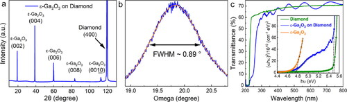
XRD was performed to characterize the crystal phase and orientation of the as-grown Ga2O3 film on diamond substrate. According to the θ–2θ scan in , besides the (400) plane diffraction peak of diamond substrate located at 119.4°, five obvious diffraction peaks at 19.1°, 38.8°, 59.8°, 83.5° and 112.7° can be also observed, which belong to the (002), (004), (006), (008) and (0010) planes of ε-Ga2O3 (space group: Pna21) [Citation20]. The appearance of the only (001) series diffraction peaks of ε-Ga2O3 on the XRD spectra confirms that the as-grown ε-Ga2O3 film on diamond substrate has high purity and high crystal orientation. As shown in , the measured FWHM of the ε-Ga2O3 (002) in the ω-scan mode is about 0.89°, which is much lower than the reported β-Ga2O3 film on diamond substrate grown by low pressure chemical vapor deposition (LPCVD) [Citation25]. shows the comparison of the transmittance of diamond sample in the UV-visible region before and after ε-Ga2O3 film deposition. The transmittance of diamond is around 70% in the visible region, approximating to the theoretical value of intrinsic diamond. After ε-Ga2O3 deposition, when light is transmitted from ε-Ga2O3 side, the transmittance of ε-Ga2O3/diamond sample is limited below 70% in the region from 300 to 800 nm due to the existence of diamond substrate. Moreover, two absorption edges at 275 nm and 228 nm can be observed, which belong to the absorption edges of intrinsic ε-Ga2O3 film and diamond substrate, respectively. The insert Tauc plot analysis in revels that optical bandgap of ε-Ga2O3 film and diamond substrate are about 4.8 and 5.5 eV, respectively. The transmittance comparisons of the ε-Ga2O3/diamond samples with different ε-Ga2O3 thicknesses are shown in Figure S1 in Supplementary Information. With the increase of ε-Ga2O3 film thickness from about 10–200 nm, the transmittances of ε-Ga2O3/diamond samples, where the absorption edge of diamond occurred, decreased from about 40% to 8%. When thickness of ε-Ga2O3 is higher than 400 nm, the DUV below 230 nm is fully adsorbed by ε-Ga2O3 film, as shown in Figure S1.
Figure 1. (a) XRD θ-2θ scan of ε-Ga2O3 film grown on diamond substrate, (b) XRD ω-scan of around the ε-Ga2O3 (002) peak, (c) comparison of the UV-Vis transmittance spectra and Tauc plot (Inset) of ε-Ga2O3 film grown on diamond substrate (blue), diamond (green) and ε-Ga2O3 (orange). the thickness of ε-Ga2O3 film in (c) is about 225 nm.
The microstructure of ε-Ga2O3 film on diamond substrate was characterized by TEM, as shown in . It can be seen from the low magnification cross-section TEM image shown in that the thickness of ε-Ga2O3 film is around 200 nm. The ε-Ga2O3 film shows a lath-shaped contrast vertical to the surface of diamond substrate, indicating the grown ε-Ga2O3 film is polycrystalline composing of columnar structures, which was further verified by the selected area electron diffraction (SAED) pattern and high-resolution TEM (HRTEM) image, shown in and . The main diffraction spots (circled by green circles) in the SAED pattern shown in can be attributed to the ε-Ga2O3 grain oriented along the [010] zone axis, while other diffraction spots are attributed to the in-plane domain rotations of the ε-Ga2O3 crystal lattice (Figure S2 in supporting information). It is worth noting that all diffraction spots observed in the SAED formed lines perpendicular to the [001] crystallographic direction, indicating that the (001) planes of all ε-Ga2O3 grains are parallel to each other, and it is consistent with the XRD pattern showing high orientation consistency of the as-grown ε-Ga2O3. shows an HRTEM image of the ε-Ga2O3 containing two grains separated by the grain boundary marked in green. The interplanar spacings for both grains are determined to be 0.93 nm, which is consistent with the value expected for the (001) crystal planes of ε-Ga2O3 [Citation20]. Due to the parallel alignment of the (001) crystal planes of ε-Ga2O3 with the diamond substrate, the perpendicular orientation of the grain boundary (marked by a green line) to the (001) planes of the two adjacent grains indicates the columnar crystal structure of the ε-Ga2O3 and also confirms the consistent orientation of the grains along the <001> direction. Scanning TEM (STEM) was carried out on the ε-Ga2O3 grain with [010] zone axis, as shown in . The structure of the grain is consistent with the crystal model of ε-Ga2O3 viewed along the [010] direction as shown in , confirming again the ε-phase of Ga2O3 on diamond substrate.
Figure 2. (a) Low magnification cross-section TEM image of ε-Ga2O3 film on diamond. (b) SEAD pattern taken from the region marked by the dashed circle in (a). (c) HRTEM image showing the grain boundary in the ε-Ga2O3 film. (d) STEM image showing the ε-Ga2O3 structure with the [010] zone axial at atomic resolution. (e) Enlarged image taken from the yellow rectangular region of (d). the insert in (e) shows the atomic model of ε-Ga2O3 viewed along the [010] direction. The red and blue balls represent Ga and O atoms, respectively.
![Figure 2. (a) Low magnification cross-section TEM image of ε-Ga2O3 film on diamond. (b) SEAD pattern taken from the region marked by the dashed circle in (a). (c) HRTEM image showing the grain boundary in the ε-Ga2O3 film. (d) STEM image showing the ε-Ga2O3 structure with the [010] zone axial at atomic resolution. (e) Enlarged image taken from the yellow rectangular region of (d). the insert in (e) shows the atomic model of ε-Ga2O3 viewed along the [010] direction. The red and blue balls represent Ga and O atoms, respectively.](/cms/asset/950ef8df-de92-484b-9094-25ca4f27ae03/tfdi_a_2256360_f0002_c.jpg)
In order to understand the growth mechanism of ε-Ga2O3 on diamond substrate, the microstructure of ε-Ga2O3/diamond interface was investigated by a combination of TEM characterizations and first principles calculations. The STEM image of the ε-Ga2O3/diamond interface is shown in where the (001) planes of ε-Ga2O3 are parallel to the (001) planes of diamond. It can also be observed that there is not an obvious interface layer between diamond and ε-Ga2O3 crystal. The suitable epitaxial growth of ε-Ga2O3 on substrates with cubic and orthorhombic structures is due to the orthorhombic structure of ε-Ga2O3. It should be noted that the lattice constant aε of ε-Ga2O3 is 5.04 Å [Citation20], which is very close to the facial diagonal length of the unit cell of cubic diamond: aD = 5.01 Å. The lattice constant mismatch between aε and
aD is smaller than 1%. However, for the lattice constant bε of ε-Ga2O3, it follows: 3/2
aD < bε < 2
aD, as shown in Figure S3 in Supplementary Information. Therefore, beside of 120°, other rotation angles may occur during ε-Ga2O3 growth, while the pseudohexagonal 4H stacking of the O atoms is preserved, giving rise of the columnar structure of ε-Ga2O3 on diamond substrate [Citation20]. The SAED pattern taken from the ε-Ga2O3/diamond interface is shown in . The reflections of diamond marked by green circles and ε-Ga2O3 marked by yellow circles show that the (001) planes of the ε-Ga2O3 are parallel to the (001) planes of diamond, which matches well with the HRTEM image shown in .
Figure 3. (a) STEM image of the ε-Ga2O3/diamond interface. (b) SAED pattern taken from the ε-Ga2O3/diamond interface. Diffraction spots marked by green and yellow circles represent diamond (with [110] zoon axis) and ε-Ga2O3 (with [010] zoon axis), respectively. (c) Atomic model of the ε-Ga2O3/diamond interface. The red and blue balls represent Ga and O atoms. The green and white balls represent the C atoms at the surface and inner of diamond substrate, respectively. (d) The calculated total energies of different atomic layers of ε-Ga2O3 contacting with (001) diamond substrate.
![Figure 3. (a) STEM image of the ε-Ga2O3/diamond interface. (b) SAED pattern taken from the ε-Ga2O3/diamond interface. Diffraction spots marked by green and yellow circles represent diamond (with [110] zoon axis) and ε-Ga2O3 (with [010] zoon axis), respectively. (c) Atomic model of the ε-Ga2O3/diamond interface. The red and blue balls represent Ga and O atoms. The green and white balls represent the C atoms at the surface and inner of diamond substrate, respectively. (d) The calculated total energies of different atomic layers of ε-Ga2O3 contacting with (001) diamond substrate.](/cms/asset/513e6c1a-ba2d-48fd-820b-ea4c92ee0fdf/tfdi_a_2256360_f0003_c.jpg)
The crystal structure of ε-Ga2O3 is complex, whose unit cell contains 16 Ga and 24 O atoms. The atoms in one unit cell can be clarified into 10 different layers vertical to the [001] direction. Thanks to the high-resolution STEM image, the atomic model of the ε-Ga2O3/diamond interface is shown in . The atomic layers of ε-Ga2O3 are labeled as 1–10. One should be aware that it is difficult to determine the atomic layer close to the diamond by TEM characterizations due to its limited resolution. In this case, the first principle calculation was used to analyze the detailed structure of the ε-Ga2O3/diamond interface. The ε-Ga2O3/diamond interface models containing 140 atoms (96 C atoms, 17 Ga atoms and 27 O atoms) were built for calculations. A vacuum space of 12 Å was left along the Z-direction. The calculation was carried out using the Vienna ab initio Simulation Package (VASP) based on density functional theory, and the Projector-Augmented Wave (PAW) method together with the Perdew Burke Ernzerhof (PBE) formulation were employed [Citation26]. The cutoff energy of the plane waves was set as 450 eV and the Monkhorst-Pack K-point mesh was 4 × 4 × 1. The diamond structure was fixed and the ε-Ga2O3 structure was fully relaxed until the Hellmann-Feynman force on all atoms was less than 0.05 eV/Å. The calculated total energy of the ε-Ga2O3/diamond interface system is shown in . The total energy varies from −986 eV to −980 eV when the O atoms of ε-Ga2O3 contact with diamond substrate, lower than that when the Ga atoms of ε-Ga2O3 contact with diamond substrate (−973 eV to −962 eV). The calculated results show that compared to Ga atoms, the C atoms on diamond surface tend to form covalent bonds with O atoms due to the closer covalent radiuses of C (0.77 Å) and O (0.73 Å) atoms.
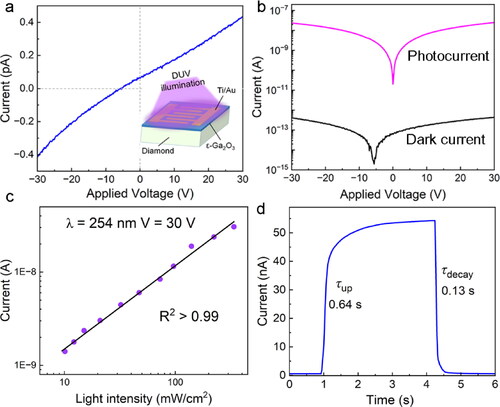
A solar-blind photodetector based on the obtained ε-Ga2O3/diamond heterostructure was fabricated by depositing Ti (30 nm)/Au (50 nm) interdigital electrodes on ε-Ga2O3 surface. As shown in , the measured I–V curve was almost linear under no light illumination which indicates a good ohmic contact of Ti/Au electrodes on ε-Ga2O3 surface. The zero point of the I–V curve shifted to the negative voltage because of charging and discharging on the highly insulating ε-Ga2O3 film. At an applied voltage of 30 V, the ultralow dark current was about 4.3 × 10⁻¹³ A as shown in . When exposed to 240 nm ultraviolet light, the ε-Ga2O3/diamond photodetector (effective area: ∼ 2.2 mm2) achieved a photocurrent of about 2.5 × 10⁻⁸ A for an applied bias of 30 V and a light-to-dark current ratio of more than 5.7 × 10⁴. The photoresponse of ε-Ga2O3/diamond photodetector under different incident light power densities is shown in where the photocurrent shows a linear relationship to the incident light power density from 10 mW/cm2 to over 400 mW/cm2. Moreover, the time response of the ε-Ga2O3/diamond photodetector is shown in . The measured rise time (τup) and decay time (τdecay) of the photodetector are about 0.64 s and 0.13 s when the current increases from 10% to 90% and decreases from 90% to 10% of the maximum current, respectively. The rise and decay times of the photodetector are similar to the reported values of other Ga2O3/diamond photodetectors [Citation17,Citation24].
Figure 4. (a) The I–V curve of the ε-Ga2O3/diamond photodetector, the insert is the schematic illustration of the fabricated ε-Ga2O3/diamond photodetector. (b) Photocurrent and dark current of the ε-Ga2O3/diamond photodetector. (c) Relationship of the photo response to the incident light power density. (d) Time response of the fabricated ε-Ga2O3/diamond photodetector.
The spectra response of the ε-Ga2O3/diamond photodetector under different ultraviolet wavelength is shown in . As shown in , with the decrease of incident ultraviolet wavelength, the photocurrent increased dramatically. Notably, the zero point shift disappeared on the I–V curves when the ε-Ga2O3/diamond photodetector was illuminated to the DUV light with wavelength smaller than 260 nm. It can be explained that when the illumination DUV wavelength was smaller than 260 nm, photocurrent would be generated in the ε-Ga2O3 layer and the photo-generated carrier balanced the defects in ε-Ga2O3 layer, leading to the disappearance of the zero point shift. The calculated responsivity is shown in , in which the insert shows the logarithmic relationship of the responsivity of the ε-Ga2O3/diamond photodetector to incident wavelength at different applied voltages. For independent Ga2O3 and diamond photodetectors, the peak responsivity usually locates at around 250 and 225 nm, respectively. However, in this work, the responsivity of the ε-Ga2O3/diamond photodetector did not reduce like other ε-Ga2O3 photodetectors, when the incident wavelength decreased to 240 nm [Citation27,Citation28]. Instead, a second increase tendency can be observed on the responsivity curve when the ultraviolet wavelength decreased below 230 nm. When the ultraviolet wavelength decreased to 210 nm, the responsivity achieved the maximum value of 0.28 A/W for voltage of 30 V. The high spectra responsivity region of ε-Ga2O3/diamond photodetector (ε-Ga2O3: ∼200 nm) was extended to 260–210 nm or even lower. While for an ε-Ga2O3/diamond photodetector with 1 μm- thick ε-Ga2O3 film, as shown in Figure S4, the peak responsivity of the ε-Ga2O3/diamond photodetector locates at around 250 nm, and with the decrease of illumination wavelength from 250 nm, the responsivity decreased dramatically, which was also reported in Ref. [Citation24].
Figure 5. (a) Photocurrent and (b) responsivity of ε-Ga2O3/diamond photodetector under different incident wavelength ultraviolet light at different applied voltage, the insert figure in (b) shows corresponding logarithmic responsivity. The (c) solar-blind and (d) visible rejection ratio of the ε-Ga2O3/diamond photodetector at different applied voltages, respectively. A schematic illustration of the electric field intensity in ε-Ga2O3/diamond photodetector with (e) 200 nm and (f) 1 μm ε-Ga2O3 layer.
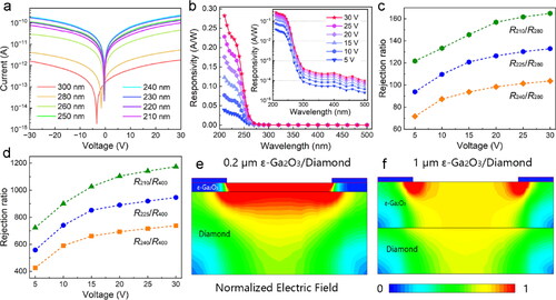
Moreover, show the solar-blind and visible light rejection ratios of the ε-Ga2O3/diamond photodetector under different applied voltages. It can be observed that all the rejection ratio curves show an increase tendency to the applied voltage from 5 V to 30 V. With the decrease of ultraviolet wavelength, the solar-blind rejection ratios of the ε-Ga2O3/diamond photodetector increases from 104 (R240/R280) to 133 (R225/R280) and 165 (R210/R280) at 30 V, respectively. Meanwhile, the visible light rejection ratios increase from 738 (R240/R280) to 946 (R225/R280) and 1174 (R210/R280) at 30 V, respectively. Such rejection values are much higher than the reported values of other Ga2O3/diamond photodetectors [Citation17,Citation24]. The high solar-blind and visible-blind rejection ratios of the ε-Ga2O3/diamond photodetector indicate the good solar-blind properties of the proposed ε-Ga2O3/diamond photodetector. Moreover, compared to the Ga2O3/diamond photodetectors in Figure S4 and other reports, the wavelength response region of the proposed ε-Ga2O3/diamond photodetector extended from 230 nm to below 210 nm, which was never reported before. Considering the occurrence of two adsorption edges of ε-Ga2O3/diamond in the UV-Vis spectra in , the wide spectra responsivity of the fabricated ε-Ga2O3/diamond photodetector is due to the ultraviolet response of diamond substrate.
The simulation of the optical intensity and electric field distribution in ε-Ga2O3/diamond photodetector with different ε-Ga2O3 thickness were performed and compared. According to traditional physical theory, the light intensity decays exponentially with the light penetration depth. When the ε-Ga2O3 film was 200 nm or thinner, the DUV light can transmit the ε-Ga2O3 layer to the diamond substrate, which will generate the photocurrent in the diamond substrate (Figure S5). However, with the increase of ε-Ga2O3 film thickness, nearly all the DUV light with wavelength smaller than 230 nm was adsorbed by the ε-Ga2O3 layer, leading to the small or little photocurrent in diamond. Moreover, the distribution of the electric field in ε-Ga2O3 and diamond layers also reveal that with the increase of ε-Ga2O3 thickness, the electric field intensity becomes weaker in the diamond substrate, as shown in and Figure S6. Besides the above two reasons, quantum efficiency is also an important influence factor. The single crystalline diamond has much higher quantum efficiency than the columnar crystalline ε-Ga2O3 layer in the DUV region. Therefore, the extension of the spectra response region of the ε-Ga2O3/diamond photodetector was caused by above many reasons. The wide spectra response region indicates the ε-Ga2O3/diamond photodetector can be used for photodetection in the most of the DUV region.
4. Conclusion
In this work, an ε-Ga2O3/diamond photodetector with high spectra responsivity through the region from 210 nm to 260 nm was fabricated by epitaxially depositing ε-Ga2O3 film on diamond substrate by PLD. The microstructure of ε-Ga2O3 film gown on diamond has been shown to be the columnar crystal that rotating along the z axis. Due to the better lattice compatibility and crystal matching of ε-Ga2O3 and diamond, the ε-Ga2O3 film has good crystal quality with the FWHM of the ε-Ga2O3 (002) rocking curve of 0.89°. In comparison to other independent photodetectors based on ε-Ga2O3 or diamond materials, the fabricated ε-Ga2O3/diamond heterojunction photodetector achieved a significantly wide spectra response, from below 210 nm to about 260 nm. Moreover, the high rejection ratios for the responsivity for wavelengths of 280 nm and 400 nm were obtained, which demonstrated a high selectivity and sensitivity of the ε-Ga2O3/diamond photodetector in the most of the DUV region. The high responsivity and wide spectra region of the ε-Ga2O3/diamond photodetector shows great potential applications in DUV detection.
5. Associated content
Supporting Information: (I) Comparison of the UV-visible transmittance of ε-Ga2O3/diamond samples with different ε-Ga2O3 thicknesses. (II) The diffraction spots in the SAED pattern of ε-Ga2O3 film. (III) A potential contacting model of ε-Ga2O3 on diamond substrate according to calculation. (IV) The photo responsivity of the ε-Ga2O3/diamond photodetector with thick ε-Ga2O3 film. (V) Comparison of the optical intensity in ε-Ga2O3/diamond photodetector. (VI) Comparison of the electric field in ε-Ga2O3/diamond photodetector.
Author contributions
Q. Y.: conceived, measured photoresponse and wrote the manuscript; W. W.: grew ε-Ga2O3 film; W. Z.: gave direction on the ε-Ga2O3 growth; M. Q.: fabricated the device; M. Y. and Z. J.: helped measure photoresponse, B. W.: performed TEM characterization, C.-T. L. and K. N.: supervised the project; K. C.: developed the simulation; K. W. A. C.: supervised and corrected the manuscript; J. C.: TEM analysis and developed the theoretical model; N. Jiang: supervised and corrected the manuscript. All authors contributed to the discussions.
Supplemental Material
Download MS Word (977.3 KB)Acknowledgements
The authors thank Bingxue Zhang and Mingxin Hao (Qianwan Institute of CNITECH) for assistance with the characterization of ultraviolet-visible (UV-Vis) spectrophotometer and TEM sample preparation.
Disclosure statement
No potential conflict of interest was reported by the authors.
Additional information
Funding
Reference
- Xie C, Lu X-T, Tong X-W, et al. Recent progress in solar-blind deep-ultraviolet photodetectors based on inorganic ultrawide bandgap semiconductors. Adv Funct Mater. 2019;29:1.
- Qin Y, Long SB, Dong H, et al. Review of deep ultraviolet photodetector based on gallium oxide. Chinese Phys B. 2019;28(1):018501.
- Lu YJ, Lin CN, Shan CX. Optoelectronic diamond: growth, properties, and photodetection applications. Adv Optical Mater. 2018;6(20):1800359.
- Varshney U, Aggarwal N, Gupta G. Current advances in solar-blind photodetection technology: using Ga2O3 and AlGaN. J Mater Chem C. 2022;10(5):1573–8.
- Cai Q, You HF, Guo H, et al. Progress on AlGaN-based solar-blind ultraviolet photodetectors and focal plane arrays. Light Sci Appl. 2021;10:94.
- Hu X, Li XY, Li GY, et al. Recent progress of methods to enhance photovoltaic effect for self-powered heterojunction photodetectors and their applications in inorganic low-dimensional structures. Adv Funct Mater. 2021;31:2011284.
- Liu Z, Zhao D, Zhu T, et al. Enhanced responsivity of diamond UV detector based on regrown lens structure. IEEE Electron Device Lett. 2020;41(12):1829–1832.
- Lin CN, Lu YJ, Yang X, et al. Diamond-based all-carbon photodetectors for solar-blind imaging. Adv Optical Mater. 2018;6:1800068.
- Guo D, Guo Q, Chen Z, et al. Review of Ga2O3-based optoelectronic devices. Mater Today Phys. 2019;11:100157.
- Chen X, Ren F, Gu S, et al. Review of gallium-oxide-based solar-blind ultraviolet photodetectors. Photon. Res. 2019;7(4):381.
- Hassanien AM, Atta AA, El-Nahass MM, et al. Effect of annealing temperature on structural and optical properties of gallium oxide thin films deposited by RF-sputtering. Opt Quantum Electron. 2020;52:194.
- Onuma T, Saito S, Sasaki K, et al. Spectroscopic ellipsometry studies on β-Ga2O3 films and single crystal. Jpn. J. Appl. Phys. 2016;55(12):1202B2.
- Qin Y, Li L, Zhao X, et al. Metal–semiconductor–metal ε-Ga2O3 solar-blind photodetectors with a record-high responsivity rejection ratio and their gain mechanism. ACS Photonics. 2020;7(3):812–820.
- Zhang C, Liu KW, Ai Q, et al. High-performance fully transparent Ga2O3 Solar-Blind UV photodetector with embedded Indium-tin-oxide electrodes. Mater Today Phys. 2023;33:102034.
- Alwadai N, Alharbi Z, Alreshidi F, et al. Enhanced photoresponsivity UV-C photodetectors using a p-n junction based on ultra-wide-band gap Sn-doped beta-Ga2O3 microflake/MnO quantum dots. ACS Appl. Mater. Interfaces. 2023;15(9):12127–12136.
- Kim H, Tarelkin S, Polyakov A, et al. Ultrawide-bandgap p-n heterojunction of diamond/β-Ga2O3 for a solar-blind photodiode. ECS J Solid State Sci Technol. 2020;9(4):045004.
- Chen Y-C, Lu Y-J, Lin C-N, et al. Self-powered diamond/β-Ga2O3 photodetectors for solar-blind imaging. J Mater Chem C. 2018;6(21):5727–5732.
- Mezzadri F, Calestani G, Boschi F, et al. Crystal structure and ferroelectric properties of ε-Ga2O3 films grown on (0001)-sapphire. Inorg Chem. 2016;55(22):12079–12084.
- Wang J, Guo H, Zhu C-Z, et al. ε-Ga2O3: a promising candidate for high-electron-mobility transistors. IEEE Electron Device Lett. 2020;41:1052–1055.
- Cora I, Mezzadri F, Boschi F, et al. The real structure of ε-Ga2O3 and its relation to κ-phase. CrystEngComm. 2017;19(11):1509–1516.
- Boschi F, Bosi M, Berzina T, et al. Hetero-epitaxy of ε-Ga2O3 layers by MOCVD and ALD. J Cryst Growth. 2016;443:25–30.
- Nikolaev VI, Stepanov SI, Pechnikov AI, et al. HVPE growth and characterization of ε-Ga2O3 films on various substrates. ECS J Solid State Sci Technol. 2020;9(4):045014.
- Nishinaka H, Tahara D, Yoshimoto M. Heteroepitaxial growth of ε-Ga2O3 thin films on cubic (111) MgO and (111) Yttria-stablized zirconia substrates by mist chemical vapor deposition. Jpn J Appl Phys. 2016;55(12):1202BC.
- Wang W, Yuan Q, Han D, et al. High-temperature deep ultraviolet photodetector based on a crystalline Ga2O3-diamond heterostructure. IEEE Electron Device Lett. 2022;43(12):2121–2124.
- Karim MR, Chen Z, Feng Z, et al. Two-step growth of β-Ga2O3 films on (100) diamond via low pressure chemical vapor deposition. J Vac Sci Technol A. 2021;39:023411.
- Cui JF, Sun Y, Chen HX, et al. Atomic insights of self-healing in silicon nanowires. Adv. Funct. Mater. 2022;33:2210053.
- Mukhopadhyay P, Hatipoglu I, Frodason YK, et al. Role of defects in ultra-high gain in fast planar tin gallium oxide UV-C photodetector by MBE. Appl Phys Lett. 2022;121:111105.
- Li Z, Cheng Y, Xu Y, et al. High-performance β-Ga2O3 solar-blind schottky barrier photodiode with record detectivity and ultrahigh gain via carrier multiplication process. IEEE Electron Device Lett. 2020;41(12):1794–1797.