
Abstract
The influence of substrate surface roughness on the nucleation and growth of diamond films by chemical vapour deposition (CVD) is investigated. Silicon substrates were grinded with six different grit sizes of abrasive papers with a rotating wheel. Si was also etched by Ar+ ions to produce average surface roughness Ra = 11.29 nm on the mirror polished side (Ra = 1.17 nm). A comparison of the results of the effect of substrate roughness, on the growth behaviour of nanocrystalline diamond (NCD) films, by using both the resonant cavity and the linear antenna CVD systems, are presented here. Scanning electron microscopy (SEM) images and Raman spectroscopy reveal that under both the linear antenna and the resonant cavity microwave plasma CVD conditions, grown films are NCD. The diamond nanocrystals sizes vary from 80 to 180 nm, grown by both the reactors after few hours of deposition, irrespective of the substrate roughness, whereas their quality (defined by the relative percentage ratios of the Raman sp3 peak intensity to the non-sp3 peak intensity) varies from 33% to 45%, depending on the substrate surface roughness. Such nanocrystals grew into plate-like flat 1–6 μm size diamond grains after prolonged hours (64–69 h) of CVD growth. It is found specifically that the roughness created by the argon plasma treatment of the silicon substrate surfaces effectively enhances the nucleation and growth behaviour of the diamond films.
GRAPHICAL ABSTRACT
1. Introduction
Roughness is the asperities and valleys that are present on the solid surfaces. Generally, in case of chemical vapour deposition (CVD) of materials from the vapour phase to the solid phase onto the substrate surfaces, the adatoms, which are physically adsorbed onto the substrate surface, are naturally attracted towards the higher energy regions of the substrate. Such high energy regions of pits and valleys are the starting points for nucleation of materials under the thin film growth processes. Several authors have studied the influence of surface roughness or topography on the nucleation and subsequent growth behaviour of materials [Citation1–12]. Thermodynamic calculations have shown that rough surfaces provide more area to form nuclei thus apparently change the contact angle of the hydrophilic material [Citation13, Citation14].
Diamond has a very high surface energy which does not allow it to nucleate in a spontaneous way [Citation15]. Therefore, the wisdom of scratching silicon substrates with abrasive materials for diamond nucleation enhancement has been in practice since 1980s [Citation16–21]. Although the idea was not to create surface roughness but to seed the substrate with diamond or related materials for promoting CVD nucleation process. Earlier, it was found that without scratching the silicon substrate, diamond growth was difficult and time consuming during the CVD process [Citation22]. However, later, in the early 2000s, the detonation nanodiamond (DND) seeding procedure [23] came into practice, which does not require scratching the silicon substrate but to cover the surface of silicon substrate with a layer of small diamond particles, which act as nucleation sites for the subsequent growth of the diamond materials inside the CVD reactors. The DND seeding has been most effective with water-based suspension spin coating [Citation24]. The zeta potential (and thereby the hydrophilicity) of the substrate surface plays an important role in effective seeding mechanisms of DND seeds [Citation25]. There are several reports of enhancing the substrate surface nucleation by ultrasonic seeding [Citation26, Citation27], bias enhanced nucleation [Citation28, Citation29], plasma treatment [Citation30], interlayer coating [Citation31], etc., [Citation32, Citation33] for effective diamond growth under CVD environment, but it is very less reported about the role of surface roughness or topography in enhancing the diamond nucleation on silicon substrates [Citation34]. Although it is a well-known fact that rough surfaces help in making the surface hydrophilic [Citation2, Citation13, Citation35] and promotes heterogeneous nucleation [Citation36] but it has not been explored so far. It may be because by intentionally creating rough surfaces one may damage the silicon surface [Citation37] properties, in terms of electrical or any other real-life application, like their tribological behaviour. However, there may be diamond electrode applications for electrochemical or biochemical sensing, which are enhanced by rough surfaces [Citation38, Citation39]. Here an attempt is reported for the first time, to combine the advantages of both the surface abrasion and the DND seeding techniques, to enhance the nucleation and growth behaviour of diamond under CVD growth conditions [Citation40–42]. Mechanical scratching of the silicon surfaces has been in practice but there is no report of creating surface roughness by argon ion bombardment of the smooth silicon substrate. In the present work, it has been tried to create substrate roughness both by conventional abrasive grindings and by Ar+ ion bombardment. Thereafter the rough silicon surfaces were seeded with water based DND seeds, following standard procedures, before microwave plasma enhanced CVD growth of diamond films on them. The paper discusses the results obtained from such nucleation and growth experiments.
2. Materials and methods
2.1. Substrate preparation and characterization
Silicon substrates were grinded with six different mesh sizes of emery papers – P4000, P1200, P800, P320, P180, and P120, respectively, to scratch the otherwise mirror polished surface for producing different roughness. The samples identified as “PX” series, are the ones treated with different grades (X) of emery paper (P). The mesh size numbers (X) are the number of perforations present per mm length in a sieve, so the higher the mesh size number of emery papers, the finer is the grinding. The grinding was done for 5 min duration in a grinding wheel (Struers – Tegramin 30) rotating at 150 rpm. The applied load was 5 N for the P4000, P1200, and P800 finer variety grinding papers, while the applied load was 10 N for the coarser grinding papers of P320, P180, and P120 sizes. The as-received one-side polished Si wafer always has a rough backside, which was also used as experimental sample.
Thereafter, all the mechanically abraded silicon substrates were chemically cleaned (ultrasonication in acetone and isopropyl alcohol) and etched with oxygen plasma for 10 min to remove any organic molecules [Citation43] from the surface (which is to be seeded with water-based DND solution). The oxygen flow rate was 35 sccm and the applied power was 50 W (Technis Plasma Gmbh).
Some of the mirror polished silicon substrates were also etched with Ar+ plasma in order to produce surface roughness using an indigenously built sputtering unit. Ar gas flow rate was 100 sccm at a bias voltage power of 150 W. The Ar+ ion milling was interrupted after every 20 min to avoid excessive heating of the stage inside the chamber. The process of Ar+ ion milling with intermediate cooling was repeated for five times. Ar+ milled/etched surfaces were not further treated with any oxygen plasma for organic matter removal (unlike emery paper abraded substrates).
The surface roughness of the individual wafer substrates was measured by the stylus profilometer instrument Bruker Dektak XT. The tip of the diamond stylus was 2 µm in diameter. The hydrophilicity of the scratched surfaces was determined by measuring the contact angles in distilled water (dataphysics OCA, SCA20 software package).
Thereafter all the Si substrate surfaces (unscratched, scratched and Ar+ milled) were seeded with DND water-based suspension following standard spin coating technique (Laurell Technologies Corporation, model WS-400B-6NPP/LITE) for making DND monolayers [Citation24].
Atomic force microscopy (AFM – Veeco NanoScope III MultiMode) was used to observe the DND seeded substrates, for determining the seeding density. AFM scans were performed on a Bruker Multimode 8 in tapping mode.
2.2. Chemical vapour deposition (CVD) experiments
The effect of substrate roughness on the nucleation and growth behaviour of diamond films were studied for both the linear antenna and resonant cavity-based microwave plasma-enhanced CVD reactors [Citation44]. There are significant differences in the diamond film growth process parameters between these two deposition reactors. Resonant cavity CVD deposition takes place at much higher substrate temperature and pressure regime (700º–1100ºC, >20 Torr) within a confined spherical plasma zone, whereas the linear antenna systems grow diamond at low pressure (0.23 Torr) and low temperature (300º–400ºC) regime over unconfined area (depending on the length and numbers of the antenna array). The typical CVD diamond growth conditions used during the present work are shown in .
Figure 1. Microwave plasma enhanced CVD growth of diamond films inside (a) linear antenna CVD reactor, (b) resonant cavity CVD reactor, ASTeX 6500, 2.45 GHz, 3 kW.
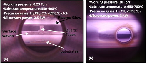
The seeded substrates were loaded into linear antenna microwave plasma-enhanced CVD reactor (LA MW PECVD). About 5% CH4 gas was flown into the chamber in the presence of high hydrogen gas concentration of 89%. About 6% CO2 gas was also added in the precursor gas mixture to promote etching of the non-diamond phases, leading to the growth of high-quality diamond films (). The base pressure was less than 10−4 Torr and the operating pressure was 0.23 Torr. Two sets of deposition were carried out: one set for 4 h and another set for 69 h of duration, respectively. The substrate temperature was around 400ºC during the diamond growth process. Two microwave sources, each with individual input power of 2500 W, and a distributed array of four antennas inside quartz tubes, were present in the reactor.
On the other hand, the resonant cavity reactor CVD deposition conditions were high temperature of 650º–700ºC and high pressure of 30 Torr, as shown in , with the use of 1% CH4 in 99% H2 (400 sccm of total gas flow rate) during two types of deposition periods 2 h (short) and 64 h (extended). Inside both the reactors, the CVD parameters, which are conducive for growing nanocrystalline diamond (NCD) films was adapted [Citation44], to investigate the effect of Si substrate roughness on the nucleation and growth behaviour of the NCD films.
2.3. Diamond film characterizations
Laser in-situ interferometer was used to measure the thickness of the growing film, which was further verified by the cross-sectional scanning electron microscopy (SEM – FEI Quanta 200 FEG). SEM also revealed the as-grown morphology of the diamond films. Raman spectra were recorded with a HORIBA Jobin Yvon T64000 spectrometer using laser light of 488 nm wavelength. AFM (Bruker Multimode 8 in tapping mode) was also used to observe the early diamond growth stages.
3. Results and discussion
3.1. Profilometer and contact angle measurements – effect of substrate roughness on hydrophilicity of substrates
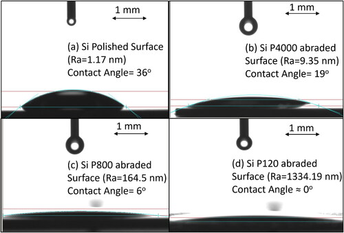
describes the surface roughness created on silicon surfaces and shows its effect on hydrophilicity over few such surfaces. The as-received p-type silicon wafer surfaces are one side polished with 1.17 nm average surface roughness (Ra, ) and the unpolished backside of the same wafer has a surface roughness of Ra = 305.59 nm. The contact angles measured on both the sides of the as-received wafer with distilled water, showed values of 36º and 28º, respectively, for the polished and the rough surfaces. The as-received wafer might have some organic contamination which did not cause significant difference in between the hydrophobic behaviour of the opposite faces of the same silicon wafer, although their roughness values were significantly different. The silicon surfaces were abraded with different grit sizes of emery paper and subsequently they were cleaned with acetone and alcohol to remove contamination during grinding. In addition, the surfaces were also cleaned with oxygen plasma for 10 min to remove any remnant organic contamination [Citation43]. Now, when such cleaned surfaces were tested for their hydrophilic nature (days after O2 plasma cleaning), they showed gradual decrease in contact angles. The substrate surfaces with very high roughness (P800, Ra = 164 nm onwards) were completely wetted with water (contact angles <6º or even less values which are beyond detection limit of the instrument). The finest grit size P4000 emery paper could produce a roughness of Ra = 9.35 nm on the mirror polished surface with initial Ra = 1.17 nm. On the other hand, the coarsest grit size emery paper P120, could make the smooth surface as highly rough as Ra = 1334.19 nm. Scratching the silicon wafers with different grades of emery papers made the surfaces rough and thereby made them hydrophilic [Citation13], conducive for subsequent seeding step with DND water suspension. Another method was adopted to create surface roughness, i.e. Ar ion treatment. Ion milling is routine procedure for preparing the electron microscopy test samples, however, in this work, it was adopted to create surface roughness. It was found that the mirror polished silicon surfaces became rough by argon ion milling with Ra = 11.29 nm, which is almost equivalent to scratching the surface with P4000 emery paper. It will be shown later, that although the values of roughness they produced are equivalent, but the subsequent effect on the nucleation and growth of CVD grown diamond on argon ion milled surfaces are significantly different than mechanically scratched surfaces. The relative difference between the manually scratched surface and the argon ion milled surface is reflected by the contact angle values. The silicon surface scratched with P4000 emery paper showed contact angle of 19º, whereas the surface treated with Ar+ ion plasma for 1 h was completely wet with water with 0º contact angle. Rabinovich et al. [Citation45] earlier showed that the nanoscale surface roughness (less than 20 nm) plays an important role in determining the adhesion force between the interacting particles and surfaces. The adhesion force starts decreasing for low surface roughness (≈ 1 nm); however, the same adhesion force increases again when the roughness becomes more than 10 nm. However, it is observed that although the P4000 abraded and the Ar+ ion milled Si surfaces had equivalent surface roughness, but their hydrophilicity was significantly different. This also may be due to their differences in surface characteristics, like compositions, chemical groups attached, etc. However, in the present set of experiments the only difference was the method in creating Si surface roughness. Mechanical abrasion was random scratching by “micron” size grits, whereas Ar+ ion milling was creation of surface ”nanostructures” by atom size plasma gas species. 100 min of argon plasma treatment cleaned the silicon surface thoroughly to produce complete hydrophilicity.
Figure 2. Profilometer scans of the substrates after surface treatments. The samples have been arranged in the increasing order of Ra surface roughness: (a) Si front face – 1.17 nm, (b) Si P4000 – 9.35 nm, (c) Si Ar+ milled – 11.29 nm, (d) Si P800 – 164.5 nm, (e) Si back face – 305.59 nm and, (f) Si P120 – Ra 1334.19 nm. (abscissa is the scan length of 5 mm and the ordinate is the average roughness expressed in nm. As every sample has different orders of roughness values, the grid line widths along the y-axis are different for all the samples. The red and green portions are, the initial and final lengths of stylus scans in mm, which were excluded during the average roughness calculations by the software.).
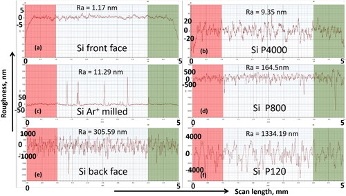
Figure 3. Effect of Si surface roughness creation by abrasion on their hydrophilicity – contact angles: (a) Si polished surface – 36º, (b) Si P4000 – 19º, (c) Si P800 – 6º and, (d) Si P120 ∼ 0º (equivalent length of the double headed arrow scale bar is 1 mm).
3.2. AFM and Raman – effect of substrate roughness on enhancing DND seeding density
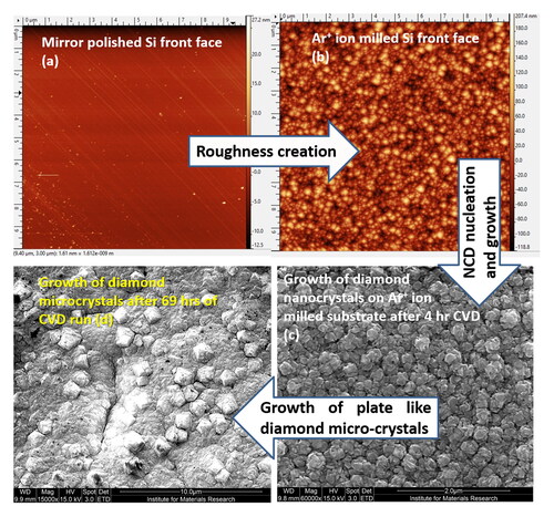
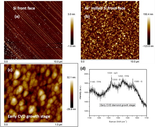
shows the different surface topographies of the as received mirror polished silicon surface and, the silicon surface treated with Ar+ ion plasma. The as-received silicon surface has inherent polishing marks on them. On the other hand, the argon ion milled surface in is uniformly damaged (2.6 × 10¹³/cm2 surface damage density). The profilometer scan of such argon treated surface shows intermittent spikes due to the formation of pits across the silicon surface ().
Figure 4. AFM scans of the (a) as-received silicon wafer surface, (b) argon ion milled silicon surface, (c) after 5-min resonant cavity CVD growth on the silicon surface shown in figure (a) with DND seeds, (d) Raman signals from the diamond crystals shown in figure (c).
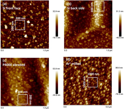
When such intentionally created rough surfaces were seeded with DND seeds in water suspension, then it was found to enhance the seeding densities, as shown in . The AFM scan of the DND-seeded mirror-polished silicon front surface shows a seeding density of 2 × 10¹⁰/cm2 in . But the back side of the same silicon wafer shows preferential alignment of the DND seeds along the grooves on the unpolished surface – thus enhancement of the seeding density (6 × 10¹⁰/cm2) as evident from . Similar enhancement of the seeding densities (5 × 10¹⁰/cm2) is observed in for the silicon surface treated with P4000 emery paper – it shows to densely populate the mechanically scratched grooves on the silicon surface. The AFM scan areas in are 1 µm × 1 µm, whereas shows an AFM scan of Ar+ ion milled silicon surface with agglomerated DND seeds (density of 1.2 × 109 cm−2) over 5 µm × 5 µm area. Surprisingly, there is five times increase (≈30 to ≈150 nm) in the individual DND seed sizes under the AFM scan for the Ar plasma treated silicon surface. Such distinction found in AFM images of the DND seeded surfaces, between the Ar+ ion milled and the mechanically scratched silicon surfaces, is also reflected in the respective SEM morphology images of the treated silicon surfaces, as discussed in the subsequent sections.
Figure 5. AFM images of DND seeded silicon substrates with seeding densities of (a) front face – 2 × 1010 cm−2, (b) back side – 6 × 1010 cm−2, (c) P4000 abraded – 5 × 1010 cm−2 and, (d) Ar+ milled – 1.2 × 109 cm−2.
The density of diamond grains (seeds grown bigger to touch each other) was also attempted to be calculated after 5 min of growth inside the resonant cavity CVD chamber on the DND seeded polished silicon surface, as shown in . The Raman signal from such diamond grains, just grown enough to fully cover the underneath Si surface, is shown in . It is observed that the diamond (sp3) Raman peak is present at 1332 cm–1, along with the peaks, corresponding to trans-polyacetylene (TPA) and disordered graphite (D) and crystalline graphite (G), with very low intensities.
It appears that after 5 min of diamond CVD growth, the DND seeds grow very fast in lateral direction to cover the silicon surface and started to touch each other – thereby forming grain boundaries. If and are compared, it is found that 30–50 nm size features have grown into more than 100 nm sizes to coalesce with each other. But surprisingly, such coalescing feature of the DND/diamond grains are already present in freshly seeded silicon surface when it was treated with the argon plasma (). Although such ion milling did not produce high surface roughness (11.29 nm), but it made the surface completely hydrophilic such that it was having 0º contact angle. Moreover, ion bombarded surface was having uniform pits and craters which also helped in effectively seeding the silicon surface.
3.3. Ar+ ion milling effect on diamond film morphologies – SEM
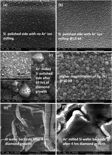
It has already been discussed in Section 3.1. that the roughness created by argon ion milling/etching on the silicon substrates helped in creating surfaces conducive for water based DND seed suspension with zero contact angles. It helped in uniformly covering the substrate surface with agglomerated DND particles. Such uniform seeding densities in contrast to non-uniform or scattered DND seeds on untreated/unscratched silicon surface () also observed to affect the morphological difference between the untreated and the Ar+ ion milled substrate surfaces, as shown in , after the CVD growth of diamond films. shows that the NCD grains are elongated, square shaped or in irregular shapes with approximately 95 nm average grain sizes, when grown for 4 h of duration inside the linear antenna CVD chamber at very low temperature of 400 °C [Citation46]. Whereas, during the same deposition conditions, the growth on the Ar+ ion milled silicon substrate kept alongside the untreated silicon surface, could produce much larger and uniform diamond film with granular morphologies (approximately 150 nm average grain sizes), as shown in . The magnification of is ¼th smaller than 6a, but the apparent grains sizes are almost similar. Therefore, it may be inferred that the Ar+ ion milled surfaces are promoting bigger and uniform grain morphologies when both are grown simultaneously by putting them side by side. It was important to further magnify such uniform NCD morphologies, as shown in . The apparent round shaped morphologies are consisting of tiny elongated or somewhat irregular shaped diamond grains. Essentially, the individual round morphology has many secondary nucleation sites, very typical of nanodiamond surface morphology grown by low temperature CVD [Citation46]. On the other hand, such NCD morphology transforms into micro-crystalline diamond (MCD) morphology with 1–2 µm average grain sizes () when the diamond film was allowed to grow over long hours (69 h) of LACVD run, under identical process recipes. The octahedral shapes (double headed dotted line in ) of the individual diamond grains become visible, although they are not as densely populated as the round shaped grains which was observed over the short duration CVD runs (a comparison between the inset of , at same magnification of 15K). The similar effect of Ar+ ion milling can also be found on the morphological difference between the diamond films grown on the unpolished back side of the silicon wafers. The profilometer scan data () and consequent contact angle measurements have already shown the effective nucleation enhancement due to roughness and preferential alignment of DND seeds along the grooves and pits of the unpolished back side of the silicon substrate wafer (). Now such effect is also observed in the as-grown NCD morphological difference between the argon treated and the untreated wafer backside. shows a smaller diamond nanocrystal size than in , which are the diamond nanocrystals grown on the Ar+ ion milled silicon wafer backside under the identical CVD growth conditions inside the linear antenna reactor. Therefore, it is inferred that additional treatment of substrate surface with argon ions, in both the cases of silicon wafer, the polished front side and the unpolished backside, makes bigger NCD crystals during CVD growth processing. The most positive impact of the Ar+ milling is to make a uniform distribution of the shapes and the sizes of the diamond grains. Such uniform nature of grain size distribution may have a positive impact in making uniform diamond surface properties. The reason behind producing uniform shape and sizes of the NCD grains with argon ion milling is that the “surface damages” created by Ar+ plasma was more “uniform” than the “surface damages” created by the solid particles embedded in the emery papers. The scale of “roughness uniformity”, in case of mechanical grinding was much less than the scale of “roughness uniformity” created by the argon ions. It is well reflected in , where the profilometer scan by 2 µm stylus on the Ar+ ion milled surface, produced much less “scattering of data” in the average roughness profile Ra values, than the roughness profile scans of the mechanically scratched silicon substrate surfaces in . The line profile in is almost as smooth as the line profile in for the as received polished silicon surface. The only apparent difference in between is the intermittent appearance of 1 Å wide (a gross approximation) and 100–150 nm deep pits on the line scan of the argon treated silicon surface. In other words, the Ar+ milling created uniform surface damages conducive for uniform CVD diamond nucleation and growth, but simultaneously, did not alter the average surface roughness of the silicon surface – which is beneficial for many practical applications [Citation38, Citation39].
Figure 6. SEM images of CVD grown NCD on (a) mirror polished silicon surface at magnification 60KX irregular shaped grains (4 h growth); (b) regular round shape morphology NCD after 4 h growth at magnification 15KX on Ar+ ion milled substrates, (c) MCD morphology after 69 h of growth at magnification 60KX and inset figure shows 15KX magnification image, on Ar+ ion milled substrates, (d) uniform rounded NCD grains at 60KX magnification from figure (b); (e) NCD on untreated silicon wafer unpolished backside and; (f) NCD on Ar+ ion milled silicon wafer unpolished backside.
3.4. Effect of deposition time on diamond film morphology and quality – SEM and Raman spectra
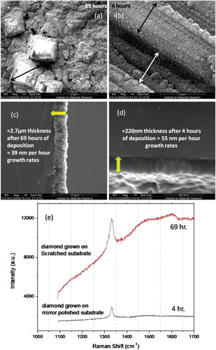
It has already been seen that the diamond film morphology changes from nanocrystalline to microcrystalline when it is allowed to grow for longer duration inside the linear antenna microwave plasma CVD system for the Ar+ ion milled silicon substrate surface (Section 3.3). This is also found to be true for the mechanically scratched substrates (“PX”). shows the morphology after 69 h of CVD growth and shows the diamond film grown under similar conditions but for shorter duration CVD growth of 4 h, inside linear antenna CVD chamber. The substrate surface for both the figures is the silicon scratched with P800 emery paper. It is observed in that the grooves created by scratching are of almost 2 µm in width, which were still visible after 4 h of CVD diamond deposition. The advantage of the linear antenna CVD diamond growth is that it produces conformal NCD coatings which follow the contours of the underlying substrate. Such templating of substrate contours is helpful for coating 3D structures as reported earlier [Citation27]. With increasing time, the films grow in columnar fashion and produces laterally flat surface morphologies as shown in . The diagonals of such flat grains are 1–2 µm in length. The cross-sectional diamond film microstructures are shown in . They show the columnar nature of the CVD grown diamond films. The film growth rates were initially faster at 55 nm/h and later with increasing time, it became sluggish to grow along the z-direction with a growth rate as slow as 39 nm/h, observed over a 3 d-long CVD experimental run. Now, this is since the diamond film starts to grow laterally (rather not vertically), and the film morphology changes from nanocrystalline to microcrystalline flat plate like morphology, during the long duration CVD runs (as also reported earlier [Citation46]). In other words, the linear antenna CVD diamond growth promotes flat grain morphology or growth in lateral direction than in the perpendicular direction. shows a flat grain (1–2 µm) on the film surface which is almost equivalent to the thickness (2–3 µm) of the film, as shown in along the z direction. The Raman signals from such diamond surfaces [Citation47], grown over different duration of time, are also found to be different, as shown in . The intensity of the sp3 peak at 1332 cm−1 is much higher for the diamond film grown over 3 d (on manually scratched substrate) than the sp3 signal from the film grown (on the as-received silicon substrate) over 4 h of CVD run. The diamond peak position for the microcrystalline grains is somewhat both up and down shifted with peak splitting, which is typical for films with biaxial stress. The diamond films are indeed grown anisotropically, i.e. “flat plates” in the lateral direction and “columnar” structures in the perpendicular direction, as evident from the previous SEM images. The bumps around 1450 and 1580 cm−1 positions in for the diamond grown on the scratched surface are due to the TPA and crystalline graphitic (G) inclusion in the films. TPA peaks also typically found at 1140 cm−1 for the NCD films grown inside linear antenna system. Such non-diamond peaks are unexpectedly not prevalent in the Raman spectra ( bottom signal) from the diamond film grown over mirror polished silicon surface during the shorter period of 4 h of CVD growth. It is because the films are grown purer on the unscratched substrates than the films grown on mechanically scratched wafers. Moreover, the films grown over 69-h CVD run period, also showed background luminescence, as the spectra moves upwards with increasing Raman shift. This can be due to the presence of defect centres in the laterally grown flat film morphologies.
Figure 7. SEM images of the (a) MCD after 69 h CVD growth, (b) NCD after 4 h CVD growth, at 60KX magnification for silicon substrates scratched with P800 emery paper; cross-sectional images for columnar structures- (c) after 69 h CVD growth, (d) after 4 h CVD growth (e) Raman spectra for diamond films grown on scratched and unscratched wafers at different time intervals.
3.5. Effect of reactor types on morphology and quality of diamond films – SEM and Raman spectra
The results from the nucleation and growth experiments of the diamond films deposited on rough substrates but grown inside two different classes of CVD reactors – at different pressure and temperature growth regimes will be presented and discussed in this section. The respective CVD processing conditions (recipes conducive to promote NCD film growth) have already been depicted in and Section 2.2.
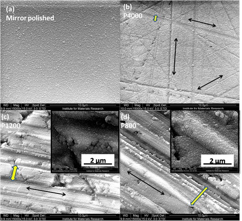
is the microstructures of the NCD films grown inside linear antenna reactor for 4 h on silicon surfaces with different roughness, as produced by scratching with different grades of emery papers, already shown in . All the surfaces are uniformly coated without any pinholes, which is the evidence of effective nucleation and CVD growth process. is the NCD on the polished silicon surface without any surface irregularities, whereas the diamond film on the silicon surface scratched with the finest P4000 grade emery paper shows scratching marks in random directions, shown inside by black double headed arrow lines. The widths of such scratched lines are very small (sub-micron, 0.3–0.6 µm) in , shown by yellow double headed solid arrows. Such scratching mark widths are found to be increasing with the increasing grit sizes of the emery papers, from P4000, to P1200 and up to P800. The magnifications of all the images in are same, i.e. 15KX, however, with the increasing grit sizes of the abrasives used for scratching, the widths of the scratching marks become wider, and it appears to become the predominant morphological feature of the grown films (). The dimensions of the substrate scratching marks are in microns range, whereas the CVD grown NCD grains present inside the scratched groves are much smaller in–size - which thereby helps in conformal covering of the entire substrate surface. The insets of presented the higher magnification images to show the NCD films more clearly, which are having average grain sizes from 80 to 100 nm.
Figure 8. SEM morphologies of the NCD films on substrates (a) mirror polished silicon – 1.2 nm, (b) P4000 – 9.3 nm, (c) P1200 – 92.4 nm, (d) P800 – 164.5 nm, with different surface roughness (Ra) at identical magnification of 15KX, inside linear antenna microwave plasma enhanced CVD system. The inset images in (c) and (d) were taken at higher magnification of 60KX.
The diamond films grown under conventional resonant cavity CVD reactor at higher pressure and higher temperature conditions are shown in . Such reactor is found also to produce NCD grains without any pinholes, confirming effective nucleation pre-treatment by mechanical scratching and subsequent CVD growth.
Figure 9. SEM morphologies of the NCD on scratched substrates (a) P1200 – 92.4 nm, (b) P800 – 164.5 nm, (c) P320 – 500 nm, (d) P180 – 825 nm, with different surface roughness (Ra) at identical magnification of 50KX, grown inside resonant cavity microwave plasma enhanced CVD system for 2 hrs. The inset images were taken at higher magnifications of 100KX.
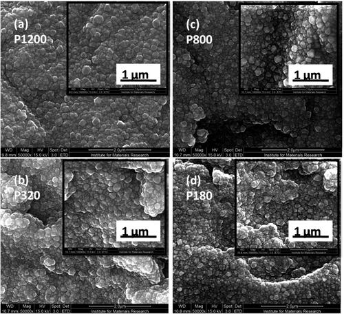
The deposition inside resonant cavity reactor produces similar nanocrystalline grains although within shorter time of only 2 h of CVD deposition. The substrate temperature was at 650º – 700ºC, which led to faster growth of NCD grains than inside the linear antenna CVD chamber. Moreover, the pressure regimes are also completely different between these two types of CVD reactors. The linear antenna low pressure CVD produced flat film morphology promoting preferential growth in the lateral dimension, whereas the resonant cavity CVD does not promote such preferential growth in the lateral direction with reference to the base substrate. shows that the diamond films are having average grain sizes from 80 to 100 nm, when they were grown on mechanically scratched silicon substrates inside the resonant cavity system. There is not much difference observed in between the respective NCD grain sizes, when the diamond films were grown over different substrates with different roughness. Also, there is not much surface morphological difference between the diamond films grown under two different CVD deposition processing conditions. The only significant difference observed was, the flat plate like microcrystalline diamond (MCD) morphologies that were present inside NCD matrix, for the long duration (69 h) run inside the linear antenna CVD reactor (). However, it will be seen later that resonant cavity also could produce flat plate like diamond microcrystals during the long periods of CVD growth.
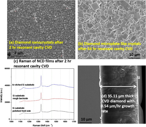
is the SEM morphology of the diamond nanocrystals deposited on mechanically scratched Si surface (abraded by P4000 emery paper) after 2 h growth inside the resonant cavity CVD chamber. Whereas such 147–178 nm size diamond nanocrystals deposited during 2 h CVD run, were found to grow into 1–6 μm size micron plates () after 64 h of CVD growth inside the resonant cavity reactor. In (b), it is observed that (100) or (110) square plate like crystal orientations were deposited in this study, inside the resonant cavity CVD growth conditions (with 1% CH4 in H2 at 400 sccm total gas flow rate). Such deposition parameters for resonant cavity CVD growth were preferred, as it was found earlier in that the diamond film grown for shorter duration CVD growth of 4 h, inside linear antenna CVD chamber, changes to flat plate like MCD morphology in after 69 h of CVD growth (also refer to ). The thickness of diamond coating deposited over 64 h was about 35 μm () and the growth rate was calculated to be 0.54 μm/h inside such resonant cavity CVD chamber. Raman spectroscopy signals, from the diamond films grown simultaneously on variety of substrates, inside resonant cavity CVD chambers, show almost identical spectra in . All of the films, deposited onto differently treated silicon surfaces, had peaks at 1332 cm−1, 1580 cm−1 and at 1140 cm−1 and 1450 cm−1 which correspond to sp3, sp2, and TPA carbons, respectively [Citation46]. The quality of the diamond film is reported as the relative integrated area peak intensities of the sp3 carbon peak at 1332 cm-1 to other non-diamond carbon peaks. shows that the diamond sp3 bonded peaks are more intense for the films on the mirror polished side and for the films on the Ar+ ion milled/etched silicon surface. Whereas the sp3 peak intensity for the film grown on the unpolished silicon backside wafer is somewhat suppressed. This may be because the roughness helped in producing better quality films with less non-diamond carbon phase formation. But it was not the case for the quality of the diamond films grown on the Ar+ ion milled silicon surface.
Figure 10. (a) SEM image of the diamond nanocrystals grown over P4000 abraded Si substrate after 2 h growth, (b) SEM image of the diamond micro-plates grown over mirror polished Si after 64 h growth, (c) Raman spectra of the different NCD films on substrates with different surface roughness after 2 h CVD growth, (d) cross-sectional SEM of the diamond coating shown in – all were grown inside resonant cavity microwave plasma enhanced CVD system.
The CVD growth processes appeared to be different in between the low temperature linear antenna CVD reactor and the conventional resonant cavity high temperature deposition CVD chamber. The pressure inside both types of reactors and the plasma volume densities are completely different [Citation44]. Therefore, to estimate the relative NCD film qualities grown by the two different reactors, the Raman spectra of and are compared. It is observed that in both the cases, NCD films grown over Si mirror polished side is of better quality than the films grown over mechanically scratched Si surfaces. In order to quantify the different diamond film qualities grown over the rough substrate surfaces, the integrated area over the diamond peak position at 1332 cm−1 (Isp3) and the integrated area over the non-diamond bands from 1400 to 1744 cm−1 (Inon-sp3) were calculated [Citation48]. Then a relative Raman peak area ratio of the diamond to non-diamond carbons, in percentages, provide an indication of the grown diamond film quality, i.e. Q = Isp3 / (Isp3 + Inon-sp3). It was found that the films grown inside resonant cavity reactor onto mirror polished silicon surface is 43.24% good in diamond quality, like the quality of the diamond grown on Ar+ ion milled silicon surfaces, which is 42.78%. But the diamond film quality is considerably poorer 33.47% for the NCD deposited on mechanically scratched Si substrates. The Raman spectra in , from the films grown inside linear antenna system showed somewhat better quality 44.95% for the NCD deposited on mirror polished surface. However, the quality of the films deposited on the Ar+ ion milled Si surface could not be calculated by integrating the area of the diamond to the non-diamond peaks due to the inherent fluorescent nature of the Raman spectrum.
The key experimental results and discussion are summarised in to enhance reader comprehension and facilitate a more comprehensive understanding of the experimental data.
Table 1. Summary of the important experimental results.
4. Conclusions
The important conclusions are as follows:
Silicon surfaces were mechanically scratched to produce different surface roughness, which could effectively enhance the hydrophilicity of the substrates.
Ar+ ion milling could uniformly scratch/damage (2.6 × 1013cm−2) the silicon surface and successfully did not produce very high surface roughness (Ra ≈11 nm).
Roughness enables preferential alignment of DND seeds along the grooves and pits on the silicon surfaces.
DND seeds were more densely populated on the rough Si surfaces (6 × 1010 cm−2) than on the unscratched flat Si substrate (2 × 1010 cm−2).
DND seeding efficiency, in terms of its density (1.2 × 109 cm−2) and seed sizes (150 nm) were greatly enhanced for the Ar+ ion milled surfaces. Such specially treated surfaces are completely hydrophilic (0º contact angle) which further facilitates coverage of the water based DND suspension on silicon substrates.
Ar+ ion milled Si surfaces produced uniformly dispersed spherical NCD grains (unique feature) after subsequent CVD growth.
There was not much difference in the NCD grain sizes (80–180 nm) between the films grown under two different CVD reactor systems, namely linear antenna and resonant cavity, both using 2.45 GHz frequency at almost similar power levels (≈3 kW) for shorter CVD runs (2–4 h) on rough Si substrates.
The NCD films were following the rough substrate surface template without any pinhole formation at the top surface, which is important in view of potential application for coating 3D structures. The NCD grains became 1–6 μm average size MCD crystals if they were allowed to grow over long periods (64–69 h). Both the rector types produced flat plate like MCD morphologies, after long hours of CVD runs.
Authors’ contributions
AKM: conceptualization, methodology, formal analysis, investigation, resources, data curation, writing – original draft preparation, writing – review and editing, visualization; RR: conceptualization, methodology, formal analysis, investigation, resources, data curation, writing – review and editing, visualization; FL: conceptualization, methodology, formal analysis, investigation, resources, data curation, writing – review and editing, visualization; RMJ: methodology, formal analysis, investigation, resources, writing – review and editing; KH: conceptualization, validation, writing – review and editing, visualization, supervision, project administration, funding acquisition.
| Abbreviations | ||
| AFM | = | Atomic force microscopy |
| CVD | = | Chemical vapor deposition |
| D | = | Disordered graphite |
| DND | = | Detonation nanodiamond |
| G | = | Crystalline graphite |
| I | = | Intensity |
| KX | = | Electron microscope image magnification |
| Ra | = | Surface roughness in nm |
| LA MW P ECVD | = | Linear antenna microwave plasma enhanced |
| CVD | = | reactor |
| LACVD | = | Linear antenna CVD |
| MCD | = | Micro-crystalline diamond |
| NCD | = | Nanocrystalline diamond |
| P X | = | Abraded sample identification number, treated with different grades (X) of emery paper (P) |
| Q | = | Quality |
| TPA | = | Trans-polyacetylene |
Acknowledgments
We thank our colleague Prof. Jan D’Haen for taking the SEM data and Dr. P. Pobedinskas for the Raman spectroscopy data. All data generated or analysed during this study are included in this published article. The datasets generated during and/or analysed during the current study are available from the corresponding author upon reasonable request.
Disclosure statement
The authors declare that they have no known competing financial interests or personal relationships that could have appeared to influence the work reported in this article.
Additional information
Funding
References
- Gunn DJ. Effect of surface roughness on the nucleation and growth of calcium sulphate on metal surfaces. J Cryst Growth. 1980;50(2):533–537.
- Campbell JM, Meldrum FC, Christenson HK. Is ice nucleation from supercooled water insensitive to surface roughness? J Phys Chem C. 2015;119(2):1164–1169.
- Wind RW, Fabreguette FH, Sechrist ZA, et al. Nucleation period, surface roughness, and oscillations in mass gain per cycle during W atomic layer deposition on Al2O3. J Appl Phys. 2009;105(7):074309.
- Chan CY, Eyhusen S, Meng XM, et al. The effect of substrate surface roughness on the nucleation of cubic boron nitride films. Diamond Relat Mater. 2006;15(1):55–60.
- Ying Z, et al. Effect of substrate micro-morphology on heterogeneous nucleation. China Found. 2012;9:234–238.
- Tien LC, Chen YJ. Effect of surface roughness on nucleation and growth of vanadium pentoxide nanowires. Appl Surf Sci. 2012;258(8):3584–3588.
- Holbrough JL, Campbell JM, Meldrum FC, et al. Topographical control of crystal nucleation. Crystal Growth Design. 2012;12(2):750–755.
- Liu YX, Wang XJ, Lu J, et al. Influence of the roughness, topography, and physicochemical properties of chemically modified surfaces on the heterogeneous nucleation of protein crystals. J Phys Chem B. 2007;111(50):13971–13978.
- Zhang Y, Wang M, Lin X, et al. Effect of substrate surface microstructure on heterogeneous nucleation behavior. J Mater Sci Technol. 2012;28(1):67–72.
- Mu C, Pang J, Lu Q, et al. Effects of surface topography of material on nucleation site density of dropwise condensation. Chem Eng Sci. 2008;63(4):874–880.
- Qi Y, Klausner JF, Mei R. Role of surface structure in heterogeneous nucleation. Int J Heat Mass Transf. 2004;47(14–16):3097–3107.
- Ohring M. Materials science of thin films. 2nd ed. Cambridge (MA): Academic Press; 2002.
- Zeng Q, Xu S. Thermodynamics and characteristics of heterogeneous nucleation on fractal surfaces. J Phys Chem C. 2015;119(49):27426–27433.
- Page AJ, Sear RP. Crystallization controlled by the geometry of a surface. J Am Chem Soc. 2009;131(48):17550–17551.
- Mandal S. Nucleation of diamond films on heterogeneous substrates: a review. RSC Adv. 2021;11(17):10159–10182.
- Higuchi K, Noda S. Selected area diamond deposition by control of the nucleation sites. Diamond Relat Mater. 1992;1(2–4):220–229.
- Ascarelli P, Fontana S. Dissimilar grit-size dependence of the diamond nucleation density on substrate surface pretreatments. Appl Surf Sci. 1993;64(4):307–311.
- Buijnsters JG, Vázquez L, ter Meulen JJ. Substrate Pre-Treatment by ultrasonication with diamond powder mixtures for nucleation enhancement in diamond film growth. Diamond Relat Mater. 2009;18(10):1239–1246.
- Lee ST, Lin Z, Jiang X. CVD diamond films: nucleation and growth. Mater Sci Eng R. 1999;25(4):123–154.
- Pobedinskas P, Janssens SD, Hernando J, et al. Selective seeding and growth of nanocrystalline CVD diamond on non-diamond substrates. MRS Proc. 2011;1339:1339.
- Rotter SZ, Madaleno JC. Diamond CVD by a combined plasma pretreatment and seeding procedure. Chem Vap Deposition. 2009;15(7–9):209–216.
- Arnault JC, Demuynck L, Speisser C, et al. Mechanisms of CVD diamond nucleation and growth on mechanically scratched Si (100) surfaces. Eur Phys J B. 1999;11(2):327–343.
- Shenderova O, Hens S, McGuire G. Seeding slurries based on detonation nanodiamond in DMSO. Diamond Relat Mater. 2010;19(2–3):260–267.
- Williams OA, Douhéret O, Daenen M, et al. Enhanced diamond nucleation on monodispersed nanocrystalline diamond. Chem Phys Lett. 2007;445(4–6):255–258.
- Haenen K, Pobedinskas P, Ramaneti R. Growing diamond layers. Patent no. EP3745446A1. 2020 Feb 12.
- Anger E, Gicquel A, Wang ZZ, et al. Chemical and morphological modifications of silicon wafers treated by ultrasonic impacts of powders: consequences on diamond nucleation. Diamond Relat Mater. 1995;4(5–6):759–764.
- Domonkos M, Ižák T, Varga M, et al. Diamond nucleation and growth on horizontally and vertically aligned Si substrates at low pressure in a linear antenna microwave plasma system. Diamond Relat Mater. 2018;82:41–49.
- Stoner BR, Ma GHM, Wolter SD, et al. Characterization of bias-enhanced nucleation of diamond on silicon by invacuo surface analysis and transmission electron microscopy. Phys Rev B. 1992;45(19):11067–11084.
- Maillard-Schaller E, Küttel OM, Gröning P, et al. Local heteroepitaxy of diamond on silicon (100): a study of the interface structure. Phys Rev B. 1997;55(23):15895–15904.
- Pobedinskas P, Degutis G, Dexters W, et al. Surface plasma pretreatment for enhanced diamond nucleation on AlN. Appl Phys Lett. 2013;102(20):201609.
- Damm DD, Contin A, Cardoso LDR, et al. A novel method to mitigate residual stress in CVD diamond film on steel substrates with a single intermediate layer. Surf Coat Technol. 2019;357:93–102.
- Mallik AK, Bysakh S, Bhar R, et al. Effect of seed size, suspension recycling and substrate pre-treatment on the CVD growth of diamond coatings. OJAppS. 2015;05(12):747–763.
- Mallik AK, Mendes JC, Rotter SZ, et al. Detonation nanodiamond seeding technique for nucleation enhancement of CVD diamond – some experimental insights. Adv Ceramic Sci Eng. 2014;3(0):36–45.
- Mallik AK, Binu SR, Satapathy LN, et al. Effect of substrate roughness on growth of diamond by hot filament CVD. Bull Mater Sci. 2010;33(3):251–255.
- Mandal S, Thomas ELH, Middleton C, et al. Surface zeta potential and diamond seeding on gallium nitride films. ACS Omega. 2017;2(10):7275–7280.
- Bland HA, Thomas ELH, Klemencic GM, et al. Superconducting diamond on silicon nitride for device applications. Sci Rep. 2019;9(1):2911.
- Li X, Gao Y, Ge P, et al. Nucleation location and propagation direction of radial and median cracks for brittle material in scratching. Ceram Int. 2019;45(6):7524–7536.
- Possan AL, Menti C, Beltrami M, et al. Effect of surface roughness on performance of magnetoelastic biosensors for the detection of Escherichia coli. Mater Sci Eng, C. 2016;58:541–547.
- Perry SC, Gateman SM, Sifakis J, et al. Enhancement of the enzymetic biosensor response through targeted electrode surface roughness. J Electrochem Soc. 2018;165(12):G3074–G3079.
- Babchenko O, Potocký Š, Ižák T, et al. Influence of surface wave plasma deposition conditions on diamond growth regime. Surf Coat Technol. 2015;271:74–79.
- Kromka A, Potocký Š, Čermák J, et al. Early stage of diamond growth at low temperature. Diamond Relat Mater. 2008;17(7–10):1252–1255.
- Das D, Singh RN. A review of nucleation, growth and low temperature synthesis of diamond thin films. Int Mater Rev. 2007;52(1):29–64.
- Pobedinskas P, Degutis G, Dexters W, et al. Nanodiamond seeding on plasma-treated tantalum thin films and the role of surface contamination. Appl Surf Sci. 2021;538:148016.
- Drijkoningen S. Low temperature deposition and characterisation of high quality nanocrystalline diamond films for the fabrication of highly sensitive pressure sensing membranes. Belgium: Hasselt University; 2017.
- Rabinovich YI, Adler JJ, Ata A, et al. Adhesion between nanoscale rough surfaces. I. Role of asperity geometry. J Colloid Interface Sci. 2000;232(1):10–16.
- Drijkoningen S, Pobedinskas P, Korneychuk S, et al. On the origin of diamond plates deposited at low temperature. Crystal Growth Design. 2017;17(8):4306–4314.
- Mallik AK, Bysakh S, Sreemany M, et al. Property mapping of polycrystalline diamond coatings over large area. J Adv Ceram. 2014;3(1):56–70.
- Pal KS, Mallik AK, Dandapat N, et al. Microscopic properties of MPCVD diamond coatings studied by micro-Raman and micro-photoluminescence spectroscopy. Bull Mater Sci. 2015;38(2):537–549.