
 ?Mathematical formulae have been encoded as MathML and are displayed in this HTML version using MathJax in order to improve their display. Uncheck the box to turn MathJax off. This feature requires Javascript. Click on a formula to zoom.
Abstract
Experimental results showed that for the diamond film prepared by hot filament chemical vapor deposition (HFCVD) using Ta filament, TaC existed between diamond and the silicon substrate, and diamond grew directly on TaC, while the inherent mechanism was not clear. Here, a special coherent interface Diamond(111)//TaC(111) is observed using high resolution transmission electron microscopy, and then we explore the effects of the TaC with different lattice planes on the diamond formation by first-principle calculations. The results show that C tends to adsorb on the TaC(111) C-terminated surface. The strong covalent bond between C from diamond and Ta from TaC is formed in the Diamond(111)//TaC(111) interface, while only C–C covalent bonds are formed at the Graphite(002)/TaC(111). This makes diamond thermodynamically more stable than graphite on the TaC surfaces. Our investigations provide critical information to understand the complex diamond formation mechanism, especially with the presence of TaC.
1. Introduction
Hot filament chemical vapor deposition (HFCVD) is a widely used method for the preparation of diamond film at low-pressure, since it has the advantage of a fast growth rate and large deposition area [Citation1–4]. Eversole et al. successfully deposited diamonds at low pressure using the CVD method, and then Matsumoto et al. had been able to increase the growth rate of diamond by using hot metal filaments [Citation5]. The growth of diamond by HFCVD is influenced by many factors because of the complexity of the experimental condition. Song et al. [Citation6] found that when methane was used as the carbon source for diamond deposition, excessively high concentrations of methane increased the non-diamond phase, which reduced the growth rate of diamond. Yue et al. [Citation7] indicated that the temperature of the filament affected the reaction at its surface and thus governed the diamond film deposition.
Non-diamond phases are produced and affect the formation of diamond during the complex HFCVD deposition process. Various carbon allotropes, such as i-carbon [Citation8] and n-diamond [Citation9], provided new perspectives on the growth mechanism of nanodiamond vapor phase synthesis and HFCVD diamond. Park et al. [Citation10] observed that i-carbon and n-diamond were formed during the initial stages of diamond growth. Zhu et al. [Citation11] found that i-carbon occurred as a phase transition intermediate during the transformation of graphite to diamond at ordinary pressure. Furthermore, due to the use of hot metal filaments, the metal carbides phase inevitably be formed, which affects the nucleation and growth of diamond. Zhang et al. [Citation12] found that the WC interlayer acted as a diffusion barrier for carbon, thus significantly enhancing the nucleation properties of diamond. Aoki et al. [Citation13] reported that the WC transition layer provided nucleation sites for diamond growth, and the diamond(111) surface grew epitaxially on the WC(001) surface.
In addition to tungsten (W), tantalum (Ta) wire served as another prevalent metal filament [Citation7,Citation11,Citation14,Citation15]. Various methods involved the incorporation of Ta into diamond films during deposition. The introduction of monodisperse Ta atoms effectively reduced the potential barrier necessary for the phase transition, facilitating the ordinary-pressure transformation of graphite into diamond [Citation15]. Moreover, the formation of tantalum carbide (TaC) was an inevitable outcome during the growth of diamond films in HFCVD systems utilizing Ta filaments [Citation14,Citation16,Citation17]. TaC was assumed as a crucial role in the nucleation of diamond. Soto et al. [Citation18] undertook the preparation of TaC through HFPVD, transitioning from PVD to CVD. This strategic shift enabled the successful growth of diamond on in-situ deposited TaC. Interestingly, a composite of TaC and diamond powders exhibited a greater promotion of CVD diamond nucleation compared to using pure diamond powders [Citation19]. Nevertheless, the precise mechanism underlying diamond formation on TaC remains unclear.
In this work, we used Ta wire as the metal filament to grow nanodiamond film on the single-crystal silicon substrate in the HFCVD system. TaC was found to exist between silicon and diamond, and the diamond was grown directly on TaC, satisfying a special interface relationship: Diamond(111)//TaC(111). And then we investigated the structural stability and bonding properties of the interface by first-principles calculation. The results show that diamond is more stable than graphite on the TaC surface. Our results provide critical information to understand the complex diamond film formation, especially with the presence of TaC.
2. Experimental and calculation methods
2.1 Experimental method
2.1.1 Pretreatment of substrate
The nanodiamond films were deposited using the HFCVD method with single-crystal silicon, orienting along [100] axis, as the substrate (size of 10 × 10 mm2). Before deposition, the nanodiamond powder was mixed with deionized water in a ratio of 1:100 and sonicated in an ultrasonic machine for 5 min to obtain the abrasive solution. The silicon wafer was placed on a polishing cloth and polished with an abrasive solution for 30 min and sonicated in the abrasive solution for 30 min, then rinsed with deionized water and sonicated in an acetone solution for 5 min.
2.1.2 Preparation of nanodiamond films
Ta wires were used as the hot filaments and carbonized before the deposition of the nanodiamond films. (filament number = 6, diameter = 0.8 mm). The 8 pre-treated samples were placed 7 mm below the Ta filaments. During the diamond deposition, acetone as a carbon source, H2 gas was bubbling through acetone (∼80 sccm, maintained at 0°C), and extra amount of H2 gas (∼200 sccm) was introduced into the reaction chamber. The pressure of the chamber was maintained at 1 kPa. The growth power was set as 4400 W and the deposition time was 1 h. The temperatures of the Ta filament and the substrate were about 2200°C and 650°C, respectively.
2.2 Calculation method
In this work, the Vienna Ab initio Simulation Package (VASP) software package based on density functional theory (DFT) was adopted for all calculations [Citation20]. The Perdew–Burke–Emzerh (PBE) functional under the generalized gradient approximation (GGA) was used to describe the exchange-correlation energy [Citation21] and projector augmented wave potential (PAW) [Citation22] was used to deal with the interaction between ion and valence electrons. The Brillouin region was sampled by k-point grid of Monkhorst-pack method [Citation23]. In the calculations, the cut-off energy for bulk TaC and diamond was all set at 500 eV. The k-point sampling grids for bulk TaC and diamond were all set to 8 × 8 × 8, while that for the surfaces and interfaces were set to 7 × 7 × 1. The SCF convergence tolerance of the total energy was 10−6 eV/atom, and the maximum force was 0.001 eVÅ−1.
3. Result and discussion
3.1 Interfacial selectivity of diamond growth on TaC
We prepared diamond films in HFCVD system using Ta filaments. There is an obvious peak of 1332 cm−1 in the Raman spectrum (see ), corresponding to diamond. SEM (see ) also shows the typical morphology of nanodiamond films. To investigate the growth of diamond on the Si substrate, the sample was cut in cross-section using the focused ion beam (FIB) method and then characterized for the microstructure of the interface region between the diamond and Si substrate As shown in , there is a transition region between the diamond and Si substrate with the thickness of about 10 nm. The elemental distribution shows that the region is rich in Ta and C elements. O atoms are uniformly dispersed in this interface region and the amount of O atoms is very little compared to other elemental atoms (see Figure S1). Further, the transition layer was characterized at a higher magnification, and the composition of the transition layer was studied in region 1 near the diamond and region 2 near the Si substrate, and the regions were subjected to Fourier transform (FT). The FT of region 1 () shows the presence of two pairs of bright diffraction point, corresponding to diamond (111) plane with a crystalline spacing of 0.206 nm and the TaC(111) plane with a crystalline spacing of 0.264 nm. The lattice stripes are marked in red and yellow respectively in region 1, which are parallel to each other. In region 2, in addition to diamond (111) and TaC(111), there is a diffraction point corresponding to the Si(311) with a crystalline spacing of 0.131 nm (see ). The results show that during the growth of diamond on Si substrate, TaC forms on the Si surface firstly, and then diamond grows directly on the surface of TaC, forming a coherent interface and a special orientation relationship: Diamond(111)//TaC(111).
Figure 1. (a) Raman spectrum and (b) FESEM image of the as-deposited nanocrystalline diamond film; (c) low-magnification TEM image of the interface region; (I) the HAADF image; (II)-(IV) EDX mapping information of Si, Ta, and C, respectively. (d) High-magnification TEM image of the interface region, corresponding enlarged images and FT images of regions 1 and 2 in (b).
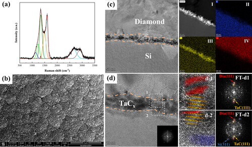
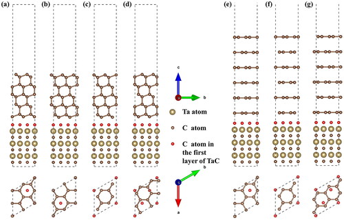
Figure 2. Side view and top view of the four different Diamond111)/TaC (111) interface models: (a) Dia-Model I, (b) Dia-Model II, (c) Dia-Model III, (d) Dia-Model IV, and the three different graphite (002)/TaC (111) interface models: (e) Gra-Model Ⅴ, (f) Gra-Model Ⅵ, (g) Gra-Model Ⅶ.
In Soto’s work [Citation18], TaC substrate provided excellent nucleation sites for diamond. Significantly, the XRD of the substrate showed a distinct peak corresponding to TaC(111). Li and coworkers [Citation16] clarified that TaC was formed during the deposition of the BDD films, and XRD profile of the diamond films deposited on the TaC exhibited the diffraction peaks characteristic of the Diamond(111) facet. The co-existence of two strong peaks, TaC(111) and Diamond(111), was observed by Mahtab [Citation17] in the XRD patterns of diamond films grown using Ta filaments. These are consistent with our conclusions. The special orientation growth relationship between TaC and diamond provides a clearer understanding of the complex formation process of diamond films deposited in HFCVD systems.
3.2 First-principles calculations of Diamond/TaC interfacial properties
To understand the formation mechanism of the interfacial structure, we studied the adsorption energy, structural stability and bonding properties of the interface by performing first-principles calculations.
3.2.1 Adsorption energy of C atom on the TaC surfaces
In order to clarify on which TaC surface C atom is more likely to adsorb during the deposition process, we calculated the adsorption energy of the C atom on three common TaC surfaces: TaC(111), TaC(110), and TaC(100). The convergence of these surfaces was carefully tested to determine the number of atomic layers required for the surface model to deliver accurate results with reasonable computation cost. It is noted that there are two types of termination for the TaC(111) surface: C-terminated and Ta-terminated. When the number of atomic layers (n) is odd, the plate model is symmetric, which can eliminate the dipole effect [Citation24]. So, the model with an odd atomic layer is applied in the following calculation. To determine the appropriate number of atomic layers, the change percentage () in the interlayer is calculated according to EquationEquation (1)
(1)
(1) as below:
(1)
(1)
where
represents the spacing between i and j layers in the unrelaxed crystal,
represents the spacing between i and j layers in the crystal after relaxation. The calculation results are shown in Table S1. Note that the increase of atomic layers, Δ12 and Δ23, reach converge gradually as the slab interiors exhibit bulk-like properties. The change in
of the first four layers of atoms is small when the number of atomic layers is increased to 7.
TaC(110) and TaC(100) are non-polar surfaces and surface energy equation is defined as EquationEquation (2)(2)
(2) :
(2)
(2)
where
is the surface energy of the TaC(110) or TaC(100),
is the total energy of the relaxed TaC(110) or TaC(100) surface model,
is the number of atoms of the TaC(110) or TaC(100) model,
is the number of atoms of the bulk TaC cell,
is the energy of the bulk TaC;, and
signifies the TaC(110) or TaC(100) surface area.
As shown in Figure S2, 6-layer TaC(110) and TaC(100) surface are convergent and used to calculate in this work. The results of adsorption energy are listed in . It is observed that the adsorption energy of the TaC(111) C-terminated surface is the smallest. So C atoms are more easily adsorbed on the TaC(111) C-terminated surface, which is consistent with our TEM results. Therefore, the 7-layer TaC(111) C-terminated surface is selected for the study of the interface.
Table 1. Adsorption energy of C atom on TaC surfaces.
3.2.2 Model construction and optimization
Based on our theoretical calculations and TEM results, we constructed the Diamond(111)/TaC(111) interface model. Considering that graphite is a competing phase for diamond during the deposition process [Citation25,Citation26], we constructed the Graphite(002)/TaC(111) interface model to compare the interfacial properties. The surface energy of diamond (111) with different atomic layers is shown in Table S2, which reveals that 10-layer Diamond(111) surface model is similar to the bulk structure, which is consistent with the calculations of Yue et al. [Citation27]. According to the calculation results of the above convergence test, the model of Diamond/TaC interface was built with a superlattice geometry, in which a 10-layer Diamond(111) slab and a 7-layer TaC(111) slab are combined with the orientation relationship: Diamond[1 0]ǁTaC[2
] and Diamond(111)//TaC(111). Based on the Bramfitt lattice mismatch theory [Citation28] that the lattice mismatch between two surfaces should be less than 6%, the lattice mismatches of Diamond(111)/TaC(111) are both about 4.42%, suggesting the formation of a coherent interface. Moreover, 6-layer graphite (002) slab and 7-layer TaC (111) slab are used to build the interface models, the lattice mismatches are about 5.4%. A 15 Å vacuum layer was added along the c direction in the model to avoid the interaction between the top and bottom layers.
There are four Diamond(111)/TaC(111) interface models and three Graphite (002)/TaC(111) interface models constructed, as shown in . The Dia-Model I, II, III, IV represent C atom in the first layer of TaC is located above the first layer of diamond, above the carbon atoms of the second diamond layer, above the carbon atom of diamond in the third layer, and between the two nearest carbon atoms in the first layer of the diamond, respectively. The Gra-Model Ⅴ, Ⅵ, and Ⅶ represents the C atom is located above the first layer of the graphite carbon atom, above the carbon atoms of the second graphite layer, and between the two nearest carbon atoms in the first layer of the graphite, respectively.
To construct the stable interfacial structure, we calculated the ideal adhesion work (Wad), which is defined as the reversible work required to separate the interface into two free surfaces. The greater the value of adhesion work, the more stable the interface structure. The Wad of these interfaces was calculated using a two-step approach. Firstly, according to the Universal Binding Energy Method (UBER) [Citation29], the total energy of the unrelaxed interface with different interface distances was calculated and the relationship between Wad and the different interface distances is shown in . The highest point of the curve corresponds to the maximum Wad and its optimal interface distance is listed in the “Unrelaxed (UBER)” column of . Secondly, the interfaces with the above optimal interface distance are fully relaxed and their Wad are listed in the “Fully relaxed” column of . The Wad is calculated by the following formula [Citation30]:
(3)
(3)
where
and
represents the total energy of diamond or graphite and TaC surface after fully relaxation, respectively,
denotes the total energy of the diamond or graphite/TaC interface, and
represents the interface area. Generally, when the adhesion work is larger, the bonding strength of the interface should be stronger and more stable.
Figure 3. Universal binding energy relation curves of four Diamond(111)/TaC (111) interfaces and three graphite (002)/TaC (111) interfaces.
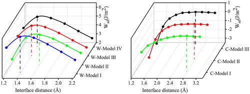
Table 2. Interface distance (d0), adhesion work (Wad) calculated using the two different methods (UBER and fully relaxation).
Among the four models for Diamond/TaC interface, Dia-Model I and Dia-Model IV, Dia-Model II and Dia-Model III have similar Wad, respectively. To explain the changes in Wad, we examined these atomic structures after relaxation (see Figure S3) and it was found that Dia-Model I and Dia-Model IV, Dia-Model II and Dia-Model III are similar, respectively, which is consistent with the result of the Wad. Among the three models of Graphite/TaC interface, Gra-Model Ⅴ and Gra-Model Ⅵ have similar Wad, and it is worth noting that the interface distance has been reduced significantly after the relaxation. In Figure S3, it is observed that a fraction of the C atoms in the first graphite layer in Gra-Model Ⅴ after relaxation have moved downwards to form elongated sigma bonds with the C atoms on the TaC surface, with the bond length of 1.61 Å. Gra-Model Ⅶ has the largest interface distance and the smallest value of Wad. The C atoms do not move and form bond with atoms in the TaC since the interface only relies on van der Waals force interactions and Coulomb forces paly an insignificant role. Moreover, Wad of Diamond/TaC interface (6.186 J/m2) is about 6.4 times greater than that of Graphite/TaC interface (0.965 J/m2), which indicates that Diamond/TaC interface is more stable.
3.2.3 Bonding properties of interface
The bonding characteristic between atoms at the interface determines the interface bonding strength. In this work, the charge density difference of four fully relaxed interfaces is calculated. The formula for calculating the charge density difference is as follows:
(4)
(4)
where
is the charge density difference,
,
, and
are the charge density distribution of diamond or graphite/TaC interface, diamond or graphite interface and TaC interface, respectively.
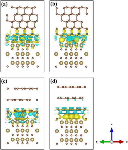
The calculated charge density difference of the diamond or graphite/TaC interfaces is shown in , in which blue cyan and yellow regions represent electron depletion and aggregation, respectively. As shown in , not only there is an obvious charge accumulation between the first layer of C atoms on the top surface of TaC and C atoms on the under surface of diamond, but also there is an obvious charge accumulation between the second layer of Ta atoms on the upper surface of TaC and the C atoms on the under surface of diamond, implying that the C–C covalent bond and C–Ta polar covalent bond are formed. In comparison, there is no charge accumulation between the Ta atoms and C atom of graphite, only the formation of covalent bonds between the carbon atoms. As shown in , the electrons do not overlap between the interfaces and no bonding is formed. This is consistent with the results of the adhesion work.
Figure 4. Charge density differences for fully relaxed Diamond(111)/Tac(111) and Graphite(002)/Tac(111) interfaces, (a) Relaxed-Dia-Model I; (b) Relaxed-Dia-Model II; (c) Relaxed-Gra-Model Ⅴ; (d) Relaxed-Gra-Model Ⅶ.
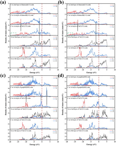
To further understand the bonding information of the diamond or graphite/TaC interfaces, we calculated the partial density of states (PDOS) at the interface, as shown in . It is observed from that the C-2s orbital of diamond forms a clear overlapping peak at –13.2 eV with the C-2s orbital of TaC, while the C-2p orbital of diamond forms a clear overlapping peak at –1.7 eV with the Ta-5d orbital of TaC. These overlapping peaks indicate that C–C and C–Ta covalent bonds are formed between diamond surface and TaC surface. Similarly, we also observe the presence of these two overlapping peaks in the PDOS of the Relaxed-Dia-Model II interface. Moreover, in the energy region around –17.2 eV, the first layer C atoms of TaC at the Relaxed-Dia-Model II interface form overlapping peaks with the first layer C atoms of diamond, which is not present at the Relaxed-Dia-Model I interface. This indicates that the covalent bonds formed at the Relaxed-Dia-Model II interface are stronger, resulting in a greater work of adhesion, which is consistent with the results of the adhesion work. C-Ta strong covalent bond makes Diamond/TaC interface bonding more stable. As can be observed in , there are two overlapping peaks at 2.9 and –9.9 eV, contributed by the 2p orbitals of the C atoms in graphite with the 2p orbitals of the C atoms in TaC and the 2s, 2p orbitals of the C atoms in graphite with the 2s orbitals of the C atoms in TaC, respectively. This indicates that C–C covalent bond is formed between the two layers of carbon atoms. Also, there are no overlapping peaks between the two layers of carbon atoms at the Relaxed-Gra-Model Ⅶ interface in , which indicates that the interface interacts with each other only by van der Waals forces.
Figure 5. Partial density of states (PDOS) for fully relaxed Diamond(111)/Tac(111) and Graphite(002)/Tac(111) interfaces, (a) Relaxed-Dia-Model I; (b) Relaxed-Dia- Model II; (c) Relaxed-Gra-Model Ⅴ; (d) Relaxed-Gra-Model Ⅶ.
4. Conclusion
We deposited nanodiamond films on the silicon substrate using Ta filament by HFCVD. TEM results revealed that TaC transition layer was found to be formed between diamond and substrate, and TaC formed a coherent interface with a special phase relationship: Diamond(111)//TaC(111). First-principles calculated adsorption energy of C atom on the TaC surfaces. The result indicates that C atoms are more likely to adsorb on the TaC (111) C-terminated surface. The structural stability and bonding properties of Diamond/TaC and Graphite/TaC interfaces were further calculated. Diamond(111)/TaC(111) interfacial adhesion work (6.186 J/m2) was much greater than the Graphite(002)/TaC(111) interfacial adhesion work (0.965 J/m2), which indicates that diamond is more stable than graphite on the TaC surface. The results of differential charge and electron density of states show that not only C–C covalent bond but also C–Ta covalent bond are formed, making the Diamond(111)/TaC(111) interface more stable, while only C–C covalent bonds are formed at the Graphite(002)/TaC(111). Our investigations provide critical information to understand the complex diamond formation mechanism, especially with the presence of TaC.
Authors’ contributions
Shaohua Lu: investigation, data curation, writing—original draft, visualization. Xiongtao Zhang: investigation, data curation, writing the original draft. Yuhao Zheng: investigation, data curation. Meiyan Jiang: formal analysis. Chengke Chen: formal analysis. Xiaojun Hu: funding acquisition, conceptualization, supervision, writing—review & editing.
Supplemental Material
Download MS Word (1.3 MB)Disclosure statement
The authors declare that they have no known competing financial interests or personal relationships that could have appeared to influence the work reported in this paper.
Additional information
Funding
References
- Li DM, Hernberg R, Mäntylä T. Catalytic dissociation of hydrogen on a tantalum carbide filament in the HFCVD of diamond. Diamond Relat Mater. 1998;7(11–12):1–9.
- Lee ST, Lin ZD, Jiang X. CVD diamond films: nucleation and growth. Mater Sci Eng R-Rep. 1999;25(4):123–154.
- Schwander M, Partes K. A review of diamond synthesis by CVD processes. Diamond Relat Mater. 2011;20(9):1287–1301.
- Ohmagari S. Single-crystal diamond growth by hot-filament CVD: a recent advances for doping, growth rate and defect controls. Funct Diamond. 2023;3(1):2259941.
- Matsumoto S, Sato Y, Tsutsumi M, et al. Growth of diamond particles from methane-hydrogen gas. J Mater Sci. 1982;17(11):3106–3112.
- Song BK, Kim HY, Kim KS, et al. Unusual dependence of the diamond growth rate on the methane concentration in the hot filament chemical vapor deposition process. Materials. 2021;14(2):426.
- Takamori Y, Nagai M, Tabakoya T, et al. Insight into temperature impact of ta filaments on high-growth-rate diamond (100) films by hot-filament chemical vapor deposition. Diamond Relat Mater. 2021;118:108515.
- Bucknum MJ, Pickard CJ, Stamatin I, et al. On the structure of i-carbon. J Theor Comput Chem. 2006;05(02):175–185.
- Wen B, Zhao JJ, Li TJ. Synthesis and crystal structure of n-diamond. Int Mater Rev. 2007;52(3):131–151.
- Park CG, Yang JW, Hwang NM. TEM observations of metastable nanocarbon allotropes in the initial stage of diamond growth at 300 degrees C during diamond hot filament CVD. Electron Mater Lett. 2023;19(3):316–324.
- Zhu ZG, Jiang CQ, Chen CK, et al. Ordinary-pressure phase transition from graphite to diamond induced by ta atoms. Carbon. 2023;211:118098.
- Zhang CZ, Niakan H, Yang L, et al. Study of diamond nucleation and growth on Ti6Al4V with tungsten interlayer. Surface Coat Technol. 2013;237:248–254.
- Aoki Y, Nakamuta Y, Sugawara Y. Formation of tetrapod-like crystals of diamond formed by hot- filament chemical-vapor-deposition-effects of preformation of tungsten carbide on the substrate. J Cryst Growth. 1995;147(1-2):77–82.
- McNamara KM, Gleason KK. Comparison of tantalum and rhenium filaments in diamond CVD using selective C-13 labeling. J Electrochem Soc. 1993;140(2):L22–L24.
- Jiang MY, Chen CK, Wang P, et al. Diamond formation mechanism in chemical vapor deposition. Proc Natl Acad Sci USA. 2022;119(16):7.
- Li H, Yu QN, Yang B, et al. Electrochemical treatment of artificial humidity condensate by large-scale boron doped diamond electrode. Sep Purif Technol. 2014;138:13–20.
- Ullah M, Rana AM, Ahmad E, et al. Phenomenological effects of tantalum incorporation into diamond films: experimental and first principle studies. Appl Surf Sci. 2016;380:83–90.
- Soto G, Silva G, Contreras O. A study on the flexibility of the hot-filament configuration and its implementation for diamond, boron carbide and ternary alloys deposition. Surf Coat Technol. 2006;201(6):2733–2740.
- Wang SG, Zhang Q, Yoon SF, et al. CVD diamond nucleation enhanced by ultrasonic pretreatment using diamond and mixture of diamond and TaC powders. Diamond Relat Mater. 2002;11(9):1683–1689.
- Kresse G, Furthmüller J. Efficient iterative schemes for ab initio total-energy calculations using a plane-wave basis set. Phys Rev B. 1996;54(16):11169–11186.
- Perdew JP, Burke K, Ernzerhof M. Generalized gradient approximation made simple. Phys Rev Lett. 1996;77(18):3865–3868.
- Stampfl C, Mannstadt W, Asahi R, et al. Electronic structure and physical properties of early transition metal mononitrides: density-functional theory LDA, GGA, and screened-exchange LDA FLAPW calculations. Phys Rev B. 2001;63(15):155106.
- Monkhorst HJ, Pack JD. Special points for Brillouin-zone integrations. Phys Rev B. 1976;13(12):5188–5192.
- Rapcewicz K, Chen B, Yakobson B, et al. Consistent methodology for calculating surface and interface energies. Phys Rev B. 1998;57(12):7281–7291.
- Liu HM, Dandy DS. Studies on nucleation process in diamond CVD – an overview of recent developments. Diamond Relat Mater. 1995;4(10):1173–1188.
- Mandal S. Nucleation of diamond films on heterogeneous substrates: a review. RSC Adv. 2021;11(17):10159–10182.
- Qi Y, Hector LG. Adhesion and adhesive transfer at aluminum/diamond interfaces: a first-principles study. Phys Rev B. 2004;69(23):13.
- Bramfitt BL. The effect of carbide and nitride additions on the heterogeneous nucleation behavior of liquid iron. Metall Trans. 1970;1(7):1987–1995.
- Rose JH, Ferrante J, Smith JR. Universal binding energy curves for metals and bimetallic interfaces. Phys Rev Lett. 1981;47(9):675–678.
- Siegel DJ, Hector LG, Adams JB. First-principles study of metal-carbide/nitride adhesion: al/VC vs. Al/VN. Acta Mater. 2002;50(3):619–631.