
Abstract
To promote the electrocatalytic transformation from CO2 to value-added chemicals with boron doped diamond (BDD) electrode, it is critical to make clear that the relationship between the B doping state and the position of B atom in BDD materials and CO2 reduction performance. Here, a series of BDD electrodes with constant B dopant amount on the surface were prepared by the same process but based on different deposition time (3, 6, 12, and 24 h) using the heat filament chemical vapor deposition. The results demonstrated that the surface grain size, abundances of B–C relative to B–B bonds of the BDD films increased with increasing the deposition time. Moreover, the formic acid yield and faradaic efficiency also increased as well during electrochemical CO2 reduction due to more available B atoms doped in crystallinity (B–C bonds) rather than in grain boundary (B–B bonds) of BDD. Finally, electrochemical analysis revealed that the B–C bonds in the crystal of BDD films is the active sites for the reduction of CO2. This study provides a simple and convenient path to figure out what is the active site of the BDDs and its how to impact the CO2 reduction.
1. Introduction
Nowadays, even increasing attentions to environmental protection and sustainable development have triggered a great interest in the conversion of greenhouse gas CO2 into value-added chemicals [Citation1–3]. As one of promising solution to CO2 conversion, electrocatalytic reduction of CO2 has been extensively studied and large numbers of potential mechanisms have been proposed [Citation4, Citation5]. Compared to metal-based electrodes used widely, boron-doped diamond (BDD) is a powerful candidate, it’s wide potential window in aqueous solution can effectively suppress hydrogen evolution reaction (HER), a competitive side effect for CO2 conversion. High chemical inertness with low adsorption capacity and mechanical durability make it more suitable for practical applications [Citation6–10]. Y. Einaga et al. have demonstrated the validity of BDD electrode for electrocatalytic reduction of CO2 in recent years. Using bare BDD electrode, several typical C1 products such as formaldehyde (HCHO) [Citation8], formic acid (HCOOH) and CO [Citation9] has been obtained, with high selectivity and large faradaic efficiency (FE). These works mainly focused on the effect of extrinsic parameters such as boron doping concentrations, type of electrolytes, cell configuration, working potential applied, and energy input [Citation11–16]. However, the role of intrinsic characteristics, especially the B doping state and the position of B atom in BDD electrode has been little concerned.
In BDD, boron atoms substitute a part of carbon atoms in the tetrahedral crystal structure of diamond, resulting in a transition from insulator to p-type semiconductor and even to metal-like conductor. For p-type BDD electrode, a gradual change from semiconducting properties to a metallic state is observed as the boron doping level ([B]) increases from 1016 cm−3 to 1021 cm−3. 2–3 × 1020 cm−3 is commonly considered as the threshold of semiconducting to metallic [Citation17–20]. Therefore, as the electron acceptor during the CO2 reduction reactions, the electrocatalytic reaction on the BDD electrodes is a very complex process. Several factors, such as boron contents, non-diamond carbon impurities and surface termination, can influence the electrochemical behavior of BDD electrode [Citation7, Citation8, Citation16, Citation19]. Recently, Xu et al. have demonstrated that higher boron content resulted in lower FE for HCOOH [Citation9, Citation20]. In another works, they have shown that when higher boron content is applied, the presence of sp2 carbon species reduces the potential window of the BDD electrode [Citation14, Citation21]. In addition, sp2 carbon directly affects the distribution of the products and HCOOH is the only products on electrodes without sp2 species [Citation13]. Peng et al. found that for sub-microcrystalline BDD electrode, FE for HCOOH production strongly depended on the sp2-bonded carbon content and was almost independent to the boron dopant levels [Citation22].
However, as demonstrated by previous works, B doping could not only endow excellent electrical conductivity of electrode but also affect its morphological and structural features [Citation23]. For example, high boron dopant level could enhance the formation of non-diamond carbon impurities in the grain boundary [Citation24, Citation25]. When precursors with high boron concentrations were used, the dominate facets tend to (111) due to the much slower growth rate in the (111) direction compared to other two directions [Citation26]. Or even higher doping amounts, the number of carriers that contribute to the conductive properties of BDD is limited, which means that not necessarily do all the boron atoms incorporated in the diamond lattice contribute to material conductivity [Citation27]. Meanwhile, the uptake of B atoms was found to be non-uniform across the surface of BDD electrode, and this phenomenon became more obvious at high boron concentration [Citation28]. More importantly, the local coordination of B dopants in heavily BDD electrode would change with the boron contents [Citation26, Citation28]. In this case, it is not sufficient to simply study the influence of boron dopant levels or sp2 species on electrocatalytic reduction of CO2.
As mentioned above, the doping of B affects all aspects of BDD electrode. The previous research has been focused on the influence of the total amount of B on CO2 electrochemical reduction. However, the most critical, the B bonding state and the position of B atom on the surface of BDD film, which has the greatest influence on CO2 electrochemical reduction, have not been studied in depth. In view of this, the effects of the B bonding state and the B distribution in BDD on CO2 electrochemical reduction were reported in this paper. By only changing the deposition time, a series of BDD films with constant B dopant amount on surface but different B–C and B–B bond contents were obtained, and the surface grain size and the grain boundary content on the surface of BDD were analyzed correspondingly. The crystallinity of BDD films characterized by X-ray diffractometer (XRD). The distribution and bonding type of B on the surface were measured by Raman and X-ray photoelectron spectroscopy (XPS). The surface carrier concentration and resistance of the BDD films were performed through Hall-effect test. The electrochemical measurements of BDD electrode were taken to assess their reduction CO2 performances. Finally, the cyclic voltammetry (CV) analysis could be applied to reveal that the B-C bonds in the crystal of BDD films is the active site for reduction of CO2.
2. Experimental
2.1. Preparation of BDD electrode
Poly-crystalline BDD films were prepared by hot filament chemical vapor deposition (HFCVD) reactor on p-type Si (100) substrate. Briefly, the Si substrate was polished with diamond powders (∼ 1 μm) and ultrasonic treated for 30 min to achieve the nucleation sites. The reactive gas source included B2H6, CH4 and H2 (the CH4 ratio was ∼ 3% and the boron to carbon ratio (B/C = 0.017) was introduced into the chamber of HFCVD reactor and the flow rate was set at 400 sccm (standard cubic centimeters per minute at STP). In this condition, the BDD films were deposited for 3, 6, 12, and 24 h (h), respectively.
2.2. Characterization
The plan-view and cross-sectional morphology of BDD films were characterized by field-emission scanning electron microscopy (FESEM, Zeiss Sigma 500). Grazing incident XRD patterns of the samples were obtained using a Philips X'Pert PRO diffractometer, with Cu Ka radiation (λ = l.54 Å) generated by 40 kV, 40 mA electrons as an incident beam in the 2θ range of 35°–145°. Raman spectra were recorded by using an InVia micro-Raman spectrometer (Renishaw, UK) with a 514.5 nm excitation laser. X-ray photoelectron spectroscopy (XPS, ESCALab250, Thermo Fisher Scientific) equipped with a monochromatic K-α radiation source at 1486.6 eV was used to determine the chemical valences of carbon in all BDD films. The sheet carrier concentration and resistance of the films were tested using a Hall effect tester (the Ecopia HMS-3000, Korea).
2.3. Electrochemical measurements
The electrochemical reduction of CO2 was performed in a closed H-type electrolytic cell (Fig. S1) and the electrocatalytic properties was studied with an electrochemical analyzer (760E Instruments, Shanghai Chenhua) in a typical three electrode system using a graphite rod as the counter electrode, and Ag/AgCl (3 mol/L KCl) as the reference electrode. The BDD films acted as working electrodes, which was defined by the sealing organic silica gel (0.64 cm2 area) to prevent the non-electrode area from contact with the electrolyte. The electrolyte of both cathode and anode pool was KHCO3 (0.1 mol/L) aqueous solution and the volumes were 25 mL. Catholyte was saturated by bubbled with CO2 gas for 30 min at 20 sccm. After CO2 saturation, linear sweep voltammetry (LSV) measurements were carried out in the potential range from −3 to 0 V at 0.1 V/s. The BDD electrodes were reduced at −1.7 V versus Ag/AgCl for 2 min and CV at different scan rates (20, 40, 60, 80, 100, and 120 mVs−1) have been obtained in the non-Faradaic region (−0.4 to −0.3 V vs. Ag/AgCl) when the curves of different cycles overlapping. The electrochemical impedance spectra (EIS) of 3, 6, 12, and 24 h BDD electrodes were conducted at a potential of −1.7 V (vs. Ag/AgCl) in the high frequency region from 100 kHz to 0.1 Hz. During reduction, CO2 was continually bubbled into the catholyte at a flow rate of 10 sccm. For determination of evolution rate of gaseous products, the gas outlet of the electrochemical cell was connected to a gas chromatography (GC-2014, Shimadzu Corp.) quipped with a flame ionization detector (FID) and a thermal conductivity detector (TCD) for on-line gas analysis. The liquid product was detected by ion chromatography (CIC-D100, Shine) equipped with an ion chromatographic column (SH-AC-4, 250 mm, 4.6 mm). The calculation formulas of gaseous products and liquid product HCOOH of FE are shown in Eqs. (1)–(4) in supporting information. The amount of HCOOH is calculated by configuring standard HCOOH curves with a series of concentrations, as indicated in Fig. S2.
3. Results and discussion
3.1. Characterization of BDD
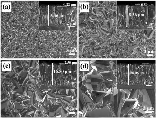
Firstly, the morphology of the crystalline structure was observed from FESEM images of all BDD sample and the deposition time was 3, 6, 12, and 24 h, respectively. As shown in , the crystal possesses well-defined side facets and uniform size with the average grain size increases from 2.28, 3.69, 5.24 to 10.89 μm with increasing the deposition time of BDD films, respectively. In the same geometrical area, the content of grain boundary on the surface decreases conversely. Cross-section FESEM images in the insets of indicates the BDD film comprised of the inverted pyramid shape columnar crystals, and the size of columnar crystal, surface roughness and thickness of the BDD films were gradually increased synchronously. The average roughness and thickness are 0.22, 0.59, 2.50, and 3.36 μm and 5.46, 8.36, 16.80, and 38.06 μm, respectively.
Figure 1. FESEM images of BDD films with the deposited time of (a) 3 h, (b) 6 h, (c) 12 h, (d) 24 h.
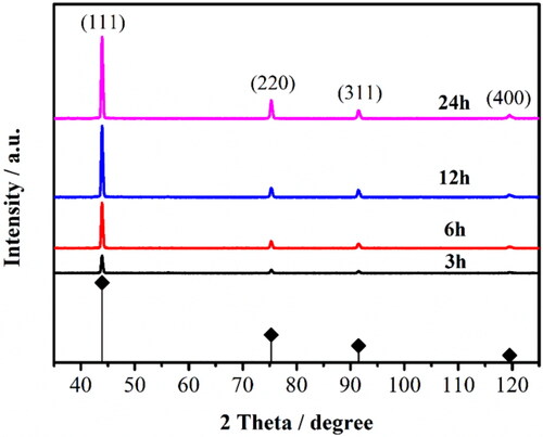
The crystallographic structures and phase purity of the as-prepared BDD films were characterized by XRD (). The pattern confirms the formation of high-quality BDD film and all diffraction peaks can be indexed to the JCPDS card No. 99-0043. The diffraction peaks at 43.93°, 75.3°, 91.50°, and 119.51° are attributed to diffraction of the planes (111), (220), (311) and (400) reflections of the diamond, respectively. Particularly, the sharpest (111) peak of all samples indicated BDD films are (111) plane growth orientation on the surface, and the relative strength of the peaks does not change obviously with increasing the deposition time (Fig. S3), showing that the deposition time does not change the growth orientation but only increase the sizes of the surface grain and columnar crystal of the BDD films.
Figure 2. XRD spectra of BDD films for different deposition time: the black, red, blue, and magenta lines are the test results for 3, 6, 12, and 24 h sample, respectively.
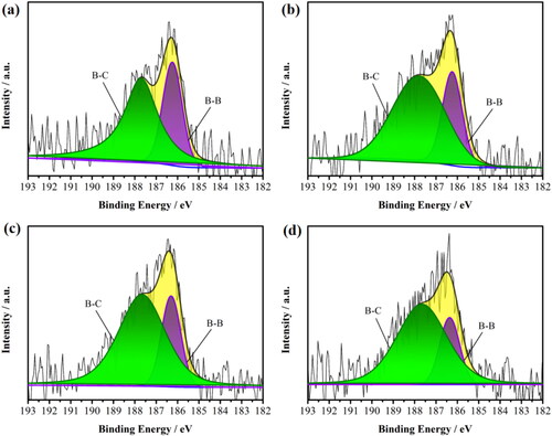
Next, XPS was employed to probe the chemical states of carbon and boron of the BDD films. The high-resolution XPS C1s spectrums for each sample were shown in Fig. S4, all sample were free of impurities and contained only carbon, boron, and oxygen elements. The main peak located at 284.75 eV represents the sp3-C (diamond phase). The peak located at 281.54 eV can be assigned to the sp2-C (graphite phase). The positions at 284.16, 285.1, and 285.72 eV can be attributed to C–H, C–O, and C=O bondings, respectively [Citation29, Citation30]. It can be observed that there is almost no difference for the areas of the four peaks of sp3-C, C–H, C–O, and C=O. Based on the relative percentages of boron and carbon atoms in the XPS peak table (Table S1), the actual B/C ratios of the four samples are 0.019, 0.021, 0.020, and 0.019 (similar to the reactive gas source, B/C = 0.017), respectively. The results demonstrated that the deposition time neither significantly increased the B content on the BDD surface nor changed the content of hydrogen, oxygen terminated states, and diamond phase on the BDD surface. is the XPS deconvolution B 1s energy spectrum of all BDD films. The peaks located at 186.1 and 187.8 eV correspond to B–B and B–C bonds, respectively [Citation31]. The ratio of the two peak areas after fitting was used to quantify the relative content of B-C and B-B bonds on the surface of BDD films. The ratios of the peak areas of B–B and B–C bonds at 3, 6, 12, and 24 h were 0.56, 0.46, 0.33, and 0.29, respectively, indicating that the relative content of the B–B bond decreased significantly with increasing the deposition time.
Figure 3. Deconvoluted XPS B1s spectra for (a) 3 h, (b) 6 h, (c) 12 h, (d) 24 h sample, respectively. The components are shown as follows: (1) B–B (185.92 eV), (2) B–C (187.1 eV).
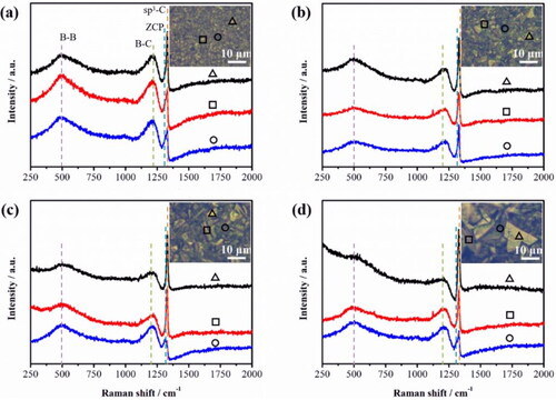
To further understand the distribution state of boron atoms on the surface of BDD films, confocal Raman mapping was performed on different deposition times sample (). The Red, blue and yellow represent sp3-C, B–C, and B–B, respectively. It can be seen that the content of the B–B bonds deceased and the boron is preferentially enriched at the grain boundary to produce boron-rich regions combing the analysis [Citation24, Citation25, Citation32]. In addition, From Raman spectra (), the sharp peak at 1329 cm−1 belongs to the central phonon line in the diamond region (referred to as “ZCP” for short) [Citation33]. Two Lorentz peaks located around 500 and 1200 cm−1, which is derived from the B–B bond and B–C bond vibrations respectively [Citation33, Citation34]. Specifically, the peak around 1540 cm−1, known to be related to sp2 carbon, is not observed in our BDD films [Citation35, Citation36]. Furthermore, the intensity of B–B bonds in the (111) crystal plane (triangles locations) of the BDD films decreased, and the intensity of B–B bonds in the grain boundary (circles locations) of the BDD films increased with increasing the deposition time of BDD films, which consistent with previous reports [Citation35]. Therefore, with increasing the deposition time of BDD films, the total dopant amount of the B remained constant and the grain size on the BDD surface increased, thus, resulting the relative content of the B–B bonds decreased.
Figure 4. Confocal Raman mapping of BDD at different deposition times: (a–e) 3 h; (f–j) 6 h; (k–o) 12 h and (p–t) 24 h. Red, blue, and yellow represent sp3-C, B–C and B–B, respectively. (u) The statistics ratio of the sp3-C, B–C and B–B bonds area based on (b), (g), (i) and (q). (v) The statistics ratio of the B–B/B–C ratio.
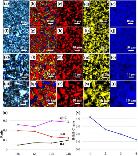
Figure 5. Raman spectra of BDD films at different deposition time: (a) 3 h, (b) 6 h, (c) 12 h, (d) 24 h. The insets are the Raman optical images, and the triangles, circles, and squares represented Raman spectral test locations. The black, red, and blue lines were the test results at triangles, circles, and squares locations, respectively. From the comparison of Raman intensity at square, circular, and triangle points, we can observe that the boron is mainly distributed in the incomplete crystal type region and grain boundary during BDD deposited process.
3.2. Electrical properties
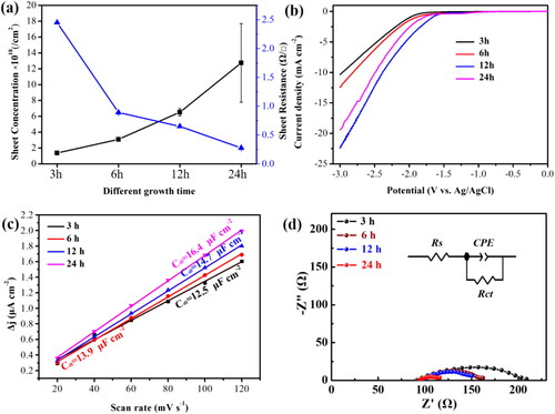
With such geometry, electrical measurements of BDD films were performed with Hall effect method at room temperature, and the sheet concentration and sheet resistance patterns was summarized in a. It can be observed that the sheet concentration was gradually increased and the sheet resistance was gradually decreased with increasing the deposition time, and the average sheet concentration (×1018/cm2) is 1.37, 3.10, 6.51, and 12.74, and the average sheet resistance (Ω/□) is 2.45, 0.89, 0.65, and 0.27 for 3, 6, 12, and 24 h BDD films, respectively. It can be qualitatively concluded that the majority of the B must be present at sites which do not contribute to the continuum of electronic states (giving rise to metallic conductivity and the Fano effects). Such sites may include interstitials, the surface of the crystallites, or bonded within the non-diamond carbon impurities, which present at the grain boundaries [Citation27]. On the other hand, the reasons for the electrical properties of our BDD films were listed as follows: The small contribution of boron atoms at the grain boundary (B–B bonds) and lager boron atoms doped in the crystallinity of BDD films (B–C bonds) with increasing the deposition time.
Figure 6. (a) The sheet concentration and sheet resistance pattern of the BDD films for different deposition time. (b) LSV curve of the BDD elecrodes at different deposition times. LSV was measured by 0.1 V/s in CO2 saturated 0.1 M KHCO3. (c) The double layer capacitance curve with different deposition time of the BDD electrodes. (d) Nyquist plots at a potential of −1.7 V (vs. Ag/AgCl) of the samples.
3.3. Electrochemical reduction of CO2
To reveal the electrocatalytic behavior of the reduction CO2 for BDD electrode, the LSV along with CV analysis were exhibited in b and Fig. S5. The initial potential shifted positively and the reduction starting potential was −1.99, −1.87, −1.74, and −1.60 V (vs. Ag/AgCl) at 3, 6, 12, and 24 h BDD films, respectively, indicating the electrochemical activity of the BDD electrodes gradually increase with increasing the deposition time. The 1/2 slope values of these CV curves were calculated as the double-layer capacitance (Cdl) for BDD electrodes. The Cdl curve of the 24 h BDD electrode (16.4 μF) is largest than the other BDD electrodes (c), implying the electrochemical activity of the BDD electrodes increased with increasing the deposited time. Besides, the EIS of the 3, 6, 12, and 24 h BDD electrodes in the high frequency region are illustrated in d and Table S2, exhibiting that the charge transfer resistance of the BDD electrodes decreased with increasing the deposited time, which means that the B bonding states and the position of B atoms (B–C and B–B bonds) play an extremely important role in electrochemical properties.
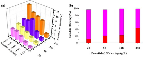
The electrocatalytic performance of different BDD electrodes for CO2 reduction was further investigated by potentiostatic electrolysis in CO2 saturated 0.1 M KHCO3. The range of electrolysis potential was selected from −1.8 to −2.2 V based on the CO2 reduction and hydrogen evolution starting potential of the electrode. a and Table S3 are the HCOOH production rates for 1 h in the electrochemical reduction of CO2 at −1.8 to −2.2 V for different deposition time of BDD electrodes. The reduction products were mainly HCOOH and the production rates of HCOOH increased with the negative shifting of potential. The yield of HCOOH of BDD electrode increased with increasing the deposition time, and the maximal HCOOH yield at 24 h (11.4 μmol cm−2 h−1) was 2.78 times higher than that at 3 h (4.1 μmol cm−2 h−1) @−2.2 V (vs. Ag/AgCl) for the BDD electrode. Therefore, the crystallinity size of the BDD film (via increasing the deposition time) can be effectively improved the yield of HCOOH, indicating that the B–C bonding located inside the crystallinity is the active sites for CO2 reduction [Citation37]. In addition, the FE of the product was also another important index for the electrochemical reduction performance of CO2. b is the FE diagram of CO2 reduction products electrolyzed for 1 h by BDD at −1.9 V with different deposition times. The CO2 reduction products of BDD electrode was only HCOOH and without other by-products (hydrogen competitive reaction). Apart from that, the FE and the selectivity of HCOOH were gradually increased with increasing the deposition time for BDD electrodes, and the maximum FE of HCOOH at 24 h was 43.59%. This is another evidence for the electrochemical CO2 reduction was the B–C bonding of the crystallinity rather than the B–B bonding in the grain boundary of the BDD film.
Figure 7. (a) The production rates of HCOO− obtained from electrochemical reduction of CO2 for 1 h at −1.8 to −2.2 V in 0.1 M KHCO3 by CO2 saturated 30 min. (b) FE for HCOOH (red) and hydrogen (magenta) production for electrochemical reduction of CO2 1h on different deposition times of the BDD electrodes at 3, 6, 12, and 24 h, respectively.
In brief, by changing the deposition time of BDD preparation, the thickness, roughness, grain size, sheet concentration, sheet resistance can be controlled, and the relationship between those parameters and reactivity for CO2 reduction is summarized in Scheme S1. Actually, two factors need to be precisely regulated In order to make clear that the relationship between the B doping state and the position of B atom in BDD materials and CO2 reduction performance: the one is to remain the total B doping amounts on the surface of BDD constant; the other is to change the distribution of the B–B and B–C bonds. In other words, by changing the deposition time of BDD preparation and keep the reactive gas source B/C = 0.017, the columnar crystal increase and the grain boundary decrease, thus resulted both the thickness and roughness of the BDD film increase [Citation38]. Which mean that the B–C bonds located in crystallinity of BDDs increase and the B–B bonds located in grain boundary decrease, and the B–C bonds are the active sites for CO2 reduction.
4. Conclusions and perspectives
In summary, a series of BDD films of the same B dopant amount (B/C ratios ∼ 0.019) on the surface were fabricated by HFCVD method with the relative abundances of B–B bonds and B–C bonds of the four samples ranging from 0.56 to 0.29. The as-prepared BDD electrodes were found to demonstrate certain trends that the average thickness, roughness, grains size, sheet concentration (×1018/cm2) increased from 5.46 to 38.06 μm, 0.22 to 3.36 μm, 2.28 to 10.89 μm, 1.37 to 12.74, and the sheet resistance (Ω/□) decreased from 2.45 to 0.27 with increasing the deposited time, respectively. Finally, electrochemical analysis was conducted to study about the CO2 reduction performance on these BDD working electrodes and the best performance for producing HCOOH yield and FE from CO2 was found on the 24 h BDD electrode with the maximum FE is 43.59%. From the structural characterization and the electrochemical measurements of BDD electrodes, we could observe that the deposition time can effectively improve the size of the inverted pyramid shape columnar crystals and the surface grain size, thus resulting more available B–C bonds (active sites) on the same area of the BDD electrodes for CO2 reduction. Therefore, it was noteworthy that this study provides a new idea for further improve the HCOOH production for BDD electrodes.
BDD materials have revealed great potential for the electrochemical CO2 reduction. The catalytic performance of BDD is known to be influenced by the type/concentration of B dopants, the surface terminations and functionalities, the crystallinity, the defect sites and the sp2 non-diamond carbon contents, etc. However, the product selectivity and reduction efficiency are limited by the selection of microorganisms and the harsh cultivation environments. Particularly, the obtained masses of products are relatively small. There still exists a big gap from the laboratory research to large-scale industrial application of CO2 reduction. The main challenges for the industrial CO2 reduction process using BDD materials include the design of reactors, the exploration of catalysts with improved performance and the selection of suitable electrolytes. Therefore, more studies still need to be conducted regarding the relationship between the physical, chemical, and electronic features of BDD and its catalytical activity for CO2 reduction in the future.
Authors’ contributions
Huiqiang Liu: Methodology, Validation, Investigation, Writing-original draft. Xiangyan Cheng: Validation, Investigation, Writing-original draft. Jiajun You: Validation, Investigation. Baohua Zhang: Validation, Investigation. Bing Wang: Conceptualization, Methodology, Funding acquisition. Lin Chen: 2D-mapping measurements, Writing-original draft. Ying Xiong: Conceptualization, Funding acquisition, Investigation, Methodology, Project administration, Methodology, Supervision, Validation, Writing-review & editing.
Supplemental Material
Download MS Word (1.5 MB)Disclosure statement
The authors declare that they have no known competing financial interests or personal relationships that could have appeared to influence the work reported in this paper.
Additional information
Funding
Notes on contributors
Huiqiang Liu
Xiangyan Cheng, Jiajun You and Baohua Zhang are the master students, Huiqiang Liu and Lin Chen are associate professors, Bing Wang and Ying Xiong are the professors in Southwest University of Science & Technology.
Huiqiang Liu: Data Curation, Formal analysis, Writing - original draft, Writing - review and editing. Xiangyan Cheng: Investigation, Formal analysis; Writing - review and editing. Jiajun You: Data curation, Visualization. Baohua Zhang: Formal analysis. Bing Wang Writing - review and editing. Lin Chen: Investigation, Formal analysis, Supervision, Writing - review and editing. Ying Xiong: Conceptualization, Investigation, Formal analysis, Supervision, Data Curation, Writing - original draft, Writing - review and editing.
References
- Dattila F, Seemakurthi RR, Zhou Y, et al. Modeling operando electrochemical CO2 reduction. Chem Rev. 2022;122(12):1–9.
- Watanabe T, Pfeil-Gardiner O, Kahnt J, et al. Three-megadalton complex of methanogenic electron-bifurcating and CO2-fixing enzymes. Science. 2021;373(6559):1151–1156.
- Navarro-Jaén S, Virginie M, Bonin J, et al. Highlights and challenges in the selective reduction of carbon dioxide to methanol. Nat Rev Chem. 2021;5(8):564–579.
- Li L, Li X, Sun Y, et al. Rational design of electrocatalytic carbon dioxide reduction for a zero-carbon network. Chem Soc Rev. 2022;51(4):1234–1252.
- Xue Y, Feng X, Roberts SC, et al. Diamond and carbon nanostructures for biomedical applications. Funct Diamond. 2021;1(1):221–242.
- Natsui K, Iwakawa H, Ikemiya N, et al. Stable and highly efficient electrochemical production of formic acid from carbon dioxide using diamond electrodes. Angew Chem Int Ed. 2018;57(10):2639–2643.
- Ganiyu SO, Dos SV, Martínez-Huitle CA, et al. Opportunities and challenges of thin-film boron-doped diamond electrochemistry for valuable resources recovery from waste: organic, inorganic, and volatile product electrosynthesis. Curr Opin Electrochem. 2022;32:100903.
- Luo D, Ma D, Liu S, et al. Electrochemical reduction of CO2 on fluorine-modified boron-doped diamond electrode. Diam Relat Mater. 2022;121:108753.
- Xu J, Natsui K, Naoi S, et al. Effect of doping level on the electrochemical reduction of CO2 on boron-doped diamond electrodes. Diam Relat Mater. 2018;86:167–172.
- Chen Y, Gao X, Liu G, et al. Correlation of the role of boron concentration on the microstructure and electrochemical properties of diamond electrodes. Funct Diamond. 2021;1(1):197–204.
- Jiwanti PK, Einaga Y. Electrochemical reduction of CO2 using palladium modified boron-doped diamond electrodes: enhancing the production of CO. Phys Chem Chem Phys. 2019;21(28):15297–15301.
- Verlato E, Barison S, Einaga Y, et al. CO2 reduction to formic acid at low overpotential on BDD electrodes modified with nanostructured CeO2. J Mater Chem A. 2019;7(30):17896–17905.
- Tomisaki M, Kasahara S, Natsui K, et al. Switchable product selectivity in the electrochemical reduction of carbon dioxide using boron-doped diamond electrodes. J Am Chem Soc. 2019;141(18):7414–7420.
- Xu J, Einaga Y. Effect of sp2 species in a boron-doped diamond electrode on the electrochemical reduction of CO2. Electrochem Commun. 2020;115:106731.
- Ivandini TA, Watanabe T, Matsui T, et al. Influence of surface orientation on electrochemical properties of boron-doped diamond. J Phys Chem C. 2019;123(9):5336–5344.
- Souza FL, Lopes OF, Santos EV, et al. Promoting CO2 electroreduction on boron-doped diamond electrodes: challenges and trends. Curr Opin Electrochem. 2022;32:100890.
- Umezawa H, Takenouchi T, Kobayashi K, et al. Growth of heavily boron-doped polycrystalline superconducting damond. New Diamond Front Carbon Technol. 2007;17(1):1–9.
- Yamada H, Shimaoka T. Study of horizontal and vertical uniformity of B-doped layer on mosaic single crystal diamond wafers by using hot-filament chemical vapor deposition. Funct Diamond. 2022;2(1):46–52.
- Zhu R, Liu F, Deng Z, et al. Inconsistency of BDD reactivity assessed by ferri/ferro-cyanide redox system and electrocatalytic degradation capability. Funct Diamond. 2022;2(1):71–79.
- Xu J, Yokota Y, Wong RA, et al. Unusual electrochemical properties of low-doped boron-doped diamond electrodes containing sp2 carbon. J Am Chem Soc. 2020;142(5):2310–2316.
- Einaga Y, Foord JS, Swain GM. Diamond electrodes: diversity and maturity. MRS Bull. 2014;39(6):525–532.
- Peng Z, Xu J, Kurihara K, et al. Electrochemical CO2 reduction on Sub-microcrystalline boron-doped diamond electrodes. Diam Relat Mater. 2021;120:108608.
- Zeng X, Zhao Y, Chen N, et al. Analysis on electrochemical CO2 reduction by diamond doping technology. J Electrochem En Conv Stor. 2023;20:020801.
- Watanabe T, Yoshioka S, Yamamoto T, et al. The local structure in heavily boron-doped diamond and the effect this has on its electrochemical properties. Carbon. 2018;137:333–342.
- Wilson NR, Clewes SL, Newton ME, et al. Impact of grain-dependent boron uptake on the electrochemical and electrical properties of polycrystalline boron doped diamond electrodes. J Phys Chem B. 2006;110(11):5639–5646.
- May PW, Ludlow WJ, Hannaway M, et al. Boron doping of microcrystalline and nanocrystalline diamond films: where is the boron going? MRS Proc. 2007;1039(1):1703.
- Manciu FS, Manciu M, Durrer WG, et al. A drude model analysis of conductivity and free carriers in boron-doped diamond films and investigations of their internal stress and strain. J Mater Sci. 2014;49(16):5782–5789.
- Pleskov YV, Krotova MD, Evstefeeva YE, et al. Synthetic semiconductor diamond electrodes: comparison of electrochemical impedance at the growth and nucleation surfaces of a coarse-grained polycrystalline film. Russ J Electrochem. 2001;37(11):1123–1127.
- Lu C, Tian SB, Gu CZ, et al. Grain boundary effect on the superconducting transition of microcrystalline boron-doped diamond films. Diam Relat Mater. 2011;20(2):217–220.
- Pleskov YV, Evstefeeva YE, Krotova MD, et al. Synthetic semiconductor diamond electrodes: the comparative study of the electrochemical behaviour of polycrystalline and single crystal boron-doped films. J Electroanal Chem. 1998;455(1-2):139–146.
- Pleskov YV. New corrosion-resistant electrodes: synthetic diamond and diamond-based materials. The semiconductor and structure aspects-a review. Prot Met. 2006;42(2):103–118.
- Yang H, Ma Y, Dai Y. Progress of structural and electronic properties of diamond: a mini review. Funct Diamond. 2022;1(1):150–159.
- Szunerits S, Mermoux M, Crisci A, et al. Raman imaging and Kelvin probe microscopy for the examination of the heterogeneity of doping in polycrystalline boron-doped diamond electrodes. J Phys Chem B. 2006;110(47):23888–23897.
- Ullah M, Ahmed E, Hussain F, et al. Electrical conductivity enhancement by boron-doping in diamond using first principle calculations. Appl Surf Sci. 2015;334:40–44.
- Wächter N, Munson C, Jarošová R, et al. Structure, electronic properties, and electrochemical behavior of a boron-doped diamond/quartz optically transparent electrode. ACS Appl Mater Interfaces. 2016;8(42):28325–28337.
- May PW, Ludlow WJ, Hannaway M, et al. Raman and conductivity studies of boron-doped microcrystalline diamond, facetted nanocrystalline diamond and cauliflower diamond films. Diam Relat Mater. 2008;17(2):105–117.
- Bard AJ, Faulkner LR. Electrochemical methods: fundamentals and applications, New York: Wiley, 2001, 2nd ed. Russ J Electrochem. 2002;38:1364–1365.
- Long H, Hu H, Wen K, et al. Thickness effects on boron doping and electrochemical properties of boron-doped diamond film. Molecules. 2023;28(6):2829.