
 ?Mathematical formulae have been encoded as MathML and are displayed in this HTML version using MathJax in order to improve their display. Uncheck the box to turn MathJax off. This feature requires Javascript. Click on a formula to zoom.
Abstract
We investigated the correlation between microstructures and optical properties of boron ion implanted microcrystalline diamond (B-MCD) thin films annealed at different temperatures. Ellipsometry characterization of B-MCD films was performed in the wavelength range of 380–1000 nm and the disperse parameters of the films such as single oscillator energy and dispersive energy were uniquely determined by using a Gaussian model. The results show that the refractive index increases from 2.18 to 2.21 to 2.28–2.29 with annealing temperature increasing from 700 to 800 °C and then it slightly decreases to 2.25–2.28 with annealing temperature further increasing to 900 °C, implying that the annealing temperature has a significant impact on the optical properties of B-MCD films. Raman spectra reveal that the full width at half maximum of diamond peak significantly decreases after 800 °C annealing, indicating a better quality of diamond crystalline. X-ray photoelectron spectroscopy results show that this sample contains higher sp3 carbon content, lower sp2 and C–O contents on the film surface after 800 °C annealing, implying that fewer defects exist. The results are of great significance for the preparation of excellent boron ion implanted microcrystalline diamond for waveguide based Mach-Zehnder Interferometer liquid sensing.
1. Introduction
Real-time monitoring on food processing lines plays an important role in ensuring food safety. The most common liquid phase sensor was supposed to be the mid-infrared attenuated total reflection sensor (ATR) currently [Citation1–3]. Generally, ATR unit was mainly made of silicon or germanium materials, which was poor corrosion-resistant as well as bad chemical stability, gradually deteriorating the performance and service life of the devices [Citation4–6]. Diamond has good corrosion resistance, biocompatibility, high optical transparency and unique integrated photonic structure, which embraced a promising prospect in the application fields of bio-sensor and food safety detection [Citation7,Citation8]. Recently, polycrystalline or nanocrystalline diamond film based waveguides had been applied in ultra-high frequency optical mechanical signal processing systems [Citation9–11] or thermo-optical tunable filters [Citation12]. However, there is few reports about the preparation of diamond films-based waveguide in mid-infrared liquid phase sensor.
ATR system receives the test result by analyzing the signals, which are respectively collected from the solvent (backgrounds) and solutions. For the absorption spectrum is strongly correlated with temperature, the changes of temperature between two recording spectra made huge changes from background signals, which brings big errors of data. The Mach-Zehnder Interferometer (MZI) measurement system, who is a two-arm measurement system, one for the sample and the other for the reference solvent, is different from the traditional ATR unit. When the signal from the same light source passes through the two arms, the signals of the solvent and solution will be collected at nearly the same temperature, and they will interfere at the output end. By analyzing the interference signal, we can get the test results. In this case, MZI avoids the errors from the two separate tests and effectively improves the detection accuracy [Citation13]. Meanwhile, it can also greatly reduce the volume of the equipment and realize online real-time detection. However, there always is a slight difference in length between the two arms, leading to a phase difference and impacting the interference signal. It is necessary to prepare a phase shifter on the MZI arm and adjust the refractive index to tune the phase difference. Therefore, it is an urgent task to design a high effective and sensitive phase shifter to adjust the phase by tuning the refractive index.
It was reported that the phase had been modulated by coupling a photonic crystal resonator on the MZI reference arm or signal arm [Citation9–11]. This method has a complicated process with high power consumption. Another way to adjust the refractive index is designed based on thermo-optical effect, in which refractive index varies with the temperature. Some researchers realized the thermo-optical effect by pasting a heater or depositing a resistance layer on MZI single arm to adjust its refractive index and phase [Citation12]. These methods had complex processes and were difficult to achieve precise control. Conductive diamond is regarded as necessary for thermo-optical effect. At present, boron doped diamond films prepared during the growth process or boron ion implantation normally exhibited good electrical properties [Citation14,Citation15]. However, it was found that when the doping concentration in CVD diamond films was high, the internal structure was destroyed, and the optical properties were significantly reduced, which was not conducive to prepare optical devices [Citation16]. Meanwhile, boron ion implantation inevitably introduced some defects in the film, greatly destroyed the crystal lattice, and even caused a large amount of graphite and sp2 carbon in the film. This thereby produced local fluctuations in dielectric constant, decreasing the value of complex refractive [Citation17–19]. These adverse effects greatly reduced the performance of the waveguide.
It is suggested that the B+-implanted MCD films that simultaneously possess good electrical and optical properties, can form an efficient local micro-heater and achieve precise control of the refractive index, realizing thermo-optical type MZI. Also, boron ion doping with varied doses affects the optical properties of MCD films, and it is a means to adjust the refractive index. However, it cannot regulate the refractive index in real-time. So, it is still necessary to use thermal-optic effect to adjust the refractive index in real-time monitoring. As a result, the effects of B+ implantation on the optical properties of diamond films are the first issue to be studied. Our previous results showed that vacuum annealing had a significant role in improving the microstructure of the film. Nevertheless, the influences of annealing temperature (Ta) on the optical properties of diamond films has not yet been reported. Here, we implanted B+ into MCD films and performed annealing treatments at different temperatures. The effects of annealing on the optical properties of the film are studied, which is the base to prepare the thermo-optic phase shifter and has a great significance in the future to develop the research on the thermal-optic effects and to realize the application of diamond in liquid phase sensors.
2. Materials and experiments
The MCD films were prepared on a high-resistance single crystal silicon (100) substrate by using HFCVD. The carbon source was acetone (CH3COCH3); hydrogen was used to bring the acetone into the chamber and this part of hydrogen flow was named carbon source flow; the working pressure in the reaction chamber was 3.5 kPa; the substrate temperature fluctuated in the range of 840–855 °C; the gas mixture consisted of CH3COCH3 and H2, the extra added hydrogen flow rate was a constant value of 200 sccm, and the film were prepared at a growth rate of 0.5 µm/h. MCD thin films were implanted with 100 keV boron ion up to 1 × 10¹⁵ B/cm2 at room temperature on line 1 of DF implanter at Surrey Ion Beam Centre. The sample was 7 degrees titled again the beam, and beam was scanned well over an area defined by a round aperture with two-inch diameter. The estimated implantation range of 100 keV B+ in MCD is about 157 nm. B+ implanted samples were annealed in vacuum at 700, 800 and 900 °C for 30 min, named as MCD-B-700, MCD-B-800 and MCD-B-900, respectively. The samples without boron ion implanted and annealing were set as contrast samples and named as Un-implanted and As-implanted, respectively.
The microstructures of films are investigated by field emission scanning electron microscopy (FESEM, FEI nova450) and atomic force microscopy (AFM, Bruker Dimension), and figures are provided with a magnification of 50k times for overall morphology SEM. Meanwhile, the icon ruler of AFM is exhibited 5 µm × 5 µm. Visible Raman spectroscopy measurements (Renishaw inva Reflex) were performed to analyze the phase composition of the film with an excitation laser of 532 nm at room temperature. The various chemical bonding information of different annealing temperature samples were characterized by XPS (Axis Ultra DLD spectrometer). Complex refractive index of samples was measured by a ME-L Mueller matrix ellipsometer (Wuhan Optics Technology Co, Wuhan, China) in a wavelength range from 380 to 1000 nm, and the measuring angle closes to the Brewster angle of 65° ± 0.1°.
3. Results and discussion
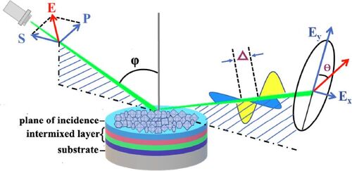
shows the schematic illustration of the matrix ellipsometer process of MCD films. The electric field of the incident beam has two perpendicular components. P-light is parallel to the direction of vibration of the light wave, while the S-light is vertical to the vibration direction of the light wave. We performed ellipsometer spectroscopy (SE) measurements at room temperature with an incident angle of 65° and a wavelength range of 380–1000 nm.
Figure 1. Schematic illustration of the possible modes for matrix ellipsometer processes of MCD films.
According to the Fresnel formula [Citation20], the measured value of amplitude ratio () and phase shift (Δ) of parallel (
) for the SE are the polarization change of the incident light after the light is reflected. Expressed as the ratio of the parallel component (rp) and the vertical component (rs). The ratio ρ of the polarized light is defined as EquationEquation (1)
(1)
(1) [Citation21].
(1)
(1)
In EquationEquation (2)(2)
(2) , the relationship between the complex dielectric function (𝜉) and the complex refractive (n-k) index is defined, where the 𝜉1 and 𝜉2 symbolize the real and imaginary parts of dielectric constants, respectively, and φ is the angle of incidence [Citation22].
(2)
(2)
Since in SE method, presentation of an optical model is necessary and the dielectric function of the samples are not known, a standard model consists of a silicon substrate, diamond thin film, boron ion implanted layer, surface roughness layer and air as the ambient medium was designed shown in . The thickness of intermixed layer was set as 500 nm for samples in this study. The optical responses of roughness and intermixed layers were estimated using effective medium approximation (EMA). In the modeling step in accordance with the selected material, the proper dispersion formula was used to describe the optical dispersion constants of the thin film. In experiments, φ and Δ are measured as a function of wavelength. Based on the model we built and the function we obtained, fitting parameters were chosen and Gaussian model was used in this work [Citation23].
(3)
(3)
where the Amp represents the amplitude (eV), En0 (eV) is peak position, and Br (eV) is peak bandwidth.
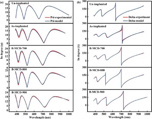
shows the experimental results and values of angles (φ, Δ) across the full wavelength range. It is observed that the spectrum exhibits oscillatory properties due to the interference effect of light, indicating that the films have good optical transparency. The frequency of the oscillation depends on the thickness of the film. Generally, larger film thickness leads to higher frequency, and the electronic transitions in the MCD film leads to the occurrence of light absorption.
Figure 2. Experimental and fitted values of φ and Δ values for samples with Un-implanted, As-implanted, B-MCD-700, B-MCD-800 and B-MCD-900, respectively.
shows the variation of refractive index (n) and the extinction coefficient (k) for the MCD films, which is obtained from the fitted parameters information from (a). According to EquationEquation (2)(2)
(2) , the n and k values are related to the complex dielectric constant. The index n depended on the chemical composition of the material, while the coefficient k characterized the attenuation of light energy or dissipation of incident photon energy within material [Citation24,Citation25], which was affected by the defects in the material. shows the n-k values of Un-implanted and As-implanted samples, revealing that refractive index would be lowered by ion implantation. (c) shows that the refractive index value increases to 2.18–2.21 after annealing at 700 °C, higher than the maximum n value of As-implanted samples (2.18). (d) displays that the optical constants of films have a high refractive index, approaching to that of natural diamond (2.45), indicating that 800 °C annealing can enhance the bond of lattice structure and more closely packed crystals. As can be seen from (e), when annealing temperature increases to 900 °C, the value of n is lower than that of the B-MCD-800 sample, and gradually decreases to 2.25–2.28. It is observed that the index k of the thin films is 0.08–0.05, 0.14–0.07, 0.11–0.06, 0.11–0.04, and 0.09–0.05 for samples of Un-implanted, As-implanted, B-MCD-700, B-MCD-800 and B-MCD-900, respectively, indicating that k values of the MCD films decrease with increasing wavelength, which is related to the absorption coefficient α (α = 4kπ/λ). More importantly, the k values in samples of B-MCD-700, B-MCD-800 and B-MCD-900 are lower than that of As-deposited, which is more likely to improve the optical transmittance in diamond films. This suggests that reasonable Ta improves the optical properties of B+-implanted diamond films.
Figure 3. The variation of index of refraction (n) and extinction coefficient (k) with incident wavelength and photo energy for samples (a) Un-implanted, (b) As-implanted, (c) B-MCD-700, (d) B-MCD-800 and (e) B-MCD-900, respectively. FESEM micrographs and corresponding AFM three-dimensional stereographs of samples (f-F) Un-implanted, (g-G) As-implanted, (h-H) B-MCD-700, (i-I) B-MCD-800 and (j-J) B-MCD-900, respectively.
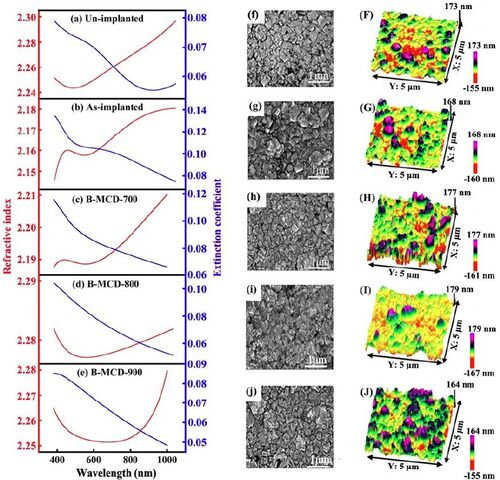
Combining the optical constant () obtained from SE, we find that the refractive index of the B-MCD-700 has been significantly improved compared with the unannealed sample (As-implanted). With the Ta further increasing to 800 °C, the refractive index value of B-MCD-800 reaches to a value close to that of natural diamond, while that of B-MCD-900 begins to decrease. It is revealed that the annealing temperature of films plays a key role for diamond optical properties.
To understand the dependence of optical properties on the boron ion implanted and annealing, we characterized the surface and structure feature of the samples after boron ion implanted as well as different temperature annealing for 30 min by using FESEM and AFM. As shown in , the films are compact and possess well continuity with an average grain size about 200 ∼ 300 nm. (f) shows the surface morphology of the Un-implanted diamond film. It is observed that the diamond film is composed of irregular micro sized blocky structures. (g) shows that there are some polymers on the surface of the As-implanted sample, which is attributed to the large surface sputtering during boron ion implantation for the high ion dose [Citation26]. As shown in , it is found that the surface morphology of annealed samples B-MCD-700, B-MCD-800 and B-MCD-900 nearly keep unchanged comparative with that of the Un-
implanted sample. This suggests that the annealing restores to some extent the surface damage produced by boron ion implantation.
The corresponding AFM pictures of SEM graphs show that the As-implanted sample exhibits a nearly flat surface and some heaves appear after boron ion implanted, see (G). It is noted that in (H), more heaves appear after 700 °C annealing, indicating that the surface becomes rougher. As shown in (I), the heaves become larger hills, suggesting that the roughness further increases in the case of 800 °C annealing. With the annealing temperature increasing to 900 °C ((J)), some hills become sharp, revealing that there are some components in the surface disappear.
lists the values of thickness, roughness and EMA from SE test fitting information and the data of Ra and Rq obtained from AFM. Because SE is very sensitive to the structure of the film, in general, lower surface roughness and thickness can improve the accuracy of the physical fitted values [Citation27]. It is observed that the film effective thickness is about 475 nm, and the SE model roughness is similar with the Ra values, illustrating that the model data are reasonable. We also have estimated the EMA of non-uniformity layer. EMA of the As-implanted sample is smaller than that of the Un-implanted sample and other annealed samples. With Ta increasing to 900 °C, the value of EMA gradually increases from 34.1 nm to 46.4 nm. It is also observed that for the As-implanted sample, Ra = 30.8 nm and Rq = 40.0 nm, which is all lower than that of other samples. This reveals that boron ion implantation decreases the roughness, which is in agreement with that of the model results. This phenomenon can be elucidated by the mechanism that carbon vacancies in individual grains in As-implanted films will be replaced by implanted boron ions, resulting in decrease of the roughness after boron ion implantation. When Ta increases to 800 °C, the Ra and Rq values rise to 35.8 nm and 47.1 nm, respectively. As Ta further increases to 900 °C, the values of Ra and Rq gradually increase from 34.7 nm to 37.0 nm and 44.8 nm to 48.0 nm, respectively, according to the AFM graphs. It is also noted that the results of roughness from SE is in good agreement with those from AFM. Meanwhile, When Ta increases to 800 °C, the grain arrangement on the surface is more uniform, and the grain height difference on the surface of the thin film is smaller. There is no large amount of air (refractive index of about 1) filling between the grains, so the refractive index value of B-MCD-800 reaches the highest.
Table 1. The values of thickness, roughness and EMA from SE test fitting information and the data of Ra and Rq obtained from AFM.
To further understand the phase composition at different Ta, we performed visible Raman spectroscopy measurements in the range of 1000–1800 cm−1 for each sample, as shown in (a). The Raman spectra were well fitted with six Gaussian-Lorentzian peaks. It is clearly observed that fitted peaks are located at 1130–1160 cm−1, 1230–1250 cm−1, 1332–1334 cm−1, 1350 cm−1, 1460–1480 cm−1 and 1550–1580 cm−1, respectively. The peaks at 1130–1160 cm−1 and 1460–1480 cm−1 are related to trans-polyacetylene (TPA) oligomers, which are expressed to C-H/C-C bending modes of bending and stretching of TPA in amorphous carbon grain boundaries (GBs) of MCD films [Citation15,Citation28]. The peaks at 1350 cm−1 and 1550–1580 cm−1 corresponding to the D and G bands, which are related to sp2 graphitic phase [Citation29,Citation30]. The peak at about 1332–1334 cm−1 is related to diamond phase, while that the 1250 cm−1 originates from amorphous sp3 carbon GBs of the films [Citation31,Citation32]. The diamond peak intensity sharpens with increasing annealing temperature, indicating that diamond contents increase and the damage from boron ion implanted is recovered.
Figure 4. (a) Typical visible Raman spectra from Un-implanted, As-implanted, B-MCD-700, B-MCD-800 and B-MCD-900 samples, (b) the ratio of ITPA/ISUM and ID/IG values, (c) the diamond peak position and its FWHM values, and (d) the G band position and its FWHM.
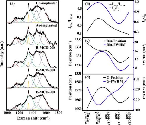
The evolutions of the intensity ratio of the D peak to G peak (ID/IG) values have been summarized in (b). It is generally proportional to estimate the size and number of sp2 carbon clusters in GBs [Citation33]. The ID/IG value of the As-implanted sample is the highest (1.18), which becomes the lowest (0.55) with Ta increases to 800 °C, indicating the sp2 carbon clusters are the smallest in 800 °C annealed sample. When Ta increases to 900 °C, it increases to a higher value of 0.88. These results indicate that the sp2-bonded carbon content located in the films decreases at 700–800 °C and then it increases at 900 °C.
(b) shows the calculated values of ITPA/ISUM (the peak area of 1140 cm−1 and 1470 cm−1 to all peaks). The ITPA/ISUM value of the Un-implanted sample (0.23) is lower than that of the As-implanted sample (0.38). It is also observed that the value continues to decrease with the increase of Ta. When the sample was annealed at 900 °C, the ITPA/ISUM ratio further decreases to 0.23. This suggests that the chains of TPA might be destroyed and hydrogen atoms start to desorb at such a high annealing temperature. Due to the fact that TPA phases were mainly embedded in amorphous carbon GBs [Citation34,Citation35], the number of GBs is reduced correspondingly. This reveals that the increasing of Ta is beneficial to reduce the content of amorphous carbon GBs.
Diamond peak position and its FWHM values with different Ta are shown in (c). It is observed that when Ta is lower than 800 °C, diamond peak position shows a red shift. When Ta is higher than 800 °C, diamond peak position shows a blue shift. For sample B-MCD-800, the diamond peak position is very close to that of prefect diamond of 1332 cm−1, and its FWHM value is 7.08 cm−1, which is significantly lower than that of Un-implanted (14.9 cm−1), As-implanted (13.8 cm−1), B-MCD-700 (7.8 cm−1) and B-MCD-900 (9.1 cm−1). This indicates that the grain-induced repair ability of the film is the strongest under 800 °C annealing. When Ta increases to 900 °C, the peak position and FWHM values are both significantly elevated. This indicates that the microstructure of sample B-MCD-800 is better than that of samples Un-implanted, As-implanted, B-MCD-700 and B-MCD-900, revealing that the diamond in B-MCD-800 has the highest quality after 800 °C annealing.
(d) represents G peak position and the evolution of FWHM values for the As-implanted and 700–900 °C annealed samples. It is observed that the values of G-position nearly keep constant in reference to As-implanted and B-MCD-700 samples. With the temperature increasing to 800 °C, the FWHM value significantly increases from 105 to 121 cm−1, and the position of G peak moves from 1571 to 1557 cm−1. Referring to (b), ID/IG value decreases to the lowest value when annealed at 800 °C. This implies that the graphitic clusters become smaller and sp2 carbon arrangement is more disordered at 800 °C [Citation35].
Considering all the Raman information, we can conjecture that several possible factors affect optical performance. For the three annealed samples, as the Ta increases from 700 to 800 °C, the refractive index range increases from 2.18–2.21 to 2.28–2.29 and decreases to 2.25–2.28, suggesting that the 800 °C annealing can reduce the defect and optimize the lattice structure, which greatly improves the optical properties. For the sample of B-MCD-800, we can find noteworthy information that ID/IG and its FWHM values of diamond peak both decrease to the lowest, indicating that the quality of diamond grains is the best and the number of sp2 carbon clusters is the lowest than that of other samples, revealing that the suitable annealed Ta can reduce the sp2 carbon content and optimize the lattice structure, which dramatically improves the optical properties.
To further understand the dependence of optical properties on the annealing temperatures, we used XPS to analyze the various chemical bonding information of different annealing temperature samples. The data of XPS deconvoluted the C1s spectra by using a mixed Lorentzian-Gaussian product function, determined C1s core-energy level spectra of samples. As shown in , C1s spectra peaks are located at 284.8, 285.2, 286.3, 287.0 and 288.8 eV, which are corresponding to sp2 C = C, sp3 C–C, C–O, C = O and π-π*, respectively [Citation36]. It should be noted that the presence of oxygen atoms content is mainly from the carbon source (CH3COCH3) during CVD system and the annealing atmosphere.
Figure 5. Typical C1s core-energy level spectra and boron ion implanted samples after annealing at different temperature.
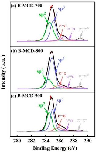
The content of chemical bonds from C1s spectra is calculated according to the fitted data in . It indicates that chemical composition of sp3 carbon content in samples B-MCD-700 (36.7%) and B-MCD-900 (43.9%) are lower than that of B-MCD-800 (52.7%). Meanwhile, the sp2 carbon content in samples of B-MCD-700 (44.2%) and B-MCD-900 (39.1%) are higher than of B-MCD-800 (29.5%). The results indicate that sp3 carbon content in the films increases and some amorphous carbon disappear when Ta increasing to 800 °C. This also confirmed the Raman spectroscopy conclusions of ID/IG value decrease. By combining the evolution of complex refractive index from , it is suggested that the optical properties of diamond films are dramatically improved with higher concentration of diamond phase.
Meanwhile, we can find the chemical bond composition information of C–O and C = O bonds in the samples annealed at different temperatures from XPS spectra. The results show that the content of C–O bonds decreases from 4.5% (700 °C) to 3.9% (800 °C) and then increases to 4.2% (900 °C) and that of C = O bonds are increasing from 5.2% (700 °C) to 7.7% (800 °C) to 10.6% (900 °C) when annealing temperature increases from 700–900 °C. It is obvious that the content of C–O bonds in samples B-MCD-700 and B-MCD-900 is higher than that of B-MCD-800. The C–O bonds are a kind of sp3 defects in the surface of diamond particles, which means that the diamond grains microstructure well repaired and lead to the well complex refractive index values of MCD films when the annealing temperature is 800 °C. It is found that the content of C = O bonds increase as annealing temperature increases, implying that the films are oxidized after higher temperature annealing. Clearly, we deduce that the formation of diamond phases and the decrease of sp2 carbon are the main factors for the enhanced optical properties of the MCD annealing films.
4. Conclusions
In summary, we studied the microstructure and optical properties of boron ion implanted microcrystalline diamond films annealed at different temperatures. The results show that the sample annealed at 800 °C has the best optical properties, highest refractive index and lowest extinction coefficient. It is attributed to the higher content of sp3 carbon, lower crystal defect and C–O contents on the film surface. This study provides guidance for preparing the diamond films with suitable optical properties for waveguides application, especially in the area of liquid phase detection or biosensing.
Authors contributions
Dan Dai: measured optical properties and wrote the manuscript; Jiale Wang: measured optical properties and wrote the manuscript; Chengke Chen: gave direction on boron ion implanted microcrystalline diamond films growth; Haitao Ye: helped measure the refractive index; Nianhua Peng: performed Raman spectra characterization, Jinping Pan: helped measure optical properties, Xiaojun Hu: supervised and corrected the manuscript. All authors contributed to the discussions.
Acknowledgments
The authors thank Meiyan Jiang for assistance with the characterization of optical properties sample preparation.
Disclosure statement
No potential conflict of interest was reported by the author(s).
Additional information
Funding
References
- Liakat S, Bors KA, Xu L, et al. Noninvasive in vivo glucose sensing on human subjects using mid-infrared light. Biomed Opt Express. 2014;5(7):1–9.
- Lu R, Li WW, Katzir A, et al. Probing the secondary structure of bovine serum albumin during heat-induced denaturation using mid-infrared fiberoptic sensors. Analyst. 2015;140(3):765–770.
- Haas J, Mizaikoff B. Advances in mid-infrared spectroscopy for chemical analysis. Ann Rev Anal Chem. 2016;9:45–68.
- Mashanovich GZ, Mitchell CJ, Penades JS, et al. Germanium mid-infrared photonic devices. J Lightwave Technol. 2017;35(4):624–630.
- Lin HT, Luo ZQ, Gu T, et al. Mid-infrared integrated photonics on silicon: a perspective. Nanophotonics. 2017;7(2):393–420.
- Sun LF, Tang JY. A new texturing technique of monocrystalline silicon surface with sodium hypochlorite. Appl Surf Sci. 2009;255(22):9301–9304.
- Baluchová S, Daňhel A, Dejmková H, et al. Recent progress in the applications of boron doped diamond electrodes in electroanalysis of organic compounds and biomolecules – a review. Anal Chim Acta. 2019;1077:30–66.
- Pecková K, Musilová J, Barek J. Boron-doped diamond film electrodes-new tool for voltammetric determination of organic substances. Crit Rev Anal Chem. 2009;39(3):148–172.
- Rath P, Khasminskaya S, Nebel C, et al. Diamond-integrated optomechanical circuits. Nat Commun. 2013;4(1):9.
- Rath P, Ummethala S, Diewald S, et al. Diamond electro-optomechanical resonators integrated in nanophotonic circuits. Appl Phys Lett. 2014;105(25):4.
- Rath P, Ummethala S, Nebel C, et al. Diamond as a material for monolithically integrated optical and optomechanical devices. Physica Status Solidi (A). 2015;212(11):2385–2399.
- Ovvyan AP, Gruhler N, Ferrari S, et al. Cascaded Mach-Zehnder interferometer tunable filters. J Opt. 2016;18(6):064011.
- Sieger M, Balluff F, Wang XF, et al. On-chip integrated mid-infrared GaAs/AlGaAs Mach-Zehnder interferometer. Anal Chem. 2013;85(6):3050–3052.
- Maida O, Tabuchi T, Ito T. Improvement on p-type CVD diamond semiconducting properties by fabricating thin heavily-boron-doped multi-layer clusters isolated each other in unintentionally boron-doped diamond layer. J Cryst Growth. 2017;480:51–55.
- Jiang MY, Yu H, Li X, et al. Thermal oxidation induced high electrochemical activity of boron-doped nanocrystalline diamond electrodes. Electrochim Acta. 2017;258:61–70.
- Sobaszek M, Skowroński Ł, Bogdanowicz R, et al. Optical and electrical properties of ultrathin transparent nanocrystalline boron-doped diamond electrodes. Opt Mater. 2015;42:24–34.
- Battiato A, Bosia F, Ferrari S, et al. Spectroscopic measurement of the refractive index of ion-implanted diamond. Opt Lett. 2012;37(4):671–673.
- Draganski MA, Finkman E, Gibson BC, et al. Tailoring the optical constants of diamond by ion implantation. Opt Mater Express. 2012;2(5):644–649.
- Remes Z, Babchenko O, Varga M, et al. Preparation and optical properties of nanocrystalline diamond coatings for infrared planar waveguides. Thin Solid Films. 2016;618:130–133.
- Zhu J, Han J, Han X, et al. Optical properties of amorphous diamond films evaluated by non-destructive spectroscopic ellipsometry. Opt Mater. 2006;28(5):473–479.
- Abdel-Wahab F, Ashraf IM, Montaser AA. Spectroscopic ellipsometry study of TlGaSeS layered crystal. Optik. 2019;178:813–820.
- Stchakovsky M, Battie Y, Naciri AE. An original method to determine complex refractive index of liquids by spectroscopic ellipsometry and illustrated applications. Appl Surf Sci. 2017;421:802–806.
- Tiwald TE, Thompson DW, Woollam JA, et al. Application of IR variable angle spectroscopic ellipsometry to the determination of free carrier concentration depth profiles. Thin Solid Films. 1998;313-314:661–666.
- Gangwar P, Singh S, Khare N. Study of optical properties of graphene oxide and its derivatives using spectroscopic ellipsometry. Appl Phys A. 2018;124(9):620.
- Giri PK, Tripurasundari S, Raghavan G, et al. Crystalline to amorphous transition and band structure evolution in ion-damaged silicon studied by spectroscopic ellipsometry. J Appl Phys. 2001;90(2):659–669.
- Shen YY, Zhang XD, Zhang DC, et al. (101)-Oriented ZnO nanoparticles fabricated in Si (100) by Zn ion implantation and thermal oxidation. Mater Lett. 2011;65(21–22):3323–3326.
- Aghgonbad MM, Sedghi H. Influence of annealing temperature on optical properties of zinc oxide thin films analyzed by spectroscopic ellipsometry method. Chin J Phys. 2018;56(5):2129–2138.
- Vlasov II, Ralchenko VG, Goovaerts E, et al. Bulk and surface-enhanced Raman spectroscopy of nitrogen-doped ultrananocrystalline diamond films. Physica Status Solidi (a). 2006;203(12):3028–3035.
- Mei YS, Chen CK, Fan D, et al. Enhanced SiV photoluminescence by oxidation-induced nano-structures on diamond particle surfaces. Nanoscale. 2019;11(2):656–662.
- Knittel P, Stach R, Yoshikawa T, et al. Characterisation of thin boron-doped diamond films using Raman spectroscopy and chemometrics. Anal Methods. 2019;11(5):582–586.
- Xu H, Liu JJ, Ye HT, et al. Structural and electrical properties of carbon-ion-implanted ultrananocrystalline diamond films. Chin Phys B. 2018;27(9):8.
- Mortet V, Taylor A, Vlčková Živcová Z, et al. Analysis of heavily boron-doped diamond Raman spectrum. Diamond Relat Mater. 2018;88:163–166.
- Xu H, Chen C, Fan D, et al. Oxygen ion implanted grains dominantly contributed electron field emission of nanocrystalline diamond films. Carbon. 2019;145:187–194.
- Hu XJ, Chen CK, Lu SH. High mobility n-type conductive ultrananocrystalline diamond and graphene nanoribbon hybridized carbon films. Carbon. 2016;98:671–680.
- Ferrari AC, Robertson J. Raman spectroscopy of amorphous, nanostructured, diamond-like carbon, and nanodiamond. Philos Trans R Soc A-Math Phys Eng Sci. 2004;362(1824):2477–2512.
- Liu FB, Wang JD, Chen DR, et al. Electronic properties of hydrogen- and oxygen-terminated diamond surfaces exposed to the air. Chin Phys B. 2009;18(5):2041–2047.