
Abstract
The plasma emission spectrum and polycrystalline diamond growth within 4 inches was studied by using a microwave plasma chemical vapor deposition (MPCVD) equipment with a microwave frequency of 2.45 GHz and a power of 10 kW, a 4-inch free-standing diamond thick film was prepared, and the growth uniformity, crystal quality at different positions, room temperature thermal conductivity, ultraviolet-visible-near infrared spectral transmittance and dielectric properties of diamond film were characterized. The results show that the freestanding diamond films are prepared with good uniformity and crystallinity at 10 kW power with high concentration and chemical activity of carbon and hydrogen active particles within the plasma diameter of about 100 mm. The thermal conductivity at room temperature reaches more than 1894 W/m·K, the infrared transmittance reaches more than 70%, the dielectric constant is 5.5, and the dielectric loss is 5.9 × 10⁻⁵. This study provides a theoretical possibility for the preparation of large-area high-quality diamond films in low-power MPCVD equipment.
The diamond self-supporting film prepared through microwave plasma chemical vapor deposition (MPCVD) has numerous outstanding characteristics, including extremely high thermal conductivity, very low dielectric constant and dielectric loss, as well as ultra-wide optical transparency, which have important applications in high-power microwave windows, windows of high-energy lasers, cyclotron tubes for nuclear fusion reactors, and heat dissipation of high-power optoelectronic devices [Citation1–3]. In recent decades, a great deal of research has been carried out on the preparation of diamond self-supporting membranes, but high-grade diamond membranes have not yet been widely used due to the limitations of chemical vapor deposition technology and equipment [Citation4,Citation5]. With the continuous development of micro-plasma technology, MPCVD devices with different microwave frequencies and resonant cavity structures have been developed, enabling more efficient excitation of hydrocarbon plasma and making the preparation and application of large-size, high-purity diamond self-supported membranes possible [Citation6–8].
At present, the mainstream MPCVD devices for diamond growth are low-power MPCVD devices with a microwave frequency of 2.45 GHz and a power range of 5–6 kW. These devices have high operational stability, but are limited by the size of the excited plasma, making them suitable for the preparation of diamond films up to 3 inches in diameter [Citation9–11]. Another high-power MPCVD equipment with a microwave frequency of 915 MHz and a power of 30-75 kW, this device excites a large plasma area and is suitable for the preparation of diamond films of 4–6 inches [Citation12,Citation13]. However, due to the poor microwave operation stability of high-power MPCVD equipment in general at this stage, and input power and deposition area are greatly increased, more than 4 inches of large-size diamond self-supporting film is highly susceptible to warping, cracking, and poor crystalline quality due to stress. There are several reports on the successful preparation of high-quality 5-inch diamond self-supporting films using a 75 kW high-power MPCVD device with an input power of 50 kW [Citation14,Citation15]. Due to technical and cost constraints, large-size diamond films prepared by 915 MHz high-power MPCVD devices are difficult to meet the stability and consistency requirements of the material for practical batch applications.
In recent years, with the continuous advancement in the design and development of 2.45 GHz microwave systems, domestic and foreign researchers have successfully prepared large-size diamond self-supported thick films using 2.45 GHz low-power MPCVD devices. Weng et al. [Citation16] used a 10 kW, 2.45 GHz multi-mode resonant cavity MPCVD device to prepare an 80 mm diameter diamond film. They achieved large-area plasma confinement by superimposing two main modes, TM01 and TM02, around the substrate, which ensured the uniform growth of large-area diamond films. Vikharev et al. [Citation17] achieved the preparation of high-quality diamond films with a diameter of 80 mm and a thickness of 0.5–2 mm using a new MPCVD device with a cylindrical cavity at 2.45 GHz. An et al. [Citation18,Citation19] employed a 10 kW, 2.45 GHz multi-mode hybrid MPCVD device to produce large-sized diamond thin films with a diameter of 100 mm. They addressed the issue of uniform film thickness by utilizing edge-hollow cathode discharge, achieving a thickness uniformity of less than 7% in the diamond films.
In this work, the preparation of 4-inch diamond self-supporting thick films was studied based on the needs of their application in the field of optics and head dissipation. An MPCVD equipment with a microwave frequency of 2.45 GHz and a maximum microwave output power of 10 kW was used. The research explored the plasma emission spectra and the growth of polycrystalline diamonds. 4-inch diamond self-supporting thick films were prepared and their several performance was characterized, for the growth uniformity, crystal quality at different positions, the room-temperature thermal conductivity, the UV-visible-near-infrared spectral transmittance and the dielectric properties. This research provides a reference for the batch, cost-effective production of high-quality 4-inch and larger diamond self-supporting thick films using 2.45 GHz low-power MPCVD devices.
1. Experiment methods
The experiment was conducted using an MPCVD device with a microwave frequency of 2.45 GHz and a maximum microwave output power of 10 kW. Plasma emission spectra of carbon and hydrogen groups within the plasma were collected using a high-resolution dual-channel (Channel 1 wavelength range: 562–615 nm, Channel 2 wavelength range: 613–815 nm) spectrometer with an average spectral resolution of 0.1 nm.
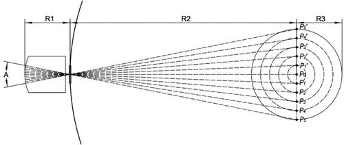
The principle of plasma emission spectroscopy measurement is illustrated as shown in . The spectrometer achieves the acquisition of spectral signals from the plasma radial position points P0, P1, P2, P3, P4, P5, P1’, P2’, P3’, P4’, P5′ by rotating an angle A of the optical fiber probe. The rotating circle center point of the optical fib probe is arranged near an observation window of a microwave resonant cavity. In the diagram, R1 represents the distance from the optical fiber probe head to the observation window while R2 is the distance from the observation window to the center of the plasma within the microwave resonant cavity, and R3 is the radius of the plasma where spectral signals are collected.
Figure 1. The principle of plasma emission spectroscopy measurement.
Chemical vapor deposition of polycrystalline diamond was carried out using single-crystal Si (100) as the substrate, with high-purity H2 (hydrogen) and CH4 (methane) as the gas sources. Using particle size of 0.5–1.5 μm diamond abrasive was mechanically ground on the polished surface of the Si substrate for 15 min, and then the Si substrate treated above is sequentially sonicated in acetone and anhydrous ethanol for 10 min to remove residual surface pollutants. The flow ratio of CH4 to H2 was set at 3/97, and the gas pressure was maintained at 12 kPa, while the microwave power was kept at 10 kW. The growth temperature of the diamond film was controlled within the range of 950 ± 10°C. The experimental parameters for diamond growth were similar to those reported from our previous publications [Citation20]. After the growth process, the silicon substrate was removed by laser cutting and chemical etching to obtain the diamond self-supporting film. Finally, the film was processed using diamond abrasive grinding and polishing methods.
The surface morphology and crystallinity of the diamond films at positions P0, P2, P4 and P5 were analyzed by scanning electron microscopy and Raman spectrometer, respectively. The optical transmittance of the diamond films was measured in the wavelength range of 200–25,000 nm by a UV-visible-near-infrared spectrophotometer with the Agilent Cary 5000 and Fourier-transform infrared spectrometer with the Bruker Invenio S. Room temperature thermal conductivity of the diamond films was tested by a laser flash method with the Netzsch Laser Flash Apparatus LFA 467 [Citation9]. The dielectric constant and dielectric loss of the diamond films at 140 GHz were determined by a quasi-optical resonant cavity technique.
2. Results and discussion
2.1. Plasma emission spectroscopy analysis
The plasma is highly chemically active and contains many of the effective group elements required for the deposition of diamond. The morphological characteristics, the growth rate and the crystal quality of diamond growth are all related to the properties of the plasma. Characterizing macroscopic parameters such as plasma composition, concentration variation, and spatial distribution is the basis for revealing the influence of plasma on deposition results and studying deposition regulation methods [Citation21–23]. Under the experimental conditions of diamond MPCVD, the plasma contains a large number of active hydrogen atoms Hα(α-hydrogen), Hβ(β-hydrogen), Hγ(γ-hydrogen) and carbon-containing groups CH(C–H), C2 (C = C) under H2–CH4 atmosphere. The Hα radical groups state not only play a crucial role in the deposition process of diamond by etching graphite and promoting the formation of the sp3 hybridization of carbon, but also can open C = C bonds and extract active sites of Hα groups in surface C–H [Citation24]. Therefore, higher concentrations of Hα groups have a more pronounced effect on improving diamond quality. The C2 radical groups state was considered as a precursor in the growth process of non-diamond phases. In plasma emission spectroscopy studies, the concentration of C2 groups can be used as a reference for the degree of CH4 dissociation The higher the concentration of C2 groups, the higher the concentration of dissociated methyl groups, indicating a faster diamond growth rate [Citation25]. The concentration of active particles in the plasma is mainly influenced by parameters such as the excitation microwave source power and the gas pressure. The concentration of active particles reflects the degree of dissociation after excitation and is directly proportional to the intensity of the corresponding spectral lines. The spatial distribution of active particles, in addition to the above parameters, depends on the distribution of the microwave field in the microwave resonance cavity of the MPCVD device and the resulting spatial distribution of the plasma.
Therefore, a mixture of 3% methane and 97% hydrogen was used as the excitation source gas for the plasma in this study. Under conditions of 10 kW microwave power and 12 kPa gas pressure, spectral signals were collected using a dual-channel plasma emission spectrometer in the wavelength range of 562–815 nm. The analysis primarily focused on the axial distribution of carbon and hydrogen active particle concentrations to predict the relationship between the effective coverage range of the plasma and the resulting diamond deposition area.
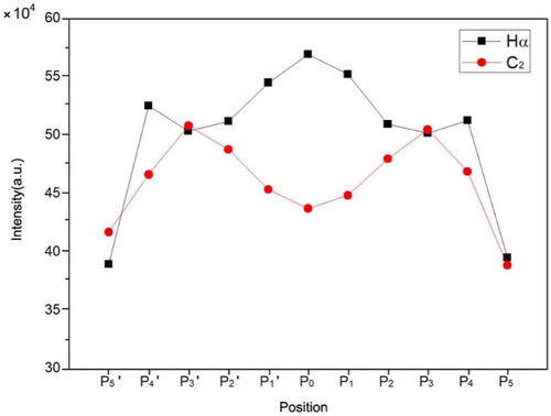
The plasma emission spectroscopy data obtained from full spectrum scanning are shown in . The spectrum primarily exhibits C2 groups at 563, 606, 612, and 619 nm, as well as the Hα spectral line at 656 nm. The intensities of the C2 spectral line at 563 nm and the Hα spectral line at 656 nm were used as parameters for the changes in carbon and hydrogen active particle concentrations. Spectral signals were collected at various radial positions P0, P1, P2, P3, P4, and P5 (at distances of 0.0, 12.5, 25.0, 37.5, 50.0, and 62.5 mm from the plasma center, respectively), as shown in . The changes in the spatial distribution of carbon and hydrogen spectral intensities were characterized by changes in the spatial distribution of carbon and hydrogen reactive particle concentrations. At the positions of P0, P1, P2, and P3, i.e., a plasma diameter of approximately 75 mm, the Hα spectral line intensity is higher at the plasma center and gradually decreases towards the plasma edge. Conversely, the C2 spectral line intensity distribution is the opposite, with lower values at the plasma center and gradually increasing towards the plasma edge. At the P4 position, corresponding to a plasma diameter of approximately 100 mm, there is a small increase and decrease in the intensity of the Hα and C2 spectral lines, respectively. At the P5 position, corresponding to a plasma diameter of approximately 125 mm, both the Hα and C2 spectral line intensities exhibit significant decreases. The spatial distribution changes in Hα and C2 spectral intensities indicate the presence of higher concentrations and chemical reactivity of carbon and hydrogen active particles within a plasma diameter of approximately 100 mm.
Figure 2. The plasma emission spectroscopy of 3% methane and 97% hydrogen.
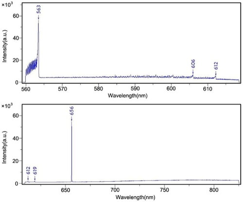
Figure 3. The spectral line intensities of Hα and C2 variation radially across the plasma.
2.2. Growth of diamond film
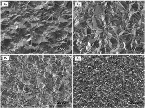
The concentration of hydrogen atoms and carbon-containing groups within the plasma is related to the morphological characteristics, growth rate, and crystal quality of diamond growth [Citation26–28]. The growth of diamond films was carried out under microwave power of 10 kW, air pressure of 12 kPa and growth temperature of 950°C using 3% methane with 97% hydrogen. shows the growth morphology of diamonds at positions P0, P2, P4, and P5. Most diamond at P0, P2, and P4 consists of hexagonal and octahedral grains. Due to the competitive growth between the grains and the growth of more complete large grains interspersed with a small number of incomplete growth of fine grains, the growth of more complete grain size is about 100–200 μm, and incomplete growth of the grain size is 10–50 μm. At the P5 position, the diamond transforms from well-grown large grains to smaller grains with obvious growth defects and a maximum size of 50 μm.
Figure 4. SEM of diamond morphology at positions P0, P2, P4 and P5.
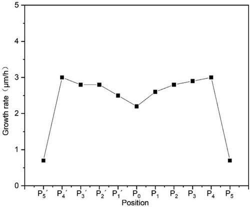
The growth rate of the diamond films varies radially along the plasma, as shown in . The growth rates at positions P0, P2, P4, and P5 are 2.2, 2.8, 3.0, and 0.7 μm/h, respectively. The variations of grain size and growth rate of diamond films are correspond well with the trends of Hα and C2 spectral line intensities along the plasma radius. This is because the grain size and growth rate of diamond films depend on the type and concentration distribution of active particles above the substrate [Citation29–31]. The Hα atoms not only have the function of etching non-diamond phases, but also provide new vacancies for diamond growth, and promote the insertion of carbon groups into the growth layer, thereby facilitating the rapid deposition of high-quality thin films [Citation32]. As the main precursor for diamond growth, the higher the concentration of C2, the higher the concentration of dissociated methyl groups, and the higher the rate of diamond deposition [Citation33,Citation34]. Therefore, the relatively high concentration of Hα and C2 at the P0–P4 position resulted in diamond films with larger grain sizes, intact hexahedral and octahedral crystal patterns, and faster growth rates; the relatively low concentrations of Hα points and C2 at the P5 position resulted in delayed grain growth, smaller grains, and obvious growth defects in the diamond films.
Figure 5. The growth rate of diamond films variation radially along the plasma.
shows the Raman spectra of diamonds at positions P0, P2, P4, and P5. By comparing the peak intensity of the 1332 cm−1 diamond characteristic peak with the half height width (Full Width at Half Maxima FWHM), the maximum value of the peak intensity and the minimum value of the FWHM both appear at the point of P0 position. At position P5, there are significant reductions in peak intensity and broadening of FWHM. This phenomenon can be explained by the trend in carbon and hydrogen spectral line intensities along the plasma radius:
Figure 6. Raman spectra of diamonds at positions P0, P2, P4 and P5.
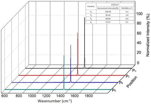
At position P0, the Hα spectral line intensity is higher at the plasma center, while the C2 spectral line intensity is lower at the plasma center. Since hydrogen atoms play an important role in etching the graphite phase and promoting the sp3 hybridization of carbon during the chemical vapor deposition of diamond, a higher concentration of hydrogen atoms and a lower concentration of carbon-containing groups at the P0 position point are conducive to the formation of diamond of higher crystalline quality. Linnik S A et al. studied the vertical distribution of Hα in the H2–CH4 system, and their growth and spectral results showed that the growth rate and mass of diamond decreased with decreasing concentration of H ions, which is similar to the results of the present study [Citation35,Citation36].
At position P5, the intensity of Hα and C2 spectral lines at the P5 position point shows a significant decrease, indicating a significant reduction in the concentration and chemical reactivity of carbon and hydrogen active particles. As a result, the crystallization quality of diamond at the P5 position point is significantly reduced.
Therefore, under the experimental conditions, it is possible to produce diamonds with higher crystal quality at the P0–P4 positions, which corresponds to a diameter of approximately 100 mm.
2.3. Performance test of diamond film
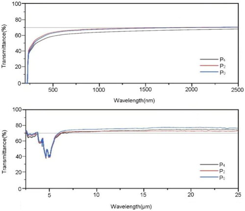
shows the 4-inch (101.6 mm) diameter diamond film prepared at a microwave power of 10 kW. The UV-VIS-NIR transmission spectra of the diamond films measured in the wavelength range from 200 to 25,000 nm after polishing are shown in (the gray horizontal line in the figure represents a transmittance of 70%). Within the tested wavelength range, positions P0, P2, and P4 exhibit consistent optical transmittance. The highest transmittance in the ultraviolet spectrum range (200–400 nm) can reach up to 58%. In the visible spectrum range (400–760 nm), the highest transmittance can reach up to 66%. In the mid-infrared spectral range (2500 ∼ 25,000 nm), the transmittance rate reaches more than 70% except for the intrinsic absorption in the wavelength range of 4000–6000 nm, which is caused by the vibration of diamond double phonons.
Figure 7. Diamond film with diameter of 4 inches.
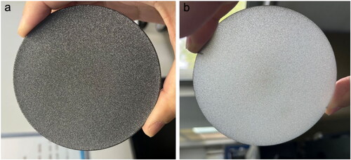
Figure 8. The ultraviolet-visible-near-infrared transmittance spectrum of diamond.
The thermal diffusion coefficient of diamond was measured to be 1035 ± 15 mm2/s by laser flash thermal conductivity meter at room temperature. The thermal conductivity of diamond was calculated to be 1894 W/mK by using the formula λ(T)=a(T)*cp(T)*ρ(T), where: λ=thermal conductivity [W/(m·K)]; a=thermal diffusion coefficient [mm2/s]; cp=specific heat [J/(g·K)], which was taken as the value 0.52 J/(g·K); and ρ=density [g/cm3], which is taken as the value 3.52 g/cm3.
The dielectric properties of diamond were tested using quasi-optical cavity resonator methods at 140 GHz. The measured dielectric constant was 5.48, and the dielectric loss was 5.91 × 10⁻⁵.
3. Conclusion
In this study, the 4-inch diamond self-supported film was prepared using an MPCVD equipment with a microwave frequency of 2.45 GHz at a microwave power of 10 kW. Under the experimental conditions, the plasma emission spectrum primarily consisted of Hα and C2. Within the plasma diameter of about 100 mm, the concentration of carbon and hydrogen reactive particles was higher and the chemical activity was stronger. The results of diamond film growth showed that within this plasma radius of around 100 mm, the growth of polycrystalline diamond grains was uniform and complete, and the crystallization quality of the crystals was high. The prepared diamond self-supporting film has a diameter of 4 inches, with an infrared transmittance exceeding 70%, a thermal conductivity of 1894 W/m·K, a dielectric constant of 5.48, and a dielectric loss of 5.91 × 10⁻⁵.
Author contributions
Shao Junyong: conceptualization, writing—original draft preparation; Cao Bolun: methodology, writing—review and editing; Wu Xiaolei: plasma emission spectroscopy measurement and analysis; Sun Guannan: sample SEM testing analysis; Zhao Jiong: sample preparation and performance testing analysis; Xu Shuai: writing—original draft preparation, Raman testing analysis.
Disclosure statement
No potential conflict of interest was reported by the author(s).
Additional information
Funding
References
- Zhou CG, Qiu R, Ke JL, et al. Research on preparation technology of high quality diamond film. MSF. 2013;749:392–400.
- Qi ZZ, Wei YT, Yu JJ, et al. Surface treatment of an applied novel all-diamond microchannel heat sink for heat transfer performance enhancement. Appl Therm Eng. 2020;177:115489.
- Wang WH, Dai B, Wang Y, et al. Recent progress of diamond optical window-related components. Mater Sci Technol. 2020;28(03):42–57.
- Kumar A, Singh A, Kumar A, et al. Fabrication and characterization of polycrystalline diamond detectors for fast neutron monitoring. Nucl Instrum Methods Phys ResA. 2015;785:55–60.
- Silva F, Achard J, Brinza O, et al. High quality, large surface area, homoepitaxial MPACVD diamond growth. Diamond Relat Mater. 2009;18:683–697.
- Yao K, Dai B, Tan X, et al. Microwave plasma-assisted chemical vapor deposition of microcrystalline diamond films via graphite etching under different hydrogen flow rates. CrystEngComm. 2019;21(15):2502–2507.
- Yan XS. Design and research of 20 kW/915 MHz microwave plasma device. Hefei: university of Science and Technology of China; 2022.
- Gautama P, Toyota H, Iwamoto Y, et al. Synthesizing diamond film on Cu, Fe and Si substrate by in-liquid microwave plasma CVD. Precis Eng. 2017;49:412–420.
- Ding MQ, Li LL, Feng JJ. A study of high-quality freestanding diamond films grown by MPCVD. Appl Surf Sci. 2012;258(16):5987–5991.
- Weng J, Liu F, Xiong LW, et al. Deposition of large areauniform diamond films by microwave plasma CVD. Vacuum. 2018;147:134–142.
- Zhou HY, Xu L, Ogino A, et al. Investigation into the antibacterial property of carbon films. Diamond Relat Mater. 2008;17(7-10):1416–1419.
- Popovich AF, Ralchenko VG, Balla VK, et al. Growth of 4" diameter polycrystailine diamond wafers with high thermal conductivity by 915 MHz microwave plasma chemical vapor deposition. Plasma Sci Technol. 2017;19(3):035503.
- Kobashi K, Nishibayashi Y, Yokota Y, et al. R&D of diamond films in the frontier carbon technology project and related topics. Diamond Relat Mater. 2003;12:233–240.
- Li YF, Tang WZ, Jiang L, et al. Large area high quality diamond films deposition by 915 MHz high power MPCVD reactor. J Synth Cryst. 2019;48(07):1262–1267.
- Li YF, An XM, Liu XC, et al. A 915 MHz/75 kW cylindrical cavity type microwave plasma chemical vapor deposition reactor with a ladder-shaped circumferential antenna developed for growing large area diamond films. Diamond Relat Mater. 2017;78:67–72.
- Weng JW, Xiong LW, Wang JH, et al. Investigation of depositing large area uniform diamond films in multi-mode MPCVD chamber. Diamond Relat Mater. 2012;30:15–19.
- Vikharev AL, Gorbachev AM, Lobaev MA, et al. Multimode cavity type MPACVD reactor for large area diamond film deposition. Diamond Relat Mater. 2018;83:8–14.
- An K, Zhang S, Shao S, et al. Effects of the electric field at the edge of a substrate to deposit a φ100 mm uniform diamond film in a 2.45 GHz MPCVD system. Plasma Sci Technol. 2022;(4):24:1–8.
- Zhang S, An K, Yang Z, et al. 100 mm in diameter diamond films with high uniformity prepared by novel deposition mode in MPCVD system. Vacuum Cryog. 2022;28(05):549–555.
- Xu S, Wu XL, Kang SH. Growth behavior of CVD polycrystalline diamond films on Si, Ti, Mo, Nb, ta substrate surfaces. Superhard Mater Eng. 2020;32(6):1–8.
- Truscott BS, Kelly MW, Potter K J, et al. Microwave plasma-activated chemical vapor deposition of nitrogen-doped diamond. II: CH4/N2/H2 plasmas. J Phys Chem A. 2016;120(43):8537–8549.
- Ma J, Ashfold MNR, Mankelevich YA. Validating optical emission spectroscopy as a diagnostic of microwave activated CH4/Ar/H2 plasmas used for diamond chemical vapor deposition. J Appl Phys. 2009;105(4):1–12.
- Li YC, Hao XB, Dai B, et al. Optimization design of MPCVD single crystal diamond growth based on plasma diagnostics. J Inorg Mater. 2023;38(12):1405–1412.
- Wang CS, Chen HC, Shih WC, et al. Effect of H2/Ar plasma on growth behavior of ultra-nanocrystalline diamond films: the TEM study. Diamond Relat Mater. 2010;19:138–142.
- Huang HW, Zhang TT, Ding KJ, et al. Optical emission spectroscopy analysis of diamond deposited by MPCVD. J Wuhan Instit Technol. 2017;39(1):39–44.
- Lee ST, Lin Z, Jiang X. CVD diamond films: nucleation and growth. Mater Sci Eng. 1999;25:123–154.
- Bushuev EV, Yurov VY, Bolsjakov AP, et al. Express in situ measurement of epitaxial CVD diamond film growth kinetics. Diamond Relat Mater. 2017;72:61–70.
- Jia X, Huang N, Guo Y, et al. Growth behavior of CVD diamond films with enhanced electron field emission properties over a wide range of experimental parameters. J Mater Sci Technol. 2018;34(12):2398–2406.
- Chen GC, Li B, Lan H, et al. Gas phase study and oriented self-standing diamond film fabrication in high power DC arc plasma jet CVD. Diamond Relat Mater. 2007;16:477–480.
- Li B. The influence of DC Arcjet plasma’s properties on deposited diamond. Beijing: University of Science and Technology Beijing; 2014.
- Bolshakov AP, Ralchenko VG, Shu GY, et al. Single crystal diamond growth by MPCVD at subatmospheric pressures. Mater Today Commun. 2017;25:101635.
- Cao W, Ma ZB. Optical spectroscopy for high-pressure microwave plasma chemical vapor deposition of diamond films. Guang Pu Xue Yu Guang Pu Fen Xi. 2015;35(11):3007–3011.
- Ma ZB, Tao LP, Weng GF, et al. Spectroscopic analysis of microwave plasma for chemical vapor deposition diamond. J Wuhan Instit Technol. 2012;34(6):49–52.
- Liao WH, Lin CR, Wei DH. Effect of CH4 concentration on the growth behavior, structure, and transparent properties of ultrananocrystalline diamond films synthesized by focused microwave Ar/CH4/H2 plasma jets. Appl Surf Sci. 2013;270:324–330.
- Linnik SA, Gaydaychuk AV. Application of optical emission spectroscopy for the determination of optimal CVD diamond growth parameters in abnormal glow discharge plasma. Vacuum. 2014;103:28–32.
- Mahoney EJD, Truscott BS, Mushtaq S, et al. Spatially resolved optical emission and modeling studies of microwave-activated hydrogen plasmas operating under conditions relevant for diamond chemical vapor deposition. J Phys Chem A. 2018;122(42):8286–8300.