
Abstract
Diamond has superior physical and electronic properties and it is regarded as an ultimate material of power-electronics applications. Numerous studies have been focusing on the diamond-based power devices, especially on diamond metal-oxide-semiconductor field-effect transistors (MOSFETs). Due to the existence of two-dimensional hole gas (2DHG) layer on the hydrogen-terminated (H-) diamond surface, hole carriers with high density can be provided and thus H-diamond MOSFETs have been widely investigated, whereas they generally exhibit normally on properties. In recent years, many researchers have been devoting themselves to the development of diamond MOSFETs with normally off characteristics and good device performances. In this work, we summarized recent advances to achieve normally off features for diamond MOSFETs, including the partial surface modification or using some specific insulator materials on H-diamond surfaces, the oxidation of the silicon terminated (Si-) diamond, and the inversion-type p-channel diamond MOSFETs on hydroxyl terminated (OH-) diamond. In addition, we summarized their interface properties which mainly limited the device performances, and put forward to the possible approaches to improve the device performances and thus to promote their potential for power application.
1. Introduction
Silicon (Si)-based power devices have been developed and commercialized for a few decades. However, due to the limitation of intrinsic material property of Si, Si power devices cannot meet the demand of power-electronics applications and thus wide bandgap (WBG) semiconductors have been attracting more and more attention. summarized their physical and electronic properties of Si, silicon carbide (SiC), gallium nitride (GaN), gallium oxide (Ga2O3), and diamond [Citation1–5]. Note that further experimental values of the critical fields are needed to make more precise comparison under similar doping levels. Diamond possesses the widest bandgap, the highest breakdown filed, carrier mobility (especially for holes), and thermal conductivity. Therefore, diamond is considered as an ultimate material for high-voltage and high-power applications. Despite outstanding intrinsic properties, the large binding energy between carbon (C) atoms in diamond and its ultra-wide band gap make it difficult to dope or activate doped elements, resulting in low carrier concentration [Citation6–8]. It is worth mentioning that surface transfer doping formed by hydrogen (H-) termination for diamond avoids the doping difficulty and provides a promising way to achieve semiconducting properties for diamond [Citation9–14]. Consequently, numerous researchers have been devoting themselves to the study of diamond-based power devices, particularly of diamond metal-oxide-semiconductor field-effect transistors (MOSFETs). Because of the existence of the two-dimensional hole gas (2DHG) layer formed by surface transfer doping, hydrogen-terminated (H-) diamond MOSFETs basically demonstrate normally on properties, which would cause device failure and would be adverse to practical power applications. Thus, enhancement-mode diamond MOSFETs with normally off characteristics are more competitive, which enables to suppress the static power consumption and save energy [Citation15].
Table 1. Comparison of physical and electronic properties of WBG semiconductors and Si.
Accordingly, H-diamond MOSFETs have been extensively developed worldwide. However, the normally on properties of the H-diamond MOSFETs due to the existence of the 2DHG layer also limit their practical applications. Thus, it is necessary to develop diamond MOSFETs with normally off characteristics. In this work, we introduced current techniques to realize the normally off features and summarized recent processes of the enhancement-mode diamond MOSFETs, including the special surface modification or using some specific insulator materials for H-diamond, developments of other surface terminations of Si- and OH-diamond, and their corresponding device performances. Furthermore, we analyzed the difficulties in each case and put forward to the possible approaches to improve the device performances and thus to facilitate their power application.
2. Recent advances of H-diamond MOSFETs with normally off properties
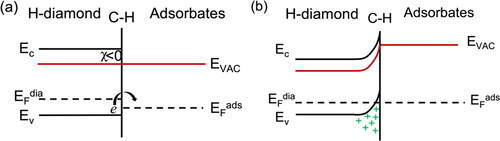
At present, H-diamond MOSFETs have been extensively investigated and Al2O3 formed by atomic layer deposition (ALD) is often employed as the gate oxide [Citation16–22]. Before addressing the techniques and progresses of H-diamond MOSFETs to achieve normally off properties, it is necessary to introduce the history of surface transfer doping and 2DHG formation of H-terminated diamond. Although the formation mechanism of the 2DHG layer is still controversial, most researchers approve of the electric field polarization effect generated by the C-H dipoles on the H-diamond surface [Citation23]. Considering that the electronegativity of C is higher than H [Citation24], a built-in electric field would be formed directing from H to C in the C-H dipole layer on the surface of the H-diamond. Thus, negatively charged adsorbates would be absorbed on the diamond surface. Due to the negative electron affinity (NEA) of H-diamond, the band bending would gradually move upwards with the accumulation of adsorbates [Citation25], resulting in electron escape into the air and the formation of the 2DHG layer on H-diamond surface, as illustrated in , with the hole concentration up to 1013 cm−2 [Citation26]. Thus, the 2DHG layer can provide hole carriers for the source-drain channel of MOSFETs and many researches have made many attempts to increase the hole concentration to the order of 1014 cm−2, such as exposure of the C-H diamond in NO2 ambient or coating specific transition metal oxides on the surface [Citation27,Citation28]. Considering that the existence of the 2DHG layer leads to the normally on properties of H-diamond MOSFETs, which is not competitive for true power applications, some attempts have been made to realize normally off characteristics for H-diamond MOSFETs, which we would like introduce in detail in the following.
Figure 1. Schematic diagrams of energy band bending (a) before and (b) after surface transfer doping on the C-H surface.
2.1. Partial modification of H-termination to achieve normally off properties
Considering that a 2DHG layer is a prerequisite to provide hole carries for the channel of a H-diamond MOSFET, Kawarada’s group has proposed to partially modify the 2DHG layer to break the normally on channel. We have summarized the main techniques to realize normally off characteristics for H-diamond MOSFETs, including the formation of partial O-terminated diamond surface on 2DHG layer, inserting a SiO2 layer, and partial formation of a nitrogen (N)-doped layer. These three methods enable to achieve MOSFETs with normally off characteristics by disrupting the H-diamond surface. shows a cross-sectional schematic diagram of this type of diamond MOSFETs. Furthermore, the relevant manufacturing processes and the electrical properties of MOSFETs were specifically introduced. It should be pointed out that O-terminated diamond possesses a positive electron affinity (PEA), whereas H-terminated one has a NEA as mentioned before. Therefore, Kitabayashi et al. [Citation29] proposed to locally change the 2DHG layer to be the C-O channel, with the purpose of modifying the band diagram and thus controlling the on and off states of the channel.
Figure 2. Schematic cross-section of the H-diamond MOSFETs to achieve normally off properties by partially inserting a C-O channel [Citation29], a SiO2 layer [Citation30], or a N-doped layer [Citation31].
![Figure 2. Schematic cross-section of the H-diamond MOSFETs to achieve normally off properties by partially inserting a C-O channel [Citation29], a SiO2 layer [Citation30], or a N-doped layer [Citation31].](/cms/asset/1f17c007-6347-4867-a9c5-6ba2d9b5a909/tfdi_a_2357654_f0002_c.jpg)
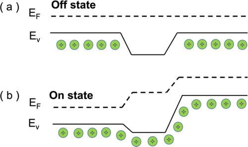
schematically show the band diagrams of the diamond under off and on states, respectively. It is obvious in that the C-O channel enables to form a high energy barrier height due to the PEA and thus to prevent the hole transport in the 2DHG layer when the gate voltage (VGS) is not imposed [Citation32,Citation33]; consequently, the MOSFET is under off state. When a proper negative gate voltage (VGS) is applied, the barrier height gradually decreases and finally, the channel can reach the on state under a certain source and drain voltage (VDS), as illustrated in .
Figure 3. Schematics of band diagrams of diamond under (a) off state (VGS = 0 V) and (b) on state (VGS < 0 V) by inserting a partial C-O channel in the 2DHG layer.
Based on the mechanism analysis, they fabricated a H-diamond MOSFET, accompanied with ultraviolet ozone treatment to form the partial C-O channel with a length of 5 μm. The threshold voltage (Vth) of the MOSFET fluctuated in the range of −4 to −2.5 V, which means they succeeded in developing the H-diamond MOSFETs with normally off characteristics, and the drain off-current density was suppressed in the order of 10−10–10−11 A/mm and the on-off ratio reached 108. It should be noted that not all the MOSFETs with partial C-O channels demonstrate normally off features, which heavily depends on the formation process and coverage rate of the C-O channel. Also, the hole density was significantly reduced and the resultant output current was just −18 mA/mm, much lower than that of the normally on H-diamond MOSFETs [Citation34].
To improve the output performance with guaranteeing normally off properties, Oi et al. [Citation30] put forward to insert a thin SiO2 layer between C-H diamond and Al2O3 to achieve the enhancement-mode MOSFETs. The maximum output current density was increased to 55–140 mA/mm, accompanied with Vth ranging from −6 to −2 V. They measured the square resistance and found that the high-temperature deposition of SiO2 at 450 °C led to the resistance increase, which would be attributed to the desorption of the negatively-charged adsorbates and thus resulted in the reduction of hole density in the 2DHG layer. Besides, the positive oxide charge in SiO2 may compensate for the negative oxide charge in Al2O3, facilitating the normally-off realization.
Based on the concept of partially breaking the 2DHG channel, Kawarada’s group considered to deposit a heavy N-doped layer beneath the 2DHG channel as an alternative to prevent hole accumulation [Citation31,Citation35]. They examined the effects of the N-doping concentration, the length of N-doped layer, and the uniformity on the electrical properties of diamond MOSFETs. The Vth is mainly determined by the doping concentration and uniformity of N. Both would result in Vth fluctuation over a big range; while the length of N-doped layer just slightly affects the Vth according to data statistics. In addition, this technique also faces the similar problem of the low output current density for diamond MOSFETs, and they supposed that it may be attributed to the high density of interface states (Dit). It is indispensable to optimize the doping technique or the ion-implantation technique to improve the device performance.
2.2. Use of other gate insulators instead of Al2O3 to achieve normally off properties
Some researchers have been focusing on employing other gate insulators instead of Al2O3 to achieve normally off properties for H-diamond MOSFETs. shows the schematic of H-diamond MOSFETs, where the gate insulators able to form normally off properties are summarized. Liu et al. have been devoting themselves to investigating the impacts of different high-k gate insulators on device performance of H-diamond MOSFET, especially on the high output current and normally off property [Citation42]. In 2013, they reported the enhancement-mode MOSFET by developing a double-layer HfO2 as the gate insulator [Citation37]. Specifically, a thin HfO2 transition layer (around 4 nm) was first formed by ALD at 120 °C, followed by sputter deposition (SD) to form thick HfO2 (around 30.1 nm). The two-step deposition process is able to protect the H-diamond surface from the plasma discharge during the SD process. The normally off property was realized with Vth of about −1.3 V, and the maxmun output current densiy reached 37.6 mA/mm with a gate length of 4 µm. Then, they proposed to form a logic circuit with combination of the depletion-mode diamond MOSFETs. Besides HfO2, they employed LaAlO3/Al2O3 as the double-layer to fabricate enhancement-mode MOSFETs, with Vth of about −5 V, and manufactured logic circuits by using NOT and NOR logic gate characteristics [Citation38].
Figure 4. Schematic cross-section of using other gate insulators to achieve normally off characteristics for H-diamond MOSFET [Citation36–41].
![Figure 4. Schematic cross-section of using other gate insulators to achieve normally off characteristics for H-diamond MOSFET [Citation36–41].](/cms/asset/9ed3fffa-adc6-4da2-912d-9e07a89f8bd6/tfdi_a_2357654_f0004_c.jpg)
Despite relatively high current density and realization of normally-off charactersistics, the dielectric constant of a double-layer is smaller than that of each single layer [Citation43], which would greatly lower the expectation of device performance. To solve this problem, they performed electron beam evaporation (EB) to form Yttrium oxide (Y2O3) directly on the hydrogen terminal diamond and then prepared the normally off H-diamond MOSFETs [Citation39]. The output current density was dramatically increased to −114.6 mA/mm and the channel mobility was reported to be 35.16 ± 0.5 cm2 V−1s−1. Liu et al. believed that the most likely reason why the device can achieve the normally off characteristics is that the positive charge in the gate insulator compensated the negative charge of the adsorbates on the surface of the H-diamond, and further analyzed the hole transfer mechanism. When a negative gate voltage is applied, the compensation effect of the positive charge in the insulated gate insulator on the negatively charged adsorbent would be weakened. As the gate voltage continues to decrease to the Vth, the hole would accumulate again till forming a p-type conductive channel, as illustrated in .
When considering device power consumption and switching speed, subthreshold swing (SS) is a very important device parameter, and the interface quality plays a crucial role in SS value. Due to the good interfacial properties of stannic oxide (SnO2), Wang et al. [Citation36] deposited SnO2 as a new gate insulator on the hydrogen-terminal diamond surface by EB and obtained a low SS MOSFET. Experiments show that the VTH of the device is −0.12 V and SS is 106.4 mV/dec. SnO2 and other different gate insulators (and structures) can also be used to turn off the conductive channels of the device at VGS equal to zero, which is currently a conventional method for achieving MOSFETs normally off characteristics.
Considering that diamond MESFET has realized the normally off characteristics by employing the metals with low work functions [Citation44], it provides an effective way for H-diamond MOSFETs to achieve normally off properties. Also, it is easy to deposit metals with low work function material and would not cause damage to the diamond surface during the deposition process. Wang et al. have fabricated a series of normally off MOSFETs by using low work function materials. In 2020, they fabricated diamond MOSFETs with a Ti/TiOx double-layer structure [Citation40]. The Vth was −0.14 V when the device gate length was 4 µm, and a maximum mobility of 313 cm2 V−1s−1 when the VGS was −0.2 V. The work function of Ti is lower than that of the H-diamond, so the electrons in Ti enable to flow into the H-diamond side, which would deplete the hole carriers in the 2DHG layer and thus turn off the device. In addition, Wang’s group at Xi’an Jiaotong University has reported a series of insulators that have achieved enhanced diamond MISFETs, such as Lanthanum hexaboride (LaB6) [Citation45], yttrium (Y) [Citation46]. He et al. [Citation47] used Barium fluoride (BaF2) as the gate insulation layer to achieve MISFETs with normally off characteristics. After analyzing the MIS structure, they believe that the normally off characteristic is mainly due to the Schottky barrier depletion effect of gate metal on the channel, followed by charge compensation of positive charges in the gate insulator. However, since the absolute value of Vth (|VTH|) in the reported normally off MOSFETs was generally too small [Citation36,Citation40,Citation45], the device would be turned on accidentally, adverse to the switch application. Therefore, a proper |VTH| is a must to ensure safety and reliability in MOSFET applications [Citation48].
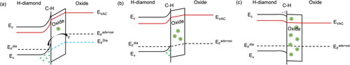
At present, the output capacity of H-diamond MOSFETs is limited by the carrier mobility [Citation49], which is usually between 10 and 100 cm2 V−1s−1 at room-temperature, more than one order of magnitude lower than the intrinsic mobility of bulk diamond (around 3000 cm2 V−1s−1) [Citation50]. In 2020, Sasama et al. [Citation51] proposed to employ hexagonal-boron-nitride (h-BN) as the gate dielectric, and the field-effect mobility of the fabricated diamond FETs achieved 300 cm2 V−1s−1. More importantly, they analyzed the scattering mechanisms, including surface charged impurity scattering, background ionization impurity scattering, acoustic phonon scattering, and surface roughness scattering. They calculated the relationship between carrier density and the mobility of diamond FETs at room-temperature and deduced that the low mobility of H-diamond FETs was caused by surface charged impurity scattering, and reducing surface impurities density can increase carrier mobility. To reduce the density of charged impurities on the H-diamond surface to improve carrier mobility, they fabricated h-BN/diamond FETs in the vacuum environment [Citation41]. They calculated and explained the electrical characteristics, the temperature dependence of electrical properties, the mobility, and normally off operation of h-BN/diamond FETs. The hall mobility evaluated by Hall-effect measurements at room temperature reached 680 cm2 V−1s−1 at VGS of −10 V, which is higher than the performances of other H-diamond MOSFETs and h/BN diamond FETs exposed to air during the fabricating process. The mobility of h-BN/diamond FETs clearly increased with decreasing temperature from 300 to 150 K and the mobility exceeded 1000 cm2 V−1s−1 at 150 K when VGS was −8 V. The hall carrier density versus gate voltage curve at room-temperature indicates the normally off operation of h-BN/diamond FETs with the Vth of −0.99 V. The normally-off operation of the h-BN/diamond FETs was achieved by reducing the negative interface charge, resulting in a negative shift in the threshold voltage. The gate-length-normalized maximum current (LGIDmax/WG) of h-BN/diamond FETs was 1600 μm mA/mm at the gate length of 8.09 μm (the maxmun output current densiy reached 200 mA/mm), which is the highest value reported at present, and the transconductance reached 37 mS/mm. They believe that reducing negatively charged surface impurities would greatly enhance the mobility of charge carriers and overall improve device performance. Note that the key to achieving normally off properties for this kind of H-diamond MOSFETs is the compensation between positive charges in the gate insulator and negative charges on the 2DHG layer. shows the energy band diagram after the deposition of gate insulators and before charge compensation. EFads+oxi stands for the net electron filling level of positive charges in the gate insulator and negative charges on the 2DHG layer, while the blue dashed line represents the electron filling level of H-diamond Fermi level (EFdia) passing through the gate insulator at VGS = 0 V. The positive charges in the gate insulator would offset the negative charges on the 2DHG layer, reducing the hole carrier density and thus resulting in the interruption of the conductive 2DHG channel. However, it should be pointed out that it is difficult to control the amount of positive charges because the charge composition is complex, including the interface traps, border traps, and oxide/insulator raps in the diamond MOS/MIS structures. show the energy band diagrams of gate insulators with different numbers of positive charges after charge compensation. corresponds to a small amount of positive charges in the gate insulator, and thus the conductive channel cannot be turned off completely; corresponds to the band diagram when a large amount of positive charges exits in the gate insulator, and the conductive channel can be turned off. Furthermore, it should be noted that the positive charge density in the gate insulator is uncertain, and the turn-off of the conductive channel is also related to the density of negative charges. Therefore, the characterization and improvement of insulator/diamond interface are significant and need to be studied comprehensively.
Figure 5. Schematics of band diagram changes of (a) after deposition of a gate insulator and before charge compensation, (b) a small amount of positives after charge compensation, and (c) a large amount of positive charges charge after charge compensation.
3. Si-diamond MOSFETs to achieve normally off properties
The particularity of H-diamond surface avoids the doping difficulty and H-diamond MOSFETs have been widely developed and characterized, greatly accelerating diamond power application [Citation52,Citation53]. However, the instability [Citation54] and low carrier mobility [Citation55,Citation56] of H-diamond MOSFETs still limit their application, which forces researchers to explore other terminal modifications and relevant MOSFETs. In 2016, Schenk’s group successfully developed the Si-termination technique on (100) diamond [Citation57] surface for the first time and then they continuously investigated the orientation dependence of diamond, and the Si-(111) diamond [Citation58] structure was also developed. Moreover, Si-diamond shows excellent thermal stability even with thermal oxidation till 1200 °C [Citation59], which is much better than that of H-diamond. Besides, Si-diamond also possesses a NEA [Citation60,Citation61], and thus a p-type channel can be formed due to the surface transfer doping [Citation62,Citation63]. Therefore, the Si-diamond MOSFET is a good alternative for diamond power applications.
In 2020, Kawarada’s group developed the first Si-diamond MOSFETs, where the Si termination was formed by selective growth [Citation64]. Specifically, diamond surface was exposed to ultraviolet radiation in ozone ambient for 3 h to form C-O termination with removal of C-H bonds formed during the MPCVD process. Then, tetraethyl orthosilicate chemical vapor deposition (TEOS-CVD) was applied to deposit a 260 nm-thick SiO2 layer on diamond. Then photolithography and inductively coupled plasma-reactive ion etching (ICP-RIE) were performed to form the strip structure. A boron-doped diamond film was grown with selectively epitaxial growth by MPCVD and C-Si bonds were formed at the SiO2/diamond interface. The MOSFETs were fabricated on the Si-diamond surface with deposition of a Al2O3 passivation layer and formation of source, drain, and gate electrodes [Citation65,Citation66]. The Si-diamond MOSFETs achieved normally off properties with the Vth of around −6 V, and the maximum current density of −165 mA/mm. X-ray photoelectron spectroscopy (XPS) and secondary ion mass spectrometry (SIMS) measurements were performed and the results showed that the Si-terminated diamond structure was composed not by a single Si layer but by multiple Si layers extending from the Si-diamond surface to the inside of SiO2. It is the C-Si bonds that dominate the on- and off-states of the MOSFETs [Citation65]. In addition, the devices showed a good thermal stability, with insuring a high on-off ratio of 106 even at 673 K. However, it should be pointed out that the Si-diamond MOSFETs still face the similar challenge that the Vth fluctuates in a wide range and a fraction of devices demonstrated normally on characteristics. Fu et al. analyzed the surface morphology and element distribution in the SiO2 mark and found that the SiO2 film formed by TEOS-CVD may affect the interface quality and thus degrade the Vth stability. Thus, they removed the SiO2 layer and just used ALD-Al2O3 as the gate oxide of the MOSFETs, and the fluctuation range of Vth was limited within 0.5 V, reduced by 93% [Citation67].
In 2022, Fu et al. [Citation68,Citation69] employed the silicon molecular beam deposition (MBD) technique to form the Si-diamond structure and MOSFETs to achieve the normally off properties. To be specific, a thin Si film with a thickness of 2.7 Å was deposited on the H-diamond surface, followed by vacuum in-situ annealing at 920 °C for 15 min. In this process, the C-H bonds on the H-diamond surface were replaced by the C-Si bonds to form the Si-diamond surface. The gate oxide was Al2O3 deposited by ALD. The Vth of the MOSFET was −10 V, the fluctuation range was 0.2 V, and the maximum leakage current density was −156 mA/mm. In the same year, they developed a SiO2-terminated diamond MOSFET with a source-drain distance (LSD) of 3 μm and the maximum output current density was −311 mA/mm [Citation67], which is the best device performance reported so far among normally off Si-diamond MOSFETs.
Note that the formation of C-Si bonds with high uniformity and high coverage rate is the key to ensuring the superior performance of Si-diamond MOSFETs. During the selective growth process, it is difficult to control the coverage rate of C-Si bonds and the formation and distribution of C-Si-O bonds on the Si-diamond surface. During the preparation of Si-diamond by molecular beam deposition method, Si is easy to be oxidized before deposition, inhibiting the C-Si formation on the diamond surface. It is necessary to optimize the factors that affect the formation of C-Si bonds, such as maintaining the vacuum level of the environment during molecular beam deposition. Furthermore, it is significant to study the atomic substitution and bonding mechanism of diamond surface during the oxidation process to achieve the expected oxidation effect.
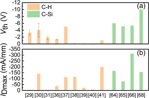
We summarized the reported threshold voltages and the maximum output current density of the enhancement-mode H-diamond and Si-diamond MOSFETs, as illustrated in [Citation29–31,Citation36–41,Citation64–66]. Overall, Si-diamond MOSFETs have both good turnoff capability and output level, while most H-diamond MOSFETs cannot achieve satisfactory device performances in both aspects simultaneously, mainly due to the limitation of H-diamond MOSFETs in achieving normally off characteristics.
Figure 6. Comparison of the reported (a) threshold voltages and (b) maximum output current density for enhancement-mode H-diamond and Si-diamond MOSFETs.
4. OH-diamond MOSFETs to achieve normally off properties
We addressed recent progresses of H- and Si-terminated diamond MOSFETs with normally off characteristics as summarized above. It should be pointed out hole carriers of these devices originate from surface transfer doping. This explains why the normally off yield cannot reach 100% and a fraction of MOSFETs still demonstrate normally on properties despite the identical fabrication process. It is well-known that the traditional inversion-type MOSFETs have been investigated for the other wide bandgap semiconductors, such as SiC because it is feasible for them to realize p-type and n-type doping [Citation70,Citation71]. By overcoming the doping difficulties with researchers at AIST, in 2016, Tokuda’s group developed the first traditional inversion-type p-channel diamond MOSFET [Citation34]. The n-type diamond body was epitaxially grown on a HPHT (111) diamond substrate in prior, followed with selective growth of a p-type epitaxial layer. Note that another key to the inversion-type diamond MOSFET is the formation of hydroxy- (OH-) termination for diamond before depositing ALD-Al2O3, because trimethylaluminium (TMA) is easy to absorb on OH-sites. They formed OH-diamond surface on O-diamond surface followed by water vapor annealing treatment at 500 °C for 1 h. As expected, all of the inversion-type diamond MOSFETs showed normally off properties. The Vth was about −6.3 V. Note that the maximum output current density and hole mobility of the device were respectively 1.6 mA/mm and 8.0 cm2 V−1s−1, which is much lower than the bulk mobility and is far from satisfactory. From their extracted results of subthreshold swing (380 mV/dec), it can be deduced that one main reason for the poor device performance is the high Dit at and near the Al2O3/diamond interface, which is in the order of 1012–1013 cm−2eV−1. Nevertheless, the inversion-type diamond MOSFET is promising in practical applications, owing to its another advantage that the Vth is controllable and can to be modulated by doping concentration of the n-type diamond body layer. They examined the effect of the phosphorous doping concentration (Np) on the device performance. The results showed that the field-effect mobility (μFE) increased with decreasing Np. And μFE reached 20 cm2 V−1s−1 for the MOSFET with NP of 2 × 1015 cm−3 [Citation72].
Except for the OH-diamond formation on O-diamond surface, they also succeeded in forming OH-diamond surface by water vapor annealing on atomically flat H-diamond surface, which was confirmed by Fourier transform infrared (FTIR) spectroscopy with an attenuated total reflectance (ATR) attachment [Citation73]. They studied the impact of annealing temperature on the square resistance of the H-diamond substrate, aiming to examine whether the 2DHG layer was removed or not. The results showed that the square resistance reached 108 Ω/sq when the annealing temperature exceeded 500 °C, indicating the removal of the 2DHG layer. Based on the novel OH-formation technique and the breakthrough of the nitrogen-doping technique, they recently fabricated a new inversion-type diamond MOSFETs and achieved normally off properties. The inversion-type MOSFETs were fabricated on homoepitaxial diamond substrates. In addition, considering the high cost and limited size of the homoepitaxial diamond substrates, Zhang et al. [Citation74] focused on the heteroepitaxial free-standing diamond substrate and fabricated the first inversion-type diamond MOSFETs with normally off characteristics. They compared the Id–Vd and Id–Vg characteristics of inversion-type p-channel MOSFETs fabricated by diamond substrates (with different RMS) grown with homoepitaxy and heteroepitaxy. The main reason for the low mobility of MOSFET is the poor surface and interface quality of the Al2O3/diamond MOS. With regard to the inversion-type diamond MOSFETs, one biggest challenge is the high Dit. They have made comprehensive interface analysis by using diamond MOS capacitors, including the high-low capacitance–voltage (C–V) method at different temperatures, the conductance method, and the simultaneous C–V methods [Citation75,Citation76]. They extracted the energy distribution of Dit and explored the intrinsic properties of the interface states. They also conducted the Kelvin-probe force microscopy (KPFM) measurements for the samples with water vapor annealing treatments and observed the contact potential difference (CPD) between the step-terrace (ST) and bunching-step (BS) regions, which indicated that defects would be formed at steps [Citation77]. They deduced that this would affect the C-OH formation and coverage rate. Nevertheless, further theoretical and experimental investigations are necessary to clarify the physical mechanisms of the interface states. More importantly, it is necessary to explore effective passivation techniques to improve the interface quality of diamond MOS and thus the device performance of inversion-type diamond MOSFETs. In addition, the surface roughness is also a significant parameter for the channel mobility of MOSFETs. Tokuda et al. have developed “lateral overgrowth technique,” which enables to improve the surface morphology greatly. Therefore, it is also important to apply this technique during the fabrication process of MOSFETs, with the purpose of improving the device performance and facilitate the commercialization of diamond electronic applications.
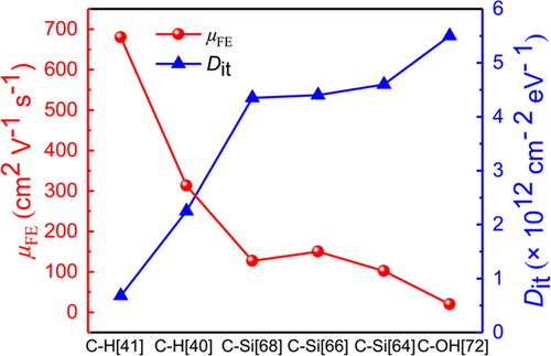
summarizes the reported μFE and Dit for enhancement-mode diamond MOSFETs [Citation40,Citation41,Citation64,Citation66,Citation68,Citation72]. It is obvious that μFE inversely correlates with Dit and the high Dit is one main reason for low μFE of diamond MOSFETs. Therefore, the precise characterization of oxide/diamond interface is significant and passivation techniques are urgent to be developed to reduce the interface and near interface traps in diamond MOS structures.
Figure 7. Summary of the reported μFE and Dit for enhancement-mode diamond MOSFET.
5. Conclusion
Diamond MOSFETs with normally off characteristics are more competitive than those with normally on properties in the field of power electronics applications. In this work, we summarized recent techniques to develop enhancement-mode diamond MOSFETs. Most of the researches have been focusing on the partial modification of H-diamond surface and MOSFETs because of the existence of 2DHG layer. The partial modifications mainly contain the C-O channel formation, N-doped layer formation, employing some particular insulators, double-layer insulator, or specific gate metals with low work function. However, these techniques developed to realize normally off properties for H-diamond MOSFETs are based on introducing defects at and near the diamond MOS/MIS interface, or in the oxide/insulator, including changing the type of dipoles on the substrate surface or introducing fixed positive charges in the gate insulator. Despite the normally off operation, the defect introduction degrades the output capability and Vth stability of the H-diamond MOSFETs. To solve the problems mentioned above to improve the device performances of the enhancement-mode H-diamond MOSFETs, it is necessary to study the mechanism of the atomic substitution of the H-diamond surface and to analyze the energy band structure of the modified diamond surface with other terminations in prior. Based on the mechanism analysis, the termination modification process is needed to be optimized to improve its coverage rate and thus to promote the device performance. In addition, it has been reported that the carrier scattering caused by the interface negative charges would also lead to low carrier mobility [Citation78]. Eliminating interface negative charges would enhance the output capability of diamond MOSFETs with ensuring the normally-off operation. Also, selection of an appropriate gate material is an alternative because the meal work function enables to adjust the Vth without degrading channel mobility.
Except for H-diamond MOSFETs, Si-diamond MOSFETs were also developed to realize the normally-off operation. According to the reported results, Si-diamond MOSFETs showed better device performances with higher output current density compared with those of enhancement-mode H-diamond MOSFETs. The normally-off realization of the Si-diamond MOSFETs was reported to be attributed to the oxidation of C-Si and the resultant formation of C-Si-O bonds. However, the poor coverage rate of C-Si-O bonds would lead to the increase in Dit and decrease in output capacity of the MOSFETs. Therefore, the optimization of C-Si-O formation techniques is important to improve the device performance of the Si-diamond MOSFETs. Besides, the good SiO2/diamond interface and Al2O3/SiO2 interface should be formed by analyzing and controlling the oxidation factors during the SiO2 and Al2O3 deposition process.
In addition, n-type diamond doping techniques by phosphorous and nitrogen have been realized and traditional inversion type p-channel diamond MOSFETs have been developed combined with the technique of OH-diamond formation. This kind of MOSFETs can not only modulate required Vth by adjusting the concentration of impurities in the n-type diamond body but also enable to realize normally-off operation. However, the big issues of the inversion-type diamond MOSFETs are the low channel mobility and output current density, which would be caused by the high density of interface traps, border traps, and oxide traps in diamond MOS structures, and the poor surface morphology of the diamond surface. Therefore, epitaxial techniques accompanied with doping should be developed to improve the quality of diamond surface. Also, the origin of the traps at and near the diamond MOS interface and the oxide traps in the oxide should be clarified, and passivation techniques should be developed to improve the interface quality.
In short, the surface modification of diamond can realize enhancement-mode MOSFETs, which has a big potential in power application fields. To improve the device performance in the next step, it is important to form a better insulator/diamond surface. Specifically, it is indispensable to clarify the reaction mechanism at the atomic level of the termination modification process of diamond, the deposition of gate insulator, as well as the surface properties and atomic structure of diamond after surface reconstruction. Then, the corresponding passivation techniques should be developed to reduce Dit. Meanwhile, the surface morphology of the diamond surface is also needed to be controlled by optimizing the epitaxial techniques to improve the device performances, thus facilitating the power application of the diamond MOSFETs with normally off operation.
Author contributions
Mingkun Li: Methodology, investigation, writing-original draft. Xueqia Zhang: Formal analysis. Shuopei Jiao: Formal analysis. Yanrong Wang: Formal analysis. Shuhua Wei: Formal analysis. Jiang Yan: Formal analysis. Jing Zhang: Formal analysis. Xufang Zhang: Conceptualization, Resources, Supervision, Formal analysis, Writing - review & editing, Funding acquisition, Project administration.
Disclosure statement
No potential conflict of interest was reported by the author(s).
Additional information
Funding
References
- Akimoto I, Handa Y, Fukai K, et al. High carrier mobility in ultrapure diamond measured by time-resolved cyclotron resonance. Appl Phys Lett. 2014;105(3):1.
- Kawarada H. Hydrogen-terminated diamond surfaces and interfaces. Surf Sci Rep. 1996;26(7):205–12.
- Donato N, Rouger N, Pernot J, et al. Diamond power devices: state of the art, modelling, figures of merit and future perspective. J Phys D Appl Phys. 2019;53(9):093001.
- Turner WJ, Fischler AS, Reese WE. Physical properties of several II–V semiconductors. J Phys Rev. 1961;121(3):759–767.
- Higashiwaki M, Kaplar R, Pernot J, et al. Ultrawide bandgap semiconductors. Appl Phys Lett. 2021;118(20):200401.
- Shimaoka T, Liao M, Koizumi S. n-Type diamond metal-semiconductor field-effect transistor with high operation temperature of 300 °C. IEEE Electron Device Lett. 2022;43(4):588–591.
- Childress L, Hanson R. Diamond NV centers for quantum computing and quantum networks. MRS Bull. 2013;38(2):134–138.
- Lagrange J-P, Deneuville A, Gheeraert E. Activation energy in low compensated homoepitaxial boron-doped diamond films. Diamond Relat Mater. 1998;7(9):1390–1393.
- Imanishi S, Horikawa K, Oi N, et al. 3.8 W/mm RF power density for ALD Al2O3-based two-dimensional hole gas diamond MOSFET operating at saturation velocity. IEEE Electron Device Lett. 2019;40(2):279–282.
- Yu X, Zhou J, Qi C, et al. A high frequency hydrogen-terminated diamond MISFET with fT/fmax of 70/80 GHz. IEEE Electron Device Lett. 2018;39(9):1373–1376.
- Yu C, Zhou C, Guo J, et al. Hydrogen-terminated diamond MOSFETs on (001) single crystal diamond with state of the art high RF power density. Funct Diamond. 2022;2(1):64–70.
- Kudara K, Imanishi S, Hiraiwa A, et al. High output power density of 2DHG diamond MOSFETs with thick ALD-Al2O3. IEEE Trans Electron Devices. 2021;68(8):3942–3949.
- Zhou CJ, Wang JJ, Guo JC, et al. Radiofrequency performance of hydrogenated diamond MOSFETs with alumina. Appl Phys Lett. 2019;114(6):063501.
- Liu JW, Liao MY, Imura M, et al. Control of normally on/off characteristics in hydrogenated diamond metal-insulator-semiconductor field-effect transistors. J Appl Phys. 2015;118(11):115704.
- Zhu X, Shao S, Chan S, et al. High performance of normally‐on and normally‐off devices with highly boron‐doped source and drain on H‐terminated polycrystalline diamond. Adv Elect Mater. 2023;9(3):2201122.
- Kazuyuki H, Hidenori T, Shintaro Y, et al. High-performance p-channel diamond MOSFETs with alumina gate insulator. 2007 IEEE International Electron Devices Metting; 2007. p. 873–876.
- Kasu M, Sato H, Hirama K. Thermal stabilization of hole channel on H-terminated diamond surface by using atomic-layer-deposited Al2O3 overlayer and its electric properties. Appl Phys Express. 2012;5(2):025701.
- Kawarada H. High-current metal oxide semiconductor field-effect transistors on H-terminated diamond surfaces and their high-frequency operation. Jpn J Appl Phys. 2012;51(9R):090111.
- Yu C, Zhou C, Guo J, et al. RF performance of hydrogenated single crystal diamond MOSFETs. 2019 IEEE International Conference on Electron Devices and Solid-State Circuits (EDSSC); 2019.
- Ren Z, Lv D, Xu J, et al. High temperature (300 °C) ALD grown Al2O3 on hydrogen terminated diamond: band offset and electrical properties of the MOSFETs. Appl Phys Lett. 2020;116(1):013503.
- Wang Y-F, Wang W, Abbasi HN, et al. LiF/Al2O3 as dielectrics for MOSFET on single crystal hydrogen-terminated diamond. IEEE Electron Device Lett. 2020;41(6):808–811.
- Hirama K, Sato H, Harada Y, et al. Diamond field-effect transistors with 1.3 a/mm drain current density by Al2O3 passivation layer. Jpn J Appl Phys. 2012;51(9R):090112.
- Kawarada H. Diamond p-FETs using two-dimensional hole gas for high frequency and high voltage complementary circuits. J Phys D Appl Phys. 2023;56(5):053001.
- Kawai S, Yamano H, Sonoda T, et al. Nitrogen-terminated diamond surface for nanoscale NMR by shallow nitrogen-vacancy centers. J Phys Chem C. 2019;123(6):3594–3604.
- Nebel CE, Ertl F, Sauerer C, et al. Low temperature properties of the p-type surface conductivity of diamond. Diamond Relat Mater. 2002;11(3–6):351–354.
- Oing D, Geller M, Lorke A, et al. Tunable carrier density and high mobility of two-dimensional hole gases on diamond: the role of oxygen adsorption and surface roughness. Diamond Relat Mater. 2019;97:107450.
- Sato H, Kasu M. Maximum hole concentration for hydrogen-terminated diamond surfaces with various surface orientations obtained by exposure to highly concentrated NO2. Diamond Relat Mater. 2013;31:47–49.
- Tordjman M, Weinfeld K, Kalish R. Boosting surface charge-transfer doping efficiency and robustness of diamond with WO3 and ReO3. Appl Phys Lett. 2017;111(11):111601.
- Kitabayashi Y, Kudo T, Tsuboi H, et al. Normally-off C–H diamond MOSFETs with partial C–O channel achieving 2-kV breakdown voltage. IEEE Electron Device Lett. 2017;38(3):363–366.
- Oi N, Yabe T, Jorge SO, et al. Normally-off 2DHG diamond Al2O3/SiO2 MOSFETs without deteriorating drain current density. Extended Abstracts of the 2018 International Conference on Solid State Devices and Materials; 2018. p. 265–266.
- Oi N, Kudo T, Inaba M, et al. Normally-off two-dimensional hole gas diamond MOSFETs through nitrogen-ion implantation. IEEE Electron Device Lett. 2019;40(6):933–936.
- Grivickas P, Ščajev P, Kazuchits N, et al. Carrier recombination parameters in diamond after surface boron implantation and annealing. J Appl Phys. 2020;127(24):245707.
- Itoh Y, Sumikawa Y, Umezawa H, et al. Trapping mechanism on oxygen-terminated diamond surfaces. Appl Phys Lett. 2006;89(20):203503.
- Matsumoto T, Kato H, Oyama K, et al. Inversion channel diamond metal-oxide-semiconductor field-effect transistor with normally off characteristics. Sci Rep. 2016;6(1):31585.
- Oi N, Inaba M, Okubo S, et al. Vertical-type two-dimensional hole gas diamond metal oxide semiconductor field-effect transistors. Sci Rep. 2018;8(1):10660.
- He S, Wang W, Chen G, et al. Small subthreshold swing diamond field effect transistors with SnO2 gate dielectric. IEEE Trans Electron Devices. 2022;69(8):4427–4431.
- Liu JW, Liao MY, Imura M, et al. Normally-off HfO2-gated diamond field effect transistors. Appl Phys Lett. 2013;103(9):092905.
- Liu J, Ohsato H, Liao M, et al. Logic circuits with hydrogenated diamond field-effect transistors. IEEE Electron Device Lett. 2017;38(7):922–925.
- Liu JW, Oosato H, Liao MY, et al. Enhancement-mode hydrogenated diamond metal-oxide-semiconductor field-effect transistors with Y2O3 oxide insulator grown by electron beam evaporator. Appl Phys Lett. 2017;110(20):203502.
- Zhang M, Wang W, Chen G, et al. Normally off hydrogen-terminated diamond field-effect transistor with Ti/TiOx gate materials. IEEE Trans Electron Devices. 2020;67(11):4784–4788.
- Sasama Y, Taisuke K, Masataka I, et al. High-mobility p-channel wide bandgap transistors based on h-BN/diamond heterostructures. arxiv Preprint. 2021;2102,05982.
- Cheng S, Sang L, Liao M, et al. Integration of high-dielectric constant Ta2O5 oxides on diamond for power devices. Appl Phys Lett. 2012;101(23):232907.
- Liu J, Liao M, Imura M, et al. Low on-resistance diamond field effect transistor with high-k ZrO2 as dielectric. Sci Rep. 2014;4(1):6395.
- Liao M, Sang L, Shimaoka T, et al. Energy‐efficient metal–insulator–metal‐semiconductor field‐effect transistors based on 2D carrier gases. Adv Elect Mater. 2019;5(5):1088832.
- Wang W, Wang Y, Zhang M, et al. An enhancement-mode hydrogen-terminated diamond field-effect transistor with lanthanum hexaboride gate material. IEEE Electron Device Lett. 2020;41(4):585–588.
- Zhang M, Wang W, Chen G, et al. Electrical properties of yttrium gate hydrogen-terminated diamond field effect transistor with Al2O3 dielectric layer. Appl Phys Lett. 2021;118(5):053506.
- He Q, Su K, Zhang J, et al. High mobility normally-off hydrogenated diamond field effect transistors with BaF2 gate insulator formed by electron beam evaporator. IEEE Trans Electron Devices. 2022;69(3):1206–1210.
- Hua M, Chen J, Wang C, et al. E-mode p-GaN gate HEMT with p-FET bridge for higher VTH and enhanced VTH stability. 2020 IEEE International Electron Devices Meeting (IEDM); 2020.
- Verona C, Arciprete F, Foffi M, et al. Influence of surface crystal-orientation on transfer doping of V2O5/H-terminated diamond. Appl Phys Lett. 2018;112(18):181602.
- Daligou G, Pernot J. 2D hole gas mobility at diamond/insulator interface. Appl Phys Lett. 2020;116(16):162105.
- Sasama Y, Taisuke K, Katsuyoshi K, et al. Charge-carrier mobility in hydrogen-terminated diamond field-effect transistors. J Appl Phys. 2020;127(18):185707.
- Cui A, Zhang J, Ren Z, et al. Microwave power performance analysis of hydrogen terminated diamond MOSFET. Diamond Relat Mater. 2021;118:108538.
- Saha NC, Kim S-W, Oishi T, et al. 345-MW/cm2 2608-V NO2 p-type doped diamond MOSFETs with an Al2O3 passivation overlayer on heteroepitaxial diamond. IEEE Electron Device Lett. 2021;42(6):903–906.
- Chen Z, Yu X, Zhou J, et al. Negative constant voltage stress-induced threshold voltage instability in hydrogen-terminated diamond MOSFETs with low-temperature deposited Al2O3. Appl Phys Lett. 2020;117(13):133501.
- Hayashi K, Yamanaka S, Okushi H, et al. Study of the effect of hydrogen on transport properties in chemical vapor deposited diamond films by hall measurements. Appl Phys Lett. 1996;68(3):376–378.
- Geis MW, Hollis MA, Turner GW, et al. Controlling the carrier density of surface conductive diamond. Diamond Relat Mater. 2022;122:108775.
- Schenk A, Tadich A, Sear M, et al. Formation of a silicon terminated (100) diamond surface. Appl Phys Lett. 2015;106(19):191603.
- Schenk AK, Sear MJ, Dontschuk N, et al. Development of a silicon–diamond interface on (111) diamond. Appl Phys Lett. 2020;116(7):071602.
- Sear MJ, Schenk AK, Tadich A, et al. Thermal stability and oxidation of group IV terminated (100) diamond surfaces. Phys Status Solidi A. 2018;215(22):1800283.
- Schenk AK, Tadich A, Sear MJ, et al. The surface electronic structure of silicon terminated (100) diamond. Nanotechnology. 2016;27(27):275201.
- Zhu X, Bi T, Yuan X, et al. C-Si interface on SiO2/(111) diamond p-MOSFETs with high mobility and excellent normally-off operation. Appl Surf Sci. 2022;593:153368.
- Oslinker B, Hoxley D, Tadich A, et al. Surface transfer doping of oxidised silicon-terminated (111) diamond using MoO3. Diamond Relat Mater. 2023;133:109712.
- Sear MJ, Schenk AK, Tadich A, et al. P-type surface transfer doping of oxidised silicon terminated (100) diamond. Appl Phys Lett. 2017;110(1):011605.
- Fei W, Bi T, Iwataki M, et al. Oxidized Si terminated diamond and its MOSFET operation with SiO2 gate insulator. Appl Phys Lett. 2020;116(21):212103.
- Bi T, Chang Y, Fei W, et al. C–Si bonded two-dimensional hole gas diamond MOSFET with normally-off operation and wide temperature range stability. Carbon. 2021;175:525–533.
- Fu Y, Chang Y, Zhu X, et al. 300 mA/mm drain current density P-type enhancement-mode oxidized Si-terminated (111) diamond MOSFETs with ALD Al2O3Gate insulator. 2022 IEEE 34th International Symposium on Power Semiconductor Devices and ICs (ISPSD); 2022.
- Fu Y, Chang Y, Zhu X, et al. Normally-off oxidized Si-terminated (111) diamond MOSFETs via ALD-Al2O3 gate insulator with drain current density over 300 mA/mm. IEEE Trans Electron Devices. 2022;69(8):4144–4152.
- Fu Y, Chang Y, Kono S, et al. −10 V threshold voltage high-performance normally-off C–Si diamond MOSFET formed by p+-diamond-first and silicon molecular beam deposition approaches. IEEE Trans Electron Devices. 2022;69(5):2236–2242.
- Fu Y, Kono S, Kawarada H, et al. Electrical characterization of metal/Al2O3/SiO2/Oxidized-Si-terminated (C–Si–O) diamond capacitors. IEEE Trans Electron Devices. 2022;69(7):3604–3610.
- Roccaforte F, Fiorenza P, Vivona M, et al. Selective doping in silicon carbide power devices. Materials. 2021;14(14):3923.
- Zheng Z, Zhang L, Song W, et al. Threshold voltage instability of enhancement-mode GaN buried p-channel MOSFETs. IEEE Electron Device Lett. 2021;42(11):1584–1587.
- Zhang X, Matsumoto T, Yamasaki S, et al. Inversion-type p-channel diamond MOSFET issues. J Mater Res. 2021;36(23):4688–4702.
- Yoshida R, Miyata D, Makino T, et al. Formation of atomically flat hydroxyl-terminated diamond (1 1 1) surfaces via water vapor annealing. Appl Surf Sci. 2018;458:222–225.
- Zhang X, Matsumoto T, Nakano Y, et al. Inversion channel MOSFET on heteroepitaxially grown free-standing diamond. Carbon. 2021;175:615–619.
- Zhang X, Matsumoto T, Sakurai U, et al. Energy distribution of Al2O3/diamond interface states characterized by high temperature capacitance-voltage method. Carbon. 2020;168:659–664.
- Zhang X, Matsumoto T, Sakurai U, et al. Insight into Al2O3/B-doped diamond interface states with high-temperature conductance method. Appl Phys Lett. 2020;117(9):092104.
- Nagai M, Yoshida R, Yamada T, et al. Conductive-probe atomic force microscopy and kelvin-probe force microscopy characterization of OH-terminated diamond (111) surfaces with step-terrace structures. Jpn J Appl Phys. 2019;58(SI):SIIB08.
- Pernot J, Volpe PN, Omnès F, et al. Hall hole mobility in boron-doped homoepitaxial diamond. Phys Rev B. 2010;81(20):205203.