Abstract
Bi2 Sr2 CaCu2 Ox/AgMg conductors are potentially important for many applications up to 20 K, including magnets for cryogen-free magnetic resonance imaging and high field nuclear magnetic resonance research. One promising approach to increased critical current density is partial-melt processing in the presence of a magnetic field which has been shown to enhance c-axis texturing of wide, thin tape conductors. Here, we report on low aspect ratio rectangular conductors processed in an 8 T magnetic field. The magnetic field is applied during different stages of the heat treatment process. The conductors are electrically characterized using four-point critical current measurements as a function of magnetic field and magnetic field orientation relative to the conductor. The superconductive transition and magnetization hysteresis are measured using a SQUID magnetometer. The microstructures are characterized using scanning electron microscopy and energy dispersive spectroscopy and analyzed using digital image processing. It is found that the presence of a magnetic field during split melt processing enhances the electrical transport and magnetic behavior, but that the anisotropy is not consistently affected. The magnetic field also affects development of interfilamentary Bi2212 bridges, and that this depends on the initial shape of the Bi2212 filament. At least two behaviors are identified; one impacts the oxide phase assemblage and the other impacts textured growth.
Introduction
The development of cryogen free superconducting magnets has contributed significantly to an expanding role of magnetic fields in materials synthesis and processing and magnetic field has been recognized not only as a parameter for studying physical properties but also as a tool to control microstructure and properties [Citation1, Citation2]. Owing to the magnetic anisotropy of certain crystal structures, grain alignment and crystal orientation by the application of a magnetic field has led to interesting phenomena. The experimental research has demonstrated that magnetic field can have a significant effect on the solidification [Citation3–5], solid phase transformations [Citation6, Citation7], grain growth and grain boundary motion [Citation8], electro-deposition [Citation9], vapor-deposition [Citation10], alignment of CNT in composites and neat macroscopic membranes [Citation11].
Of the numerous high temperature superconductors (HTS) discovered since 1987, Bi2 Sr2 CaCu2 Ox /AgMg (Bi2212/AgMg) composites are the only ones made in the form of a round cross-section wire with high critical current density (Jc), high engineering critical current density (Je) and no anisotropy. Based on performance, available length and potential for further improvement, it is a likely material to enable superconducting magnets generating above 25 T [Citation12]. For a number of years, Bi2212 research and development focused on very wide, thin, tape conductors, with aspect ratios on the order of 20 or higher and relatively low filament counts [Citation13–19]. These conductors are highly anisotropic with respect to their electromagnetic properties, and geometrically well suited for magnetic field processing. Recently, however, the focus for Bi2212 R&D has shifted to round wire and low aspect ratio (1–2) geometries [Citation20, Citation21]. For reasons not yet fully understood, these conductors now show isotropic electromagnetic behavior and higher Je than the wide tape conductors. From the perspective of magnet construction, they are preferable because they are likely to result in significantly higher fill-factor than wide, thin tape conductors [Citation22].
Powder-in-tube manufacturing and partial-melt processing are typically used techniques for producing Bi2212 tapes and wires [Citation23]. Powder-in-tube manufacturing is a batch process whereby the starting oxide powder is packed within a pure Ag tube and mechanically drawn into wire via traditional wire drawing technology. Typically, the outermost sheathing is a Ag-alloy, such as AgMg. Partial melt-processing consists of melting the material above its peritectic temperature, slow cooling to a temperature below T solidus, and subsequently sintering within the Bi2212 solid state. Note that because this heat treatment has a peak temperature above the peritectic temperature, the starting powder melts incongruently, forming several non-superconducting crystalline phases within a liquid phase, resulting in densification but also some phase segregation. When this is cooled properly, well-connected, well-aligned Bi2212 grains form from reactions between the liquid and the crystalline phases present in the partial-melt. During subsequent solid-state growth, Bi2212 grain alignment can result while the size of non-superconducting grains is reduced.
Due to the highly anisotropic crystal structure and electromagnetic behavior of HTS materials, the transport Jc is strongly dependent on grain alignment and long-range texture is typically an important aspect of conductor processing. Several texturing techniques have been successfully used on Y-Ba-Cu-O and Bi-Sr-Ca-Cu-O superconductors, including solidification in a thermal gradient [Citation24–26], in a high magnetic field [Citation18, Citation27–30], floating zone [Citation31, Citation32], composite reaction texturing processes [Citation33], and templated growth on a textured substrate [Citation34–37]. Among the different techniques for producing grain alignment, processing in an external magnetic field is a demonstrated technique that also improves Jc HTS materials. Many efforts have been carried out for texture development in Bi2212 bulks and thick films or tapes by magnetic melt processing (MMP), during which the partial melt and solidification steps of the Bi2212 heat treatment are performed within a large magnet. It was demonstrated that a uniformly high degree of texture with the c-axis parallel to the direction of magnetic field applied during MMP is formed throughout the thickness of monocore tapes and bulk samples [Citation28, Citation38]. Misalignment angles are reduced in multifilamentary Bi2212 tapes textured in a magnetic field [Citation29]. The underlying mechanisms for obtaining improved texture and properties by magnetic field processing of Bi2212 remain uncertain. One possibility is related to the existence of anisotropy in the paramagnetic susceptibility. The source of such anisotropy, however, is unclear, particularly considering that the processing involves peritectic melting. It is also unknown if magnetic field processing affects Bi2212 processing through mechanisms other than texturing. For example, it is unknown if the presence of magnetic field alters the phase assemblage or the phase diagram.
Traditionally there are two approaches for manufacturing superconducting magnets. The react&wind (R&W) approach is typically used for NbTi magnets while the wind&react (W&R) approach was developed for Nb3 Sn due to its intrinsic strain sensitivity. For Bi2212, both methods have been used [Citation14, Citation16] but each has fundamental limitations. To improve upon Bi2212 magnet manufacturing, a new approach has recently been developed, react-wind-sinter (RWS), to avoid the primary issues that limit W&R and R&W manufacturing. For this manufacturing approach, a two-step process (`split melt processing') is used. Initial results show that this approach has significant benefits and further development is on-going [Citation39–41]. One of the primary differences between SMP and conventional processing is that the Bi2212 undergoes two heat treatments. In the first, the Bi2212 is partially melted and solidified. It is then cooled to room temperature (at which point a magnet can be wound) and then reheated for subsequent solid-state sintering. This is illustrated in figure .
Figure 1 Split melt process used for the magnetic field processing experiments. The four processes, A, B, C and D refer to the various permutations of using magnetic field as illustrated.
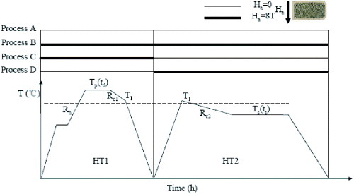
Here we report on investigations on split melt-processing of Bi2212/AgMg low aspect ratio multifilamentary wires using an 8 T magnetic field. Experiments are performed including the four permutations of magnetic field `on' and `off' during SMP as illustrated in figure . After heat treatment, the electromagnetic properties of the wires are characterized, including the dependence of the transport critical current (Ic) on magnetic field and magnetic field angle, superconducting transition temperature, and magnetization hysteresis, in order to determine the effects of magnetic field during different stages of the heat treatment process. These measurements are used to quantify the anisotropy in terms of electrical and magnetic behavior. Microstructures were examined using scanning electron microscopy (SEM) and image analysis is used to begin understanding if magnetic fields alter the phase assemblage.
Experimental approach
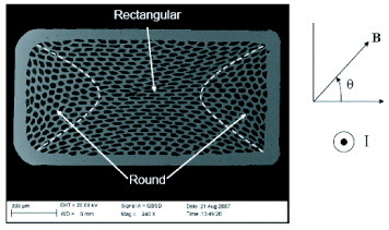
Single restack powder-in-tube Bi2212/AgMg rectangular wire with an aspect ratio equal to two is provided by Supercon, Inc. [Citation42]. The wire consists of 502 filaments with cross-sectional dimensions of 1.2 × 0.6 mm2 and is shown in figure in the as-drawn state (i.e. before heat treatment). Note that there are two distinct regions within the wire, separated by an hour-glass shape, as illustrated on the image in figure . In the outer portions, the filaments remain round and are ∼ 25 μ m in diameter, while in the center, top and bottom, the filaments are elongated and ∼ 45 μm× 10 μ m, which is a larger aspect ratio than that of the wire itself.
Figure 2 Cross-section of the rectangular wire before heat treatment. The curves drawn on the image roughly separate the regions of round filaments from regions of aspect filaments. The scale bar shown equals 200 μ m. The neighboring diagram illustrates the definition of the angle θ, which is the angle between wide plane and the magnetic field applied during measurements.
For each heat treatment run, 12 samples, each 45 mm long, are cut from one batch of wire, placed in a ceramic sample holder and introduced into a vertical furnace within a superconducting magnet. During all heat treatments, the magnet either provides an 8 T magnetic field parallel to the long axis of the furnace or it is off. The experimental setup was described in detail previously [Citation29]. A version of the split melt process, consisting of a reaction step and a sintering step, is employed as illustrated in figure . Details of the temperatures, times and ramp rates, corresponding to the heat treatment in figure , are given in table . Also shown in figure is the direction of magnetic field during heat treatment, which is not varied in these experiments. For the runs with the magnetic field on, the field is first increased to 8 T and the furnace temperature subsequently increased to the desired value. After heat treatment, the temperature is decreased to room temperature and only then is the magnetic field returned to zero. All heat treatments are performed in flowing oxygen. Note that, before processing, the furnace is profiled to obtain the temperature distribution within the furnace at the peak processing temperature. The sample holder is such that, for each run, the 12 samples result in six sets of two samples that have seen the same peak temperature. All 12 samples are measured and the pair with the highest performance for each magnetic-field process (A, B, C and D in figure ) are studied in detail and reported here. This overcomes any potential run-to-run variation within the furnace that may otherwise influence the interpretation of the effects of magnetic field processing.
Table 1 Heat treatment parameters corresponding to figure .
All Ic measurements are at 4.2 K in a liquid helium bath using the four-point method and a 1 V cm- 1 electric field criterion. Transport measurements are made using a probe with a rotating sample holder to allow for measurement at varying field angles from 0 to 90° in magnetic fields up to 5 T. This is discussed in detail in [Citation29, Citation30]. The definition of the magnetic field angle during measurement, θ, is illustrated in figure . Note that the applied magnetic field is perpendicular to the transport current for all magnetic field orientations, and that θ = 90° corresponds to the magnetic field during measurement being parallel to the magnetic field during processing. To avoid Lorentz-force induced damage to the conductor during in-field measurements, the samples are glued to a G-10 plate which provides structural support to the sample. The G-10-reinforced sample is then mounted on the measurement probe. Magnetization properties are measured using a Quantum Design superconducting quantum interference device (SQUID) magnetometer. For critical temperature (Tc) measurements, the field was first set at 100 G and held constant throughout the measurement. Magnetization hysteresis in magnetic fields up to 5 T is measured in the temperature range of 4.2–40 K. The same definition of θ applies to magnetization measurements as to transport measurements. Polished transverse cross-sectional microstructures were observed by SEM and energy dispersive spectroscopy (EDS) on a Zeiss 1540 XB microscope. Back-scattered electron images are used to produce contrast from the different phases consisting of different elements. Images were analyzed quantitatively using ImageJ. Each of the primary phases present (Ag, Bi2212, alkaline earth cuprates (AEC) and Bi2201) is recognized by its grayness range (using 8-bit grayscale) as indicated in table . To estimate the amount of Bi2212 phase present in the microstructure, the Ag area is first removed from the image and the area fractions of the remaining oxide phases are then calculated by the `measure' tool within the ImageJ software. Although it is difficult at times to differentiate between all of the non-Bi2212 phases, the Bi2212 phase identification is distinct (and supported by EDS), so results are reported in terms of the percentage of Bi2212 in the non-Ag area.
Table 2 Grayness ranges used for phase identification in ImageJ.
Results
Magnetic field and angular dependence of critical current and average grain alignment
Figure shows Je (θ = 0) at 4.2 K in self-field and at 5 T for all four sample types. Illustrated values are the average of two samples of each type. Note that Je is reported, defined as Ic divided by the wire cross-sectional area, rather than Jc, which would require an accurate measurement of the Bi2212 filament cross-sectional area. Since all samples originate from the same batch of wire, this provides a comparison between samples without attempting to determine the filament fraction after deformation and processing. With the application of magnetic field during both heat treatments (process B) or only during the partial-melt and resolidification but not the subsequent sintering (process C), Je increases relative to the other processes by a small but significant amount (8.9–9.7%). The presence of magnetic field only during sintering (process D) has no impact on the transport behavior. Figure shows the dependence of the normalized Ic on the magnetic field angle for all four sample types. A strong dependence exists for all samples. With the application of magnetic field during split melt processing, however, the field angle dependence on Ic is increased, especially for the wire with the magnetic field applied during both heat treatments (process B) as compared to those without magnetic field.
Figure 3 Je (4.2 K) in self-field and at 5 T, θ = 0°, for the four sample types. Values are provided atop each bar in A min- 2.
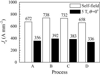
Figure 4 Dependence of Ic (4.2 K) on magnetic field angle at 5 T for all four sample types. The angle dependence is seen by plotting the critical current normalized to its peak value.
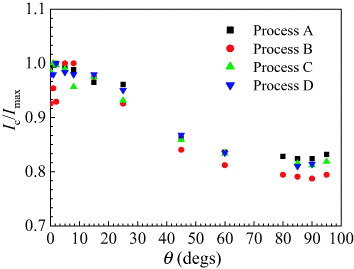
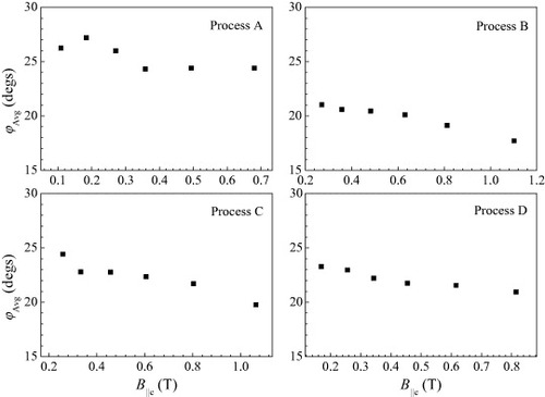
Figure shows the average misalignment angle, ϕ avg, of samples treated with and without magnetic field as calculated using (1) and following the approach detailed in [Citation30, Citation43]:
1 In this formulation, which is derived in [Citation30], Ba and Bb are defined such that Ic (Ba ,θ = 0) =Ic (Bb ,θ = 90° ), where θ is the angle between the magnetic field and the plane of the tape as illustrated in figure . ϕ avg range from 24.3° to 27.2° for process A, 17.7° to 21.0° for process B, 19.8°to 24.4° for process C and 20.9° to 23.3° for process D. ϕ avg is related to a combination of the crystallographic grain misalignment within the wires and the impact of grain misalignment on intergranular transport. With the application of magnetic field during treatment, ϕ avg decreases indicating improved grain alignment. Note that ϕ avg = ϕ avg (B), and that in all cases ϕ avg decreases for increasing B. This is due to the fact that the grain misalignment angle, as determined by in-field electrical transport measurements, represents a combination of the crystallographic grain alignment and the intergranular coupling of the grains carrying the transport current. Intergranular coupling between grains can be modeled as a combination of `weakly linked' current paths and `strongly linked' current paths [Citation44, Citation45]. As the magnetic field increases, the weakly linked current paths no longer support transport current, so the measurement becomes indicative of the strongly linked paths, which have less grain misalignment. Thus, at higher field, the grain misalignment angle, as defined by equation (Equation1
1 ), decreases, because only the better aligned grains are carrying transport current.
Figure 5 The average grain misalignment angle of samples of all four sample types.
Superconductive transition and magnetization hysteresis
Figure shows the superconducting transitions measured magnetically in a SQUID magnetometer with a 100 G background magnetic field with θ = 0 and 90°. The diamagnetic susceptibilities for θ = 0° are lower than those for θ = 90° for all sample types. With the application of high magnetic field during processing, regardless of which stage of the process, the diamagnetic moment and the sharpness of the transition increase relative the process A samples, regardless of the magnetic field orientation during measurement. The difference, however, is significantly greater for θ = 0°. These results indicate that the presence of magnetic field during processing impacts not only the crystallographic texture, but also grain-to-grain coupling and the volume fraction of Bi2212 phase formed within the oxide filaments [Citation46]. There are also small differences between processes B, C and D, with process B having the sharpest transition and largest diamagnetic moment.
Figure 6 Superconducting transition for all four sample types as measured by magnetization in a 100 G magnetic field in a SQUID magnetometer. The data on the left (a) is for θ = 0° and that on the right (b) is for θ = 90°.

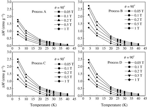
The magnetization hysteresis has been measured as a function of temperature for θ = 0° and 90° and temperatures ranging from 4.2 to 40 K. Figures – show the width of the magnetization hysteresis loops, ΔM, as a function of magnetic field and temperature for all four sample types. Consistently seen in all cases, regardless of temperature, magnetic field or magnetic field angle, is that the samples processed in magnetic field have significantly higher ΔM than the process A samples. Comparing the ΔM data to the transport results shown in figure , it is particularly interesting to note that the transport enhancement from magnetic field processing was only 8.9–9.7%, whereas the enhancement in ΔM, which is proportional to the intragranular critical current density and the size of the current loop, increases by about 80% for process B and about 60% for processes C and D. The differences between processes B, C and D are relatively small, and in particular the differences between C and D, which only vary significantly for θ = 0°.
Figure 7 Width of the magnetization hysteresis loop as a function of magnetic field for all four sample types (a) 4.2 K, θ = 0°; (b) 4.2 K, θ = 90°; (c) 10–40 K, θ = 0°; (d) 10–40 K, θ = 90°.

Figure 8 Width of the magnetization hysteresis loop as a function of temperature for θ = 0°. (a)–(d) Correspond to processes A–D, respectively.
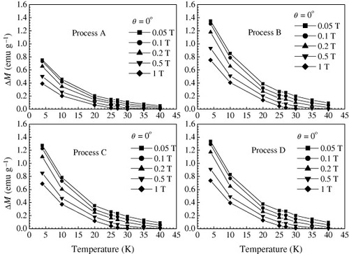
Figure 9 Width of the magnetization hysteresis loop as a function of temperature for θ = 90°. (a)–(d) Correspond to processes A–D, respectively.
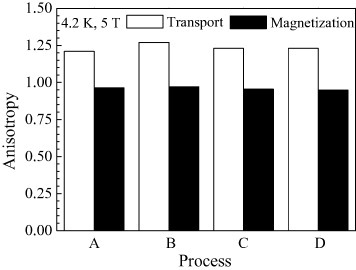
To further understand the results, the electromagnetic anisotropy has been quantified based upon the electrical transport measurements and the magnetization hysteresis measurements. For the former, the anisotropy is defined as the ratio of Ic (θ = 0° )/Ic (θ = 90° ), and for the latter it is the ratio of ΔM(θ = 0° )/ΔM(θ = 90° ). Results for the four sample types are seen in figure . Interestingly, the anisotropy as determined by ΔM is not affected by magnetic field, whereas the electrical transport anisotropy is increased primarily for process B and by a small amount for processes C and D (as could also be seen from figure ).
Figure 10 Electromagnetic anisotropy as determined from electrical transport measurements and magnetization hysteresis measurements.
Microstructure
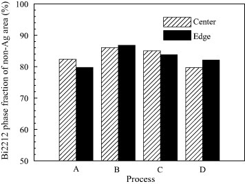
Figures and show backscattered electron (BSE) images of polished cross-sections of samples of all four processing types and from both the edge (initially round filaments, figure ) and the center (initially rectangular filaments, figure ) sections of the wire. In all cases, the microstructure consists of Bi2212, Bi2201 and non-superconducting AEC phases, and significant bridging between filaments which is typical for high performance Bi2212 wires. It appears that the initial filament shape plays a role in how the magnetic field affects Bi2212 growth. In the edge sections of all four sample types (figure ), where the filaments were initially round as found in Bi2212 round wires, the only significant difference between the four sample types is that the samples heat treated in a magnetic field show a reduction in porosity. This is particularly true for the process B and C images. There is no noticeable change in the Bi2212 texture and the growth direction for the Bi2212 bridges that connect the filaments is random. In the center Section (figure ), however, in addition to the reduction in porosity, there is a noticeable change in the Bi2212 interfilamentary bridges. While the bridges in process A remain randomly oriented, those in the process B and C wires have grown predominantly in the direction perpendicular to the applied magnetic field, indicating that the magnetic field affects textured growth primarily during resolidification/nucleation. The eight images in figures and have been analyzed quantitatively with results shown in figure . Plotted is the area percentage of Bi2212 within the non-Ag areas of the wire. These results clearly indicate that the presence of magnetic field during resolidification/Bi2212 nucleation increases the Bi2212 area fraction, whereas magnetic field during solid state growth does not.
Figure 11 Backscattered electron (BSE) images taken within the SEM of filaments in the edge of the wire. (a)–(d) Correspond to processes A–D, respectively.
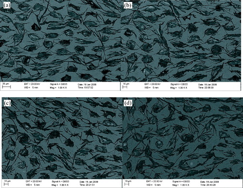
Figure 12 Backscattered electron (BSE) images taken within the SEM of filaments at the center of the wire. (a)–(d) Correspond to processes A–D, respectively.
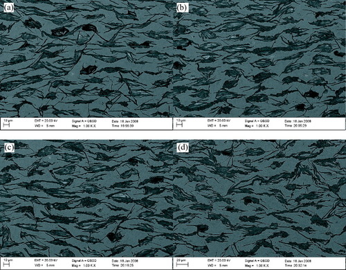
Figure 13 Percentage of Bi2212 in non-Ag areas of processed wires as determined by digital image analysis of the SEM images shown in figures and .
Discussion
The effects of magnetic field on the textured growth of Bi2212 wires have been studied in geometry where, due to the large number of small Bi2212 filaments, the effects of the Bi2212/Ag interface dominate. As a result, the field effects are small relative to past studies on Bi2212 bulk material that lacked Ag altogether, and on monocore tapes, where the Bi2212 volume is large relative to the Bi2212/Ag surface. Nonetheless, some clear and noteworthy effects are observed indicating that magnetic field processing does impact the microstructure and properties of Bi2212 wires. Electrical transport measurements show an improvement in performance when the magnetic field is present during peritectic melting and resolidification. Magnetization hysteresis measurements show an improvement in all samples which experience magnetic field during at least part of the process, with the largest improvement for samples with the magnetic field present throughout the entire process. Changes in the electromagnetic anisotropy, however, are relatively small.
Magnetic field induced texture in Bi2212 superconductors results from the anisotropy in the paramagnetic susceptibility. Therefore, when the oxide is placed in a magnetic field while in the normal state, the magnetic energy is minimized when the axis of maximum susceptibility is parallel to the magnetic field. There are at least four drivers for grain alignment due to magnetic field: (i) rotation of paramagnetic crystals within a liquid phase, (ii) grain nucleation with a preferred orientation, (iii) selective grain growth where grains aligned with their c-axis parallel to the magnetic field preferentially grow at the expense of grains with their c-axis otherwise oriented, (iv) a reduction in quantity of other phases present, resulting in less obstacles to textured growth that is driven by other texturing mechanisms (e.g. the Ag interface). It remains difficult to fully assess which of these mechanisms dominate.
Ferreira et al [Citation47, Citation48] proposed a model to explain magnetic field induced texture, which suggests that the enhancement in texture is primarily due to grain rotation during the early stages of crystal growth from the liquid. During the nucleation of crystals from the melt, when the crystals achieve a critical volume and are still surrounded by a large liquid volume fraction, the magnetic driving force is capable of introducing grain rotation. At the later stages of growth, however, the presence of nearby grains introduces grain-to-grain interactions that hinder magnetic field induced alignment. If this is correct, then in this investigation, due to the relatively small Bi2212 filaments (∼ 25 μ m), the effect of magnetic field on the Bi2212 may be limited to the nucleation and growth processes, leading to the effect of the magnetic field during processes B and C to be dominant. This is consistent with the transport results and with the enhanced orientation of the Bi2212 bridges seen in the SEM images. Rotation of superconductor grains requires both the anisotropy of magnetic susceptibility and the coexistence of liquid which can be a lubricant for grain rotation, or at least be of low enough viscosity not to prevent rotation. While it is likely that some liquid phase is formed at the beginning of the second heat treatment during split melt processing, it is also known that multiple phases other than Bi2212 exist after the first heat treatment, including AECs, Cu-free phases and Bi2201. Thus, the mechanical interaction between superconductor grains and these second phases may obstruct Bi2212 grain rotation despite the presence of some liquid, inhibiting texturing.
The improvement in magnetization hysteresis, without any change in magnetically measured anisotropy, implies that the magnetic field during processing impacts more than just textured grain growth. Magnetic hysteresis is caused by intragranular shielding currents flowing in individual superconducting grains as well as by intergranular currents flowing across grain boundaries. In the case of textured materials, the anisotropy of the properties represents an additional parameter to be considered for understanding the magnetization results. The absence of significant change in the magnetization anisotropy, with a clear increase in the bulk magnetization and an increased sharpness of the magnetic transition, is consistent with the hypothesis that the presence of magnetic field affects the phase assemblage such that a larger volume fraction of higher density Bi2212 results. This does not explain the improved texturing of the interfilamentary bridges, but the bridges represent a small fraction of the total amount of Bi2212 present and thus play a relatively small role in the magnetization behavior, even if they play a significant role in the transport behavior by interconnecting filaments. Thus, it appears that at least two mechanisms exist, one which increases texturing within filaments and of interfilamentary bridges, and another which improves the Bi2212 volume fraction and density.
It is important to recognize that the effects of magnetic field processing depend on the initial filament shape, with significant impact on the rectangular filaments and less impact on round filaments. This is understood in the context of the important role of the Ag/Bi2212 interface in Bi2212 nucleation and microstructural development. It is possible that bridges grow along certain crystallographic Ag planes which are energetically favorable and that the Ag texture may affect Bi2212 grain alignment [Citation49]. Thus, the effect of the magnetic field on filament bridging may be a combined effect of the magnetic field on Ag, Bi2212 and the Ag/Bi2212 interface. This supports the hypothesis that the magnetic field affects the phase assemblage (supported by the image analysis) and that the modified phase assemblage (reduced non-superconducting phases) improves the oriented growth by not blocking grain growth. In this case the dominant texturing mechanism may be the Ag interface rather than the magnetic field itself. This requires further investigation. Although Liu et al have shown that the c-axis of Bi2212 grains grow parallel to the magnetic field regardless of the Bi2212/Ag interface orientation [Citation50], this study was not performed on multifilamentary wires with small filaments, where the ratio of the interfacial area to the Bi2212 volume is large.
Summary and conclusions
The application of magnetic field during varying segments of split melt-processing in low aspect ratio Bi2212/AgMg multifilamentary rectangular wire resulted in enhanced electrical and magnetic behavior, small changes in the electrical anisotropy, no change in the magnetic anisotropy, and an altered microstructure, particularly in the regions of the wire with rectangular filaments. These results indicate that at least two mechanisms are at work. One mechanism is an altered phase assemblage that leads to higher volume fraction and higher density Bi2212 grains and is responsible in part for the improved magnetization hysteresis behavior. The second mechanism improves textured grain growth, particularly in the interfilamentary bridges that, despite being a relatively small fraction of the Bi2212 present, play an important role in electrical transport.
Acknowledgments
The authors thank Bill Nachtrab and Terry Wong from Supercon, Inc., for Bi2212 wires, Ulf Trociewitz for many useful discussions, and Quang V. Le for image analysis.
References
- ChoiE SBrooksJ SEatonD LAlPHaikM SHussainiM YGarmestaniHLiDDahmenK J. Appl. Phys. 94 6034 http://dx.doi.org/10.1063/1.1616638
- LudtkaG MJaramilloR AKisnerR ANicholsonD NWilgenJ BLudtkaGKaluP N 2004 Scr. Mater. 51 171 http://dx.doi.org/10.1016/j.scriptamat.2004.03.029
- NoudemJ G 1996 Physica C 264 325 http://dx.doi.org/10.1016/0921-4534(96)00273-0
- YasudaHTokiedaKOhnakaI 2000 Mater. Trans. JIM 41 1005
- LegrandB AChateignerDPerrier de laBathieRTournierR 1997 J. Magn. Magn. Mater. 73 20 http://dx.doi.org/10.1016/S0304-8853(97)00149-2
- EnomotoMTazukeY 2001 Metall. Mater. Trans. A 32 445 http://dx.doi.org/10.1007/s11661-001-0061-6
- ShimotomaiMMineK 2003 Acta Mater. 51 2921
- HaradaKTsurekawaSWatanabeTPalumboG 2003 Scr. Mater. 49 367 http://dx.doi.org/10.1016/S1359-6462(03)00329-4
- TaniguchiTSassaKYamadaTAsaiS 2000 Mater. Trans. JIM 41 981
- AwajiSWatanabeKMaYMotokawaM 2001 Physica B 294–295 482 http://dx.doi.org/10.1016/S0921-4526(00)00705-5
- CasavamtM JWaltersD ASchmidtJ JSmalleyR E 2003 J. Appl. Phys. 93 2153 http://dx.doi.org/10.1063/1.1536732
- Committee on Opportunities in High Magnetic Field Science 2005 Opportunities in High Magnetic Field Science Washington, DC National Research Council
- KumakuraHToganoKDietderichD RMaedaHKaseJMorimotoT 1991 IEEE Trans. Magn. 27 1250 http://dx.doi.org/10.1109/20.133411
- WeijersH WHuQ YHascicekY SGodekeAVouchkovYCelikESchwartzJMarkenKDaiWParrellJ 1999 IEEE Trans. Appl. Supercond. 9 563 http://dx.doi.org/10.1109/77.783358
- WeijersH WSchwartzJten HakenBDhalleMten KateH H J 2003 Supercond. Sci. Technol. 16 672 http://dx.doi.org/10.1088/0953-2048/16/6/303
- WeijersH WTrociewitzU PMarkenKMeineszMMiaoHSchwartzJ 2004 Supercond. Sci. Technol. 17 636 http://dx.doi.org/10.1088/0953-2048/17/4/012
- KesslerJBoutemySChenSDimapilisDMillerVWeiWSchwartzJ 1997 IEEE Trans. Appl. Supercond. 7 1560 http://dx.doi.org/10.1109/77.620872
- MaedaHOhyaKSatoMChenW PWatanabeKMotokawaMMatsumotoAKumakuraHSchwartzJ 2002 Physica C 382 33 http://dx.doi.org/10.1016/S0921-4534(02)01192-9
- HellstromE ERayR D 1995 Physica C 251 27 http://dx.doi.org/10.1016/0921-4534(95)00368-1
- MiaoHMarkenK RMeineszMCzabajBHongSTwinANoonanPTrociewitzU PSchwartzJ 2007 IEEE Trans. Appl. Supercond. 17 2262 http://dx.doi.org/10.1109/TASC.2007.898999
- MarkenK R JrMiaoH PMeineszMCzabajBHongS 2006 IEEE Trans. Appl. Supercond. 16 992 http://dx.doi.org/10.1109/TASC.2006.873262
- SchwartzJ et al 2008 IEEE Trans. Appl. Supercond. 18 70 http://dx.doi.org/10.1109/TASC.2008.921363
- KaseJMorimotoTToganoKKumakuraHDietderichD RMaedaH 1991 IEEE Trans. Magn. 27 1254 http://dx.doi.org/10.1109/20.133412
- JinSTiefelT MScherwoodR CDeverR BDavisM EKammolttG WFastnachtR A 1987 Phys. Rev. B 37 7850 http://dx.doi.org/10.1103/PhysRevB.37.7850
- LabordeOTholenceJ LLejayPSulpiceATournierRCapponiJ JMichelCProvostJ 1987 Solid State Commun. 63 887 http://dx.doi.org/10.1016/0038-1098(87)90330-9
- HagbergJLeppavuoriSUusimakiA 1993 Physica C 216 325 http://dx.doi.org/10.1016/0921-4534(93)90076-3
- MaedaHSastryPTrociewitzU PSchwartzJOhyaKSatoM 2003 IEEE Trans. Appl. Supercond. 13 3339 http://dx.doi.org/10.1109/TASC.2003.812309
- MaedaHSastryP P S STrociewitzU PSchwartzJOhyaKSatoMChenW PWatanabeKMotokawaM 2003 Physica C 386 115 http://dx.doi.org/10.1016/S0921-4534(02)02237-2
- RamosM ALiuX TShenT MTrociewitzU PSchwartzJ 2007 IEEE Trans. Appl. Supercond. 17 3103 http://dx.doi.org/10.1109/TASC.2007.898876
- XuBSuJ HSchwartzJ 2005 Supercond. Sci. Technol. 18 503 http://dx.doi.org/10.1088/0953-2048/18/4/020
- DiezJ CAngurelL AMiaoHFernadezJ Mde la FuenteG F 1998 Supercond. Sci. Technol. 11 101 http://dx.doi.org/10.1088/0953-2048/11/1/020
- HayashiKNonoyamaHNagataMHitotsuyanagiH 1990 Supercond. Sci. Technol. 3 81 http://dx.doi.org/10.1088/0953-2048/3/2/006
- SoyluBAdamopoulosNGlowackiD MEvettsJ E 1992 Appl. Phys. Lett. 60 3183 http://dx.doi.org/10.1063/1.106736
- EickemeyerJSelbmannDOpitzRMaherEPrusseitW 2000 Physica C 341–348 2425 http://dx.doi.org/10.1016/S0921-4534(00)01145-X
- EmV 2003 Supercond. Sci. Technol. 16 498 http://dx.doi.org/10.1088/0953-2048/16/4/313
- Nekkanti et al 2001 IEEE Trans. Appl. Supercond. 11 3321 http://dx.doi.org/10.1109/77.919773
- GoyalA et al 1996 Appl. Phys. Lett. 69 1795 http://dx.doi.org/10.1063/1.117489
- PavardSBourgaultDVillardCTournierR 1999 Physica C 316 198 http://dx.doi.org/10.1016/S0921-4534(99)00259-2
- ShenT MLiuX TTrociewitzU PNachtrabW TWongTSchwartzJ 2008 IEEE Trans. Appl. Supercond. 18 520 http://dx.doi.org/10.1109/TASC.2008.921360
- SchwartzJMerrittG A 2007 Supercond. Sci. Technol. 20 L59 http://dx.doi.org/10.1088/0953-2048/20/10/L02
- LiuX TShenT MTrociewitzU PSchwartzJ 2008 IEEE Trans. Appl. Supercond. 18 1179 http://dx.doi.org/10.1109/TASC.2008.922258
- NachtrabW TRenaudC VWongTLiuX TShenT MTrociewitzU PSchwartzJ 2008 IEEE Trans. Appl. Supercond. 18 1184 http://dx.doi.org/10.1109/TASC.2008.920630
- BourgaultBFlahautEAntoneviciABruzekC ELallouetNSoubeyrouxJ LTournierR 2004 Supercond. Sci. Technol. 17 463 http://dx.doi.org/10.1088/0953-2048/17/3/027
- van der LaanD Cvan EckH J Nten HakenBSchwartzJten KateH H J 2002 Physica C 372–376 1024 http://dx.doi.org/10.1016/S0921-4534(02)00962-0
- van der LaanD CSchwartzJten HakenBDhalleMvan EckH J N 2008 Phys. Rev. B 77 104514 http://dx.doi.org/10.1103/PhysRevB.77.104514
- KumakuraHToganoKMaedaHYanagisawaEMorimotoT 1989 Japan. J. Appl. Phys. 28 L176 http://dx.doi.org/10.1143/JJAP.28.L176
- FerreiraP JLiuH BSandeJ B V 1999 IEEE Trans. Appl. Supercond. 9 2231 http://dx.doi.org/10.1109/77.784913
- FerreiraP JLiuH BSandeJ B V 1999 J. Mater. Res. 14 2751 http://dx.doi.org/10.1557/JMR.1999.0368
- MatsumotoAKitaguchiHKumakuraHToganoK 2000 Physica C 341–348 2435 http://dx.doi.org/10.1016/S0921-4534(00)01157-6
- LiuH BFerreiraP JSandeJ B V 1998 Physica C 303 161 http://dx.doi.org/10.1016/S0921-4534(98)00250-0