Abstract
A zero-gap state with a Dirac cone type energy dispersion was discovered in the organic conductor α-(BEDT-TTF)2I3 under high hydrostatic pressures. This is the first two-dimensional (2D) zero-gap state discovered in bulk crystals with a layered structure. In contrast to the case of graphene, the Dirac cone in this system is highly anisotropic. The present system, therefore, provides a new type of massless Dirac fermion system with anisotropic Fermi velocity. This system exhibits remarkable transport phenomena characteristic to electrons on the Dirac cone type energy structure. The carrier density, written as n∝T2, is a characteristic feature of the 2D zero-gap structure. On the other hand, the resistivity per layer (sheet resistance RS) is given as RS=h/e2 and is independent of temperature. The effect of a magnetic field on samples in the zero-gap system was examined. The difference between zero-gap conductors and conventional conductors is the appearance of a Landau level called the zero mode at the contact points when a magnetic field is applied normal to the conductive layer. Zero-mode Landau carriers give rise to strong negative out-of-plane magnetoresistance.
Introduction
Since Novoselov et al [Citation1] and Zhang et al [Citation2] experimentally demonstrated that graphene is a zero-gap system with massless Dirac particles, such systems have fascinated physicists as a source of exotic systems and new physics. At the same time, the quasi-two-dimensional (2D) organic conductor α-(BEDT-TTF)2I3 (BEDT-TTF=bis(ethylenedithio) tetrathiafulvalene) was found to be a new type of massless Dirac fermion state under high pressures [Citation3–6]. Originally, this material had been considered as a narrow-gap semiconductor [Citation7–9]. In contrast to graphene, this is the first bulk (multilayer) zero-gap material with a Dirac cone type energy dispersion. In this review, we describe the remarkable transport phenomena characteristic to electrons on the Dirac cone type energy structure in α-(BEDT-TTF)2I3 under high pressure [Citation5–8].
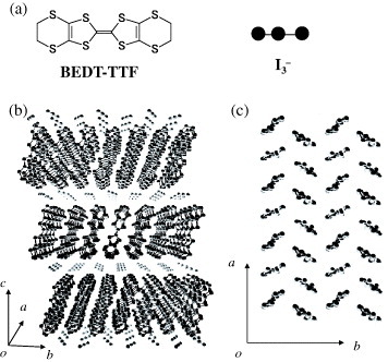
The organic conductor α-(BEDT-TTF)2I3 is a member of the ((BEDT-TTF)2I3 family [Citation10]. All the crystals in this family consist of conductive layers of BEDT-TTF molecules and insulating layers of I3− anions as shown in figure [Citation10–13]. The difference among them lies in the arrangement and orientation of BEDT-TTF molecules within the conducting plane, and this difference gives rise to variations in the transport phenomena. Most of the members of this family are 2D metals with large Fermi surfaces, and some of them are superconducting with Tc values of several Kelvin [Citation11–13]. On the other hand, α-(BEDT-TTF)2I3 differs from the other crystals. According to the band calculation, this system is a semimetal with two small Fermi surfaces; one with electron character and the other with hole character [Citation8].
Figure 1 (a) BEDT-TTF molecule and I3- molecule. (b) Crystal structure of α-(BEDT-TTF)2I3 viewed along the a-axis. (c) Crystal structure viewed along the c-axis. (From [Citation5].)
When cooled, it behaves as a metal above 135 K, where it undergoes a phase transition to an insulator as shown in figure [Citation10]. In the insulator phase below 135 K, the rapid decrease in the magnetic susceptibility indicates that the system is in a nonmagnetic state with a spin gap [Citation14]. According to the theoretical work by Kino and Fukuyama [Citation15] and Seo [Citation16] and the experimental investigation by Takano et al (nuclear magnetic resonance) [Citation17] and Wojciechowski et al (Raman) [Citation18], this transition is due to the charge disproportionation. At temperatures below 135 K, horizontal charge stripe patterns for +1e and 0 have been formed as shown in the inset of figure .
Figure 2 Temperature dependence of the resistance under several hydrostatic pressures [Citation5, Citation8]. The inset shows a schematic picture of the arrangement of BEDT-TTF molecules in a conducting layer viewed from the c-crystal axis and the charge pattern under ambient pressure. At temperatures below 135 K, the BEDT-TTF molecule layer forms horizontal charge stripe patterns for +1e and 0 [Citation15–18]. (From [Citation5].)
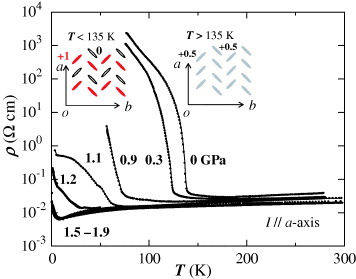
When the crystal is placed under a high hydrostatic pressure of above 1.5 GPa, the metal–insulator transition is suppressed and the metallic region expands to low temperatures as shown in figure [Citation7, Citation19, Citation20]. This change in the electronic state is accompanied by the disappearance of the charge-ordering state as shown by the Raman experiment [Citation18]. Note that in the high-pressure phase, the resistance is almost constant between 300 and 2 K. It looks like a dirty metal with a high density of impurities or lattice defects. In dirty metals, the mobilities of carriers are low and depend on temperature only weakly, and therefore, resistance is also independent of temperature. In the present case, however, the situation is different. Carriers with a very high mobility ∼105 cm Vs−1 exhibit extremely large magnetoresistance at low temperatures [Citation5, Citation7, Citation8, Citation19], indicating that the crystal is clean.
To clarify the mechanism of these apparently contradictory phenomena, the Hall effect was first examined by Mishima et al [Citation20]. However, the magnetic field of 5 T they used was too high to investigate the property of carriers in the zero-field limit. This is because the carrier system at low temperatures is sensitive to the magnetic field and its character is varied even in weak magnetic fields below 1 T. Thus, Tajima et al [Citation8] reexamined the Hall effect using a much lower magnetic field of 0.01 T. They also investigated the magnetoresistance and Hall resistance as a function of the magnetic field up to 15 T and the temperature between 0.5 and 300 K. The experimental results they obtained are summarized as follows:
Under a pressure of above 1.5 GPa, the resistivity is nearly constant between 300 and 2 K [Citation5, Citation8, Citation20].
In the same temperature range, both the carrier (hole) density and the mobility change by about six orders of magnitude. At low temperatures below 4 K, the carrier system is in a state with a low density of about 8×1014 cm−3 and a high mobility of about 3×105 cm2 Vs−1 [Citation5, Citation8].
The changes in the density and mobility cancel each other to give a constant resistance [Citation5, Citation8, Citation20].
At low temperatures, the resistance and Hall resistance are very sensitive to the magnetic field [Citation5, Citation7, Citation8, Citation19]. However, neither quantum oscillations nor the quantum Hall effect were observed in magnetic fields up to 15 T [Citation5].
The system is not a metal but a semiconductor with an extremely narrow energy gap of less than 1 meV [Citation5, Citation7].
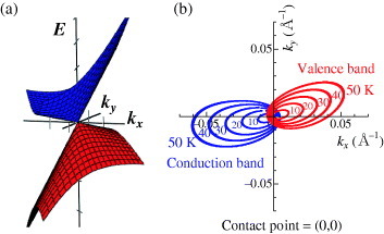
Figure 3 (a) Band structure and (b) energy contours near a contact point. They are calculated using the parameters for p=0.6 GPa in [Citation4]. Note that the origin of the axes is taken at the contact point. (From [Citation6].)
The picture of the zero-gap system improve understanding of the remarkable transport phenomena of α-(BEDT-TTF)2I3, which are described and interpreted in this paper.
Temperature dependence of the carrier density and mobility
First, let us discuss the temperature dependence of the carrier density and mobility in this material under high pressures.
For a detailed quantitative analysis, we refer to figure where the mobilities of electrons and holes, μe and μh, respectively, are plotted against the temperature together with the carrier density. These quantities were deduced from the experimental data based on five assumptions:
The system is strictly 2D.
There is no interaction between conductive layers.
The densities of electrons and holes are equal (intrinsic semiconductor).
The Fermi energy does not change with temperature.
The mobilities of electrons and holes are isotropic relatively to the current direction in the conductive layer.
Figure 4 Temperature dependence of the carrier density and mobility. The data plotted by black dots are the effective carrier density (neff) and mobility (μeff) estimated from the Hall coefficient and conductivity. The magnetoresistance mobility (μM) from 77 to 2 K is shown by squares □. Assuming this is the simplest 2D system, we can separate the mobility of electrons (μe) and holes (μh) from the equations μeff=μh−μe and μM2=μe·μh. The real density (n: blue triangles) of electrons and holes, on the other hand, is calculated as . (From [Citation6].)
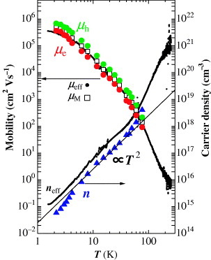
In the simplest two-carrier picture, the effective mobility μeff and magnetoresistance mobility μM are expressed in terms of the electron mobility μe and hole mobility μh as μeff=μh−μe and μM2=μh·μe. The μeff is calculated by combining the Hall coefficient RH with the conductivity σ (μeff=σRH). The μM, on the other hand, is defined as M=(μMB)2 in a low magnetic field, where M=Δρ0/ρ0=(ρ(B)−ρ0)/ρ0 is the magnetoresistance. Thus, using the experimental values of μeff and μM, one can determine μh and μe. On the other hand, the density of electrons and holes (n=ne=nh) is calculated as , where neff is the effective carrier density determined from the Hall coefficient RH as neff=1/RHe.
This analysis was performed at temperatures below 77 K. Above this temperature, the magnetoresistance could not be detected with sufficient accuracy.
Let us examine the temperature dependence of the carrier density. Between 77 and 2 K, it decreases by about four orders of magnitude as shown in figure . This large reduction of the carrier density is characteristic of semiconductors. However, the temperature dependence differs from those of the ordinary semiconductors. In ordinary semiconductors with finite energy gaps, the carrier density depends exponentially on the inverse temperature. On the other hand, the data in figure show a power-law temperature dependence n∝Tα, with α≃2. This temperature dependence of carrier density is explained considering a 2D zero-gap system with a linear energy dispersion as follows.
The carrier density is given by
where D(E) is the density of states and f0(E) is the Fermi distribution function. For electrons on the anisotropic cone with the energy dispersion given by equation (Equation1
),
, the density of states is expressed as
Here the energy E is measured from the contact point and
is an average of vF(φ) defined by
It is important to note that in this system, the Fermi energy EF is located at the contact point and does not move with temperature. Therefore, EF=0. This is because the system is an intrinsic semiconductor with no intentional carrier doping. The symmetry of the energy structure with respect to the contact point also plays an important role in fixing the Fermi energy. Thus, the carrier density is given as
where c=1.75 nm is the lattice constant along the direction normal to the 2D plane. This relation n∝T2 fits the temperature dependence of carriers from 77 to 2 K. The averaged value of the Fermi velocity,
is estimated as
. This value corresponds well to the result obtained from realistic theories [Citation4, Citation23]. Thus, we can show that the carrier density of this system obeys n(T)∝T2, which expresses the carrier density of 2D zero-gap conductors.
Another characteristic feature of the zero-gap system is the electron–hole symmetry. This is due to the energy structure of the Dirac cone, which is symmetrical around the contact point. We can see this effect in the temperature dependences of μe, μh in figure . In the wide temperature range between 77 and 2 K, where both μe and μh change by about four orders of magnitude, the difference between μh and μe at each temperature is within a factor of 2. This effect, ascribable to the electron–hole symmetry, is a further evidence of the system being a zero-gap conductor. The small but finite discrepancy, however, indicates that the symmetry is not perfect.
Temperature-independent resistivity
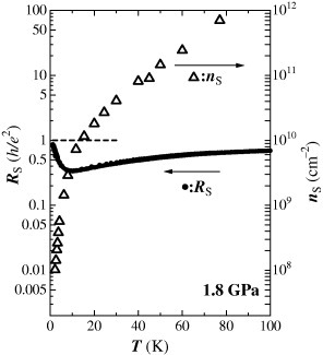
The most interesting phenomenon observed in this material is the temperature independence of electrical resistance. This is astonishing because the carrier density varies by four orders of magnitude between 77 and 2 K. To address the mechanism of this anomalous phenomenon, we refer to figure which shows the resistivity per layer (sheet resistance RS). Note that a conductive layer of this material is sandwiched by insulating layers as shown in figure , and therefore, each conductive layer is almost independent. Thus, the concept ‘resistivity per layer’ is valid for this system. In this figure, it is shown that the sheet resistance depends on the temperature very weakly except for below 7 K. Note that the sheet resistance is close to the quantum resistance, h/e2=25.8 kΩ. It varies from a value approximately equal to the quantum resistance at 100 K to about 1/5 of it at 7 K. The reproducibility of data was checked using six samples. Such behavior of the resistance is one of the characteristics of zero-gap semiconductors. This phenomenon is understood qualitatively as follows.
Figure 5 Temperature dependence of the sheet resistance (RS). Note that the data include a systematic error within a factor of 2, which mainly arises from the difficulty of accurate measurement of the sample dimensions. In the figure, we also plotted the temperature dependence of carrier density per layer (nS). (From [Citation6].)
When an electric field is applied to carriers on a Dirac cone along the x-axis, the Boltzmann transport equation gives the conductivity as
where f0(k) is the Fermi function in the thermal equilibrium and τ(E) is the scattering lifetime, which is assumed to depend on the energy of the carriers. Substituting vx=vF cos(φ) and integrating over φ, we obtain
Then, we replace vFτ(E) with the mean free path l(E) and adopt Mott's argument [Citation24]. It states that the mean free path of a carrier subjected to elastic scattering can never be shorter than the carrier wavelength; thus l(E)k1. In this case, the density of scattering centers is high, l(E)k∼1. Substituting these relations into the above expression for σxx and changing the variable from k to E, the integration is performed. The result is
Many realistic theories predict that the sheet resistance of intrinsic zero-gap systems is given as RS=gh/e2, where the parameter g∼1 [Citation25–27]. Thus, the constant resistance observed in this material is ascribed to a zero-gap energy structure.
Here, we mention the localization of carriers in this system. As shown in figures and , the carrier density at 2 K is only 108 cm−2/sheet (figure ). However, the carriers are not localized but mobile with a mobility as high as 105 cm2 Vs−1 (figure ). This is one of the characteristic features of carriers on a Dirac cone.
Electron system in the magnetic field
One of the characteristic properties of this material is that the carrier system has extremely low density and high mobility in the lowest-temperature region (figure ). Such a highly mobile carrier system should be sensitive to the magnetic field.
The magnetotransport phenomena of α-(BEDT-TTF)2I3 were first investigated by Ojiro et al. They discovered an anomalously large magnetoresistance and the buildup of a large Hall voltage at low temperatures when a magnetic field is applied normal to the 2D plane [Citation7, Citation19]. In this section, we discuss the carrier states of α-(BEDT-TTF)2I3 in a magnetic field.
Figure (a) shows the temperature dependence of the resistance in magnetic fields up to 15 T at a pressure of 1.8 GPa [Citation5]. In the absence of the magnetic field, the resistance decreases with decreasing temperature down to 10 K, where it starts to increase. In a magnetic field, the resistance begins to increase at a higher temperature. Following this rise, a shoulder appears and then a step-like flat region. At 1 T, for example, the shoulder is located at about 6 K. When the magnetic field is high, another shoulder appears at lower temperatures. In the curve for 10 T, the first shoulder is at 15 K and the second shoulder is around 2 K. In figure (b), the resistance is plotted as a function of magnetic field with the temperature fixed [Citation5]. Two step structures can be clearly recognized. At 2 K, the resistance rises with magnetic fields below 0.1 T and the subsequent saturation is observed (upper panel of the figure). The flattening of the curve for 0.2 T forms the first shoulder. The curve starts to increase again at a field of 3 to 4 T and then a second shoulder appears at a field of 8 to 10 T (main panel).
Figure 6 (a) Temperature dependence of the resistance under a magnetic field up to 15 T. (b) Magnetic field dependence of the resistance down to 0.5 K. The low-field region below 1 T is shown in the inset. (From [Citation5].)
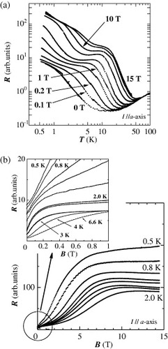
These experimental data suggest that with increasing magnetic field or decreasing temperature, the system changes from a ‘low-resistance’ state to a ‘intermediate-resistance’ state and then to a ‘high-resistance’ state as shown in figure , where the boundaries between the states in the B-T plane are depicted using the data in figure .
Figure 7 Schematic diagram of boundaries between ‘low-resistance’, ‘intermediate-resistance’ and ‘high-resistance’ states in the B-T plane.
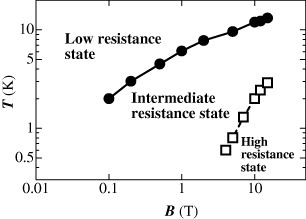
A naive interpretation of the phenomena described above is to assume that near the Fermi energy, different types of carriers exist and that the transport phenomena reflect the character of carriers giving the dominant contribution to the transport. The transport phenomena in the low-resistance state can be ascribed to the carrier system related to the Dirac cone as mentioned above. On the other hand, what is the origin of the other two electron systems? Judging from the experimental results, which indicate that the mobility is low, they will have much heavier mass than that of carriers on the Dirac cone.
Remarkable is the appearance of a Landau level in such a zero-gap state at the contact points when a magnetic field is applied normal to the conductive layer [Citation28]. Since the energy of this level is EF irrespective of the field strength, the Fermi distribution function is always 1/2. This means that half the Landau states, which are degenerate in the zero mode, are occupied. Landau degeneracy is proportional to the strength of the magnetic field B, and therefore it can large in high magnetic fields. Recently, Osada pointed out that this effect should be detected in the out-of-plane resistance in a transverse magnetic field [Citation29]. The field parallel to the current does not exert the Lorentz force on carriers; thus, the motion of carriers in the current direction is not affected by the magnetic field. Hence, the conductivity in this direction is proportional to the carrier density. The effect of a magnetic field only appears if the carrier density changes.
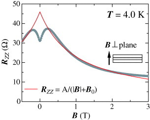
To demonstrate the appearance of zero-mode Landau carriers, the out-of-plane resistivity of this zero-gap conductor was examined in the magnetic field. Figure shows the magnetic field dependence of out-of-plane magnetoresistance in a magnetic field normal to the 2D plane at 4 K [Citation30]. The resistivity increases with the magnetic fields below 0.2 T and then starts to decrease. The drop of the resistivity is large. In the field of 3 T, the resistivity is about 1/3 of that at 0.2 T.
Figure 8 Magnetic field dependence of the interlayer resistance under a pressure of about 1.7 GPa at 4 K. As for negative magnetoresistance in fields above 0.5 T, the data were fitted with a formula Rzz∝1/(|B|+B0) (red solid line), where B0=0.7 T.
We consider that this large negative magnetoresistance can be ascribed to zero-mode Landau carriers. The existence of the zero-mode Landau level is one of the characteristic properties in zero-gap conductors with Dirac cones. To understand the effect of zero-mode Landau carriers, we should examine them quantitatively. First, we look at the energy of Landau levels in zero-gap systems expressed as , where vF is the Fermi velocity and n is the Landau index [Citation28]. Among the Landau levels, the one with n=0 (zero mode) gives the dominant contribution to the low-temperature transport phenomena because other Landau levels are far from the Fermi energy. At 1 T, for example, the Landau level with n=1 is about 30 K when vF=107 cm s−1, estimated from the temperature dependence of carrier density. In this case, at temperatures below 30 K, most of the mobile carriers are in the zero-mode Landau level. Such a situation is known as a quantum limit. Note that these Landau levels agree with the realistic theory by Goerbig et al [Citation23].
The out-of-plane resistivity is proportional to the carrier density, which in the quantum limit is given as D(B)=1/2·B/φ0, where φ0=h/e is the quantum flux. The factor 1/2 is the Fermi distribution function at EF. In moderately strong magnetic fields, the density of magnetic-field-induced carriers can be very high. By examining the Hall effect, the density of zero-mode carriers was estimated as ∼1012 cm−2 in a field of 3 T at 4 K [Citation5]. This value is about 2 orders of magnitude higher than the density of thermally excited carriers at 4 K, and in the absence of a magnetic field, it is 108 cm−2. The carrier density in a magnetic field is proportional to the magnetic field. Thus, this large change in the carrier density will be detectable as a change in the resistance.
Recently, Osada gave an analytical formula for the out-of-plane magnetoresistance in a multilayer Dirac fermions system [Citation29]. For a magnetic field normal to the 2D plane, the formula can be simplified to ρzz=A/(|Bz|+B0), where is a field-independent constant in the case of a pure system, tc is the inter-layer transfer energy, B0 is a fitting parameter that depends on the quality of the crystal and C is defined by C=∫ρ0(E)(−df/dE)dE, using the spectral density of the zero-mode Landau level ρ0(E), which satisfies ∫ρ0(E)dE=1 [Citation29]. Note that only the lattice constant c is a material parameter. This simple formula closely reproduces the magnetic field dependence of the magnetoresistance in a magnetic field of above 0.5 T as shown in figure . Here, B0 was taken as 0.7 T [Citation30].
Below 0.2 T, on the other hand, the formula disagrees with the data. This is because the model is oversimplified. The formula is based on the quantum-limit picture, in which only the zero-mode Landau level at the Fermi level is considered. In fact, each Landau level is broadened by scattering, zero-mode Landau level is certain to overlap with other Landau levels at low magnetic fields. In the present system, the overlap between the zero mode and other Landau levels should be sufficiently small in magnetic fields of above 0.2 T and, as a result, negative magnetoresistance is observed at 4 K. In fact, at 0.2 T, the energy of the n=1 Landau level of about 12 K is sufficiently large compared with the thermal energy 2kBT=8 K.
Concluding, zero-mode Landau carriers exist in α-(BEDT-TTF)2I3 at low temperatures, under high pressures, in a magnetic field. This material shows strong negative out-of-plane magnetoresistance. Figures and suggest that this region corresponds to the intermediate-resistance state, where the first shoulder was observed in the in-plane magnetoresistance. A quantitative explanation of the in-plane magnetotransport phenomena (ρxx and ρxy) of this system will be published elsewhere.
Finally, we mention the Zeeman effect in this system, which was not considered in the above discussion. Zeeman effect splits the energy of Landau energies EnLL into ±ΔE. At low temperatures, where kBT<ΔE, this effect reduces the density of zero-mode carriers. Recently, Tajima et al [Citation30] demonstrated that the out-of-plane resistivity obeys the exponential law Rzz∝exp(μBB/kBT) at temperatures down to 60 mK. This region is the high-resistance state in figure .
Conclusions
Under high hydrostatic pressure, α-(BEDT-TTF)2I3 is an intrinsic zero-gap semiconductor with a Dirac type energy band. The carrier density, expressed as n∝T2, is a characteristic feature of the zero-gap system. On the other hand, the resistance remains constant from 2 to 300 K. The sheet resistance can be written in terms of the quantum resistance h/e2 as RS=gh/e2, where the parameter g weakly depends on temperature. In graphite systems, a monolayer sample (graphene) is necessary to realize a zero-gap state. On the other hand, it was demonstrated on example of the present system that bulk crystals can show 2D zero-gap behavior. This effect can be observed in the out-of-plane magnetoresistance. The existence of the zero-mode Landau level is a characteristic feature of the zero-gap system. The effect of Landau degeneracy, which is proportional to the strength of the magnetic field, gives rise to the large negative magnetoresistance.
α-(BEDT-TTF)2I3 provides us with a testing ground for a new type of quasi-particles, that is massless Dirac fermions with anisotropic Fermi velocity. The parameter of the anisotropic Dirac cone can be examined using the analytical formula for negative out-of-plane magnetoresistance (figure ) by Morinari et al [Citation31] and/or that for in-plane magnetoresistance (figure ) by Goerbig et al [Citation32].
Acknowledgments
We are grateful to Dr S Sugawara, Professor M Tamura, Dr R Kato, Professor Y Nishio and Professor Y Iye for fruitful collaborations which helped us understand the subjects discussed in this paper. We thank Professor T Osada, Dr A Kobayashi, Dr S Katayama, Professor Y Suzumura, Dr R Kondo, Dr T Morinari, Professor T Tohyama and Professor H Fukuyama for valuable discussions. This work was supported by Grant-in-aid for Scientific Research (No. 19540387) from the Ministry of Education, Culture, Sports, Science and Technology, Japan.
References
- NovoselovK SGeimA KMorozovS VJiangDKatsnelsonM IGrigorievaI VDubonosS VFirsovA A 2005 Nature 438 197 http://dx.doi.org/10.1038/nature04233
- ZhangYTanY WStormerHKimP 2005 Nature 438 201 http://dx.doi.org/10.1038/nature04235
- KobayashiAKatayamaSNoguchiKSuzumuraY 2004 J. Phys. Soc. Japan 73 3135 http://dx.doi.org/10.1143/JPSJ.73.3135
- KatayamaSKobayashiASuzumuraY 2006 J. Phys. Soc. Japan 75 054705 http://dx.doi.org/10.1143/JPSJ.75.054705
- TajimaNSugawaraSTamuraMNishioYKajitaK 2006 J. Phys. Soc. Japan 75 051010 http://dx.doi.org/10.1143/JPSJ.75.051010
- TajimaNSugawaraSTamuraMKatoRNishioYKajitaK 2007 Europhys. Lett. 80 47002 http://dx.doi.org/10.1209/0295-5075/80/47002
- KajitaKOjiroTFujiiHNishioYKobayashiHKobayashiAKatoR 1993 J. Phys. Soc. Japan 61 23
- TajimaNTamuraMNishioYKajitaKIyeY 2000 J. Phys. Soc. Japan 69 543 http://dx.doi.org/10.1143/JPSJ.69.543
- TajimaNEbina-TajimaATamuraMNishioYKajitaK 2002 J. Phys. Soc. Japan 71 1832 http://dx.doi.org/10.1143/JPSJ.71.1832
- BenderKHennigISchweitzerDDietzKEndresHKellerH J 1984 Mol. Cryst. Liq. Cryst. 108 359 http://dx.doi.org/10.1080/00268948408078687
- ShibaevaR PKaminskiiV FYagubskiiE B 1985 Mol. Cryst. Liq. Cryst. 119 361 http://dx.doi.org/10.1080/00268948508075186
- KobayashiHKatoRKobayashiANishioYKajitaKSasakiW 1986 Chem. Lett. 15 833 http://dx.doi.org/10.1246/cl.1986.833
- KobayashiHKatoRKobayashiANishioYKajitaKSasakiW 1986 Chem. Lett. 15 798
- RothaemelBForróLCooperJ RSchillingJ SWegerMBelePBrunnerHSchweitzerDKellerH J 1986 Phys. Rev. B 34 704 http://dx.doi.org/10.1103/PhysRevB.34.704
- KinoHFukuyamaH 1995 J. Phys. Soc. Japan 64 1877 http://dx.doi.org/10.1143/JPSJ.64.1877
- SeoH 2000 J. Phys. Soc. Japan 69 805 http://dx.doi.org/10.1143/JPSJ.69.805
- TakanoYHirakiKYamamotoH MNakamuraTTakahashiT 2001 J. Phys. Chem. Solids 62 393 http://dx.doi.org/10.1016/S0022-3697(00)00173-6
- WojciechowskiRYamamotoKYakushiKInokuchiMKawamotoA 2003 Phys. Rev. B 67 224105 http://dx.doi.org/10.1103/PhysRevB.67.224105
- OjiroTKajitaKNishioYKobayashiHKobayashiAKatoRIyeY 1993 Synth. Met. 56 2268 http://dx.doi.org/10.1016/0379-6779(93)90409-P
- MishimaTOjiroTKajitaKNishioYIyeY 1995 Synth. Met. 70 771 http://dx.doi.org/10.1016/0379-6779(94)02645-F
- KondoRKagoshimaS 2004 J. Phys. IV France 114 523 http://dx.doi.org/10.1051/jp4:2004114123
- KinoHMiyazakiT 2006 J. Phys. Soc. Japan 75 034704 http://dx.doi.org/10.1143/JPSJ.75.034704
- GoerbigM OFunchsJ NMontambauxGPiéchonF 2008 Phys Rev. B 78 045415 http://dx.doi.org/10.1103/PhysRevB.78.045415
- MottN FDavisE A 1979 Elecron Processes in Non-Crystalline Materials Oxford Clarendon
- ShonN HAndoT 1998 J. Phys. Soc. Japan 67 2421 http://dx.doi.org/10.1143/JPSJ.67.2421
- ZieglerK 1998 Phys. Rev. Lett. 80 3113 http://dx.doi.org/10.1103/PhysRevLett.80.3113
- NomuraKMacDonaldA H 2007 Phys. Rev. Lett. 98 076602 http://dx.doi.org/10.1103/PhysRevLett.98.076602
- AndoT 2005 J. Phys. Soc. Japan 74 777 http://dx.doi.org/10.1143/JPSJ.74.777
- OsadaT 2008 J. Phys. Soc. Japan 77 084711 http://dx.doi.org/10.1143/JPSJ.77.084711
- TajimaNSugawaraSKatoRNishioYKajitaK unpublished
- MorinariTHimuraTTohyamaT 2009 J. Phys. Soc. Japan 78 023704 http://dx.doi.org/10.1143/JPSJ.78.023704
- GoerbigM OFunchsJ NMontambauxGPiéchonF 2009 arXiv:0901.1083