Abstract
Organic field-effect transistors using small-molecule organic single crystals are developed to investigate fundamental aspects of organic thin-film transistors that have been widely studied for possible future markets for ‘plastic electronics’. In reviewing the physics and chemistry of single-crystal organic field-effect transistors (SC-OFETs), the nature of intrinsic charge dynamics is elucidated for the carriers induced at the single crystal surfaces of molecular semiconductors. Materials for SC-OFETs are first reviewed with descriptions of the fabrication methods and the field-effect characteristics. In particular, a benchmark carrier mobility of 20–40 cm2 Vs−1, achieved with thin platelets of rubrene single crystals, demonstrates the significance of the SC-OFETs and clarifies material limitations for organic devices. In the latter part of this review, we discuss the physics of microscopic charge transport by using SC-OFETs at metal/semiconductor contacts and along semiconductor/insulator interfaces. Most importantly, Hall effect and electron spin resonance (ESR) measurements reveal that interface charge transport in molecular semiconductors is properly described in terms of band transport and localization by charge traps.
Introduction
Charge transport in organic molecular semiconductors is grounded in the intermolecular dynamics of charge carriers, meaning that a degree of molecular order is absolutely crucial for electrical conductivity [Citation1]. Clean organic semiconductor single crystals are therefore the best candidate to realize ideal carrier transport in organic field-effect transistors (OFETs). For recent decades, OFETs have been attracting considerable attention both for applications and in academia.
OFETs are the key components in next-generation semiconductors for flexible organic electronics, and they have the advantage of low-cost and energy-efficient production [Citation2, Citation3]. Among the intensive research activities in this field, studies of single-crystal OFETs (SC-OFETs) are relevant for seeking for the highest performance with idealized semiconductor channels of perfectly ordered molecules as compared with those of varieties of organic thin-film transistors. The reported benchmark values of carrier mobility (20–40 cm2 Vs−1) are one order of magnitude larger in SC-OFETs than those typically reported for conventional thin-film transistors of polycrystalline semiconductors [Citation4–8]. At the same time, the challenge has arisen to selectively grow crystalline channels at intended positions on substrates using surface modification techniques [Citation9], to make use of the high carrier mobility of the single-crystal semiconductors for real devices. SC-OFETs are also more convenient for the study of more intrinsic material properties of organic semiconductors than polycrystalline thin-film devices, because of the absence of the extrinsic influence of grain boundaries. Thus far, a number of molecular compounds have been studied in SC-OFETs [Citation10–31]. In addition to popular polyacene devices, high-mobility SC-OFETs of tetrathiafluvalene (TTF)-based compounds and air-stable n-type SC-OFETs of tetra-cyano-quino-dimethane (TCNQ) and perylene tetracarboxylic dianhydride (PTCDA) are described in this review. In section 2, materials for SC-OFETs are reviewed with descriptions of development, structures and various semiconductors for single-crystal devices.
In addition, it is crucial to give a proper description of the carrier dynamics in electronic systems that allow significant structural deformation, by incorporating the ‘softness’ into the carrier transport model. Organic single-crystal transistors play an important role in providing a platform on which to study intrinsic charge transport mechanisms in molecular semiconductor systems, because of the nearly perfect periodicity of the molecular potential and of the absence of complexity due to grain boundaries. In particular, for decades a decisive answer has been sought to the fundamental question of whether or not ‘band transport’ can be realized in small-molecule organic semiconductors, which may be associated with the efforts in elaborate organic syntheses to develop organic metals of one molecular species [Citation32]. Recent Hall effect measurements on SC-OFETs clearly revealed that ‘band transport’ can be achieved in high-mobility molecular semiconductor systems, being yet on the verge of localization [Citation33, Citation34]. Even more recently, high-precision electron spin resonance (ESR) measurements successfully probed the coherent local dynamics of the field-induced carriers in pentacene systems [Citation35, Citation36]. Section 3 in this review is devoted to descriptions of the physics of SC-OFETs to investigate detailed mechanisms for the intrinsic charge transport at the surface of small-molecule organic semiconductors generated by the electric-field after providing microscopic energetics on charge injection to the organic semiconductors. Finally, a brief summary and future perspectives are given in section 4.
Materials for single crystal OFETs
Development of SC-OFETs
It is obvious that single crystals of organic semiconductors are preferable for achieving higher transistor performance, simply because high carrier mobility is expected owing to perfect molecular order, although polycrystalline thin films are much more prevalent for application that make the best advantage of relatively easy fabrication processes for organic electronic devices. SC-OFETs were first developed of simple aromatic molecules such as pentacene, tetracene and rubrene [Citation10–13]. The important technical tricks have been the methods of preparing interfaces between organic single-crystal surfaces and gate insulating layers without introducing significant damage at the semiconductor surface, which make the carrier-conducting channels themselves. SC-OFETs based on a Mott insulator were also developed at almost the same time, which is conceptually new in that the mechanism of transistor switching is not merely grounded on carrier accumulation but on ‘electronic phase transition’ [Citation14]. Both types of devices are described in this review.
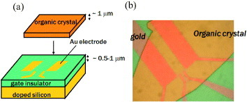
Organic crystal FETs were prepared either by ‘crystal-lamination’ or ‘parylene-coating’ techniques [Citation10–14]. In the former, thin platelets of single crystals, typically less than 1 μ m thick, are grown by physical vapor transport (PVT) and are simply laminated electrostatically on gate-insulating layers. Usually, a few hundred nm thick SiO2 layers [Citation12, Citation13] or polymeric insulators such as poly-4-vinylphenol (PVP) or amorphous fluoropolymers, which are also common in thin-film transistors [Citation37, Citation38], are used for the gate insulators [Citation7, Citation39–41]. Few nm thick gold electrodes are evaporated and patterned by photolithography beforehand, so that the electrical contacts between the semiconductors and the metal are also made by the mere electrostatic bonding. A typical structure of the ‘laminated-crystal’ SC-OFET is illustrated in figure (a), and the top view is given in figure (b).
Figure 1 (a) Illustration of structuring SC-OFETs with the method of crystal lamination. (b) A top view of the SC-OFETs with a thin laminated rubrene crystal.
The SiO2 layers were formed by usual thermal oxidization to a thickness of 500 nm. The PVP gate insulators are prepared as follows: a solution of poly-4-vinylphenol and polymelamine-co-formaldehyde in propylene glycol monomethyl ether acetate (PGMEA) is deposited by spin-coating and is cross-linked at 200 ∘ C for 20 min. With independent measurement of the PVP-film thickness di using a 3D laser microscope, the relative dielectric constant ε i is estimated as ∼4.0 [Citation7]. On the other hand, the technique of forming polymeric gate insulators with parylene was developed to softly coat the surface of the organic molecular single crystals [Citation10, Citation11, Citation14]. For this method, thicker free-standing crystals (typically thicker than 10 μ m) are used. Source and drain electrodes are formed by painting carbon or metallic pastes. Then, a thin film of parylene is deposited to a thickness of ∼1 μ m on top of the crystal in a reactor; the reactor consists of a quartz tube with one closed end and three temperature zones. The dimer para-xylylene vaporizes in the vaporization zone at 100 ∘ C, cleaves in the pyrolysis zone at 700 ∘ C, and polymerizes in the deposition zone, where the samples are located at room temperature and at a pressure of ∼0.1 torr. Finally, gate electrodes are painted on the parylene gate dielectric to cover the region between the source and drain electrodes. Figure (a) shows an illustration of this structure.
Figure 2 (a) SC-OFETs with parylene gate insulating layers. (b) SC-OFETs with vacuum-gap dielectrics.
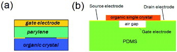
It is to be noted that the key technology for the above two methods to successfully fabricate high-performance SC-OFETs is the minimization of damage to the surface of fragile organic semiconductor crystals during the process of forming the interfaces to gate insulators. Yet another method reported by Sundar et al involved ‘vacuum-gap’ space being utilized for the gate insulating layer. The use of polydimethyl-siloxane elastomer enables such construction as shown in figure (b), so that the ‘interface’ of the rubrene single crystals with the vacuum results in high mobility of 20–30 cm2 Vs−1 at the crystal surface [Citation4, Citation5]. This value is comparable to the mobility reaching 25–40 cm2 Vs−1 reported by Takeya et al for inner crystal channels of rubrene SC-OFETs, measured with very weak gate electric fields [Citation6, Citation7].
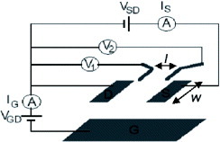
To characterize the intrinsic carrier transport property of the SC-OFETs, four-terminal conductivity measurement can be useful in addition to conventional methods of measuring the drain current ID between two (source and drain) electrodes as functions of drain voltage VD and gate voltage VG, because this can exclude the influence of parasitic contacts [Citation11, Citation12]. Figure shows a schematic of an electrical circuit for measuring ID and gate leakage current IG, by applying VG and VD. By detecting voltages V1 and V2 at two positions on the crystal, longitudinal sheet conductivity σ ϒ=ID /(V2 - V1 )L12 /W is evaluated, where L12 is the distance between the two voltage probes in the current direction and W is the channel width. Mobility μ 4T is estimated from the measured transfer characteristics σ ϒ (VG ) using the formula
1 based on
2 Here p denotes density of the holes, e is the electron charge, Ci is the capacitance of the gate insulator per unit area and Vth represents threshold gate voltage. The more commonly used two-terminal mobility μ 2T can be estimated from the equation
3 where L is the distance between the source and drain electrodes. In addition, saturation mobility μ sat can be estimated when the measurement reaches the saturation regime with VD typically larger than VG - Vth as
4 IsatD represents the saturation current.
Figure 3 Schematic diagram of the four-terminal conductivity measurement with applied gate voltage in OFETs.
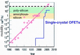
The history of the growth of carrier mobility in OFETs is given in figure . Developing high-mobility OFETs is a key technology for establishing an extensive market for organic electronics in the future, providing easy-to-fabricate switching components in integrated logic circuits. For example, beyond being a candidate for active matrix-controlling elements, organic transistors could be applied to driving-circuit components in all organic display frames, with mobility more than one-order higher than presently achieved. Attempts have been made to maximize transistor mobility by employing organic single crystals as the active semiconductors in order to generate serious consideration of applicability of organic transistors further extended to the material limit and predict the ultimate size of the market in the future.
Figure 4 History of the development of high-mobility OFETs. Red open circles indicate representative values of mobility for certain years.
SC-OFETs of rubrene
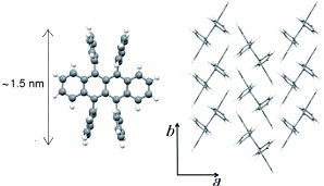
The representative semiconductor material for SC-OFETs is rubrene, whose molecular and crystal structures are shown in figure . Such SC-OFETs were first constructed by Podzorov et al with parylene gate dielectrics [Citation10], after which laminated-crystal OFETs were also developed [Citation15, Citation42]. This compound turned out to be highly compatible with both device structures, resulting in benchmark mobility values in all OFETs [Citation4–7].
Figure 5 Molecular and crystal structures of rubrene.
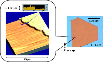
To fabricate SC-OFETs by the lamination technique, platelets of crystals only 1 μ m thick are used. Figure shows an atomic force microscopy (AFM) image of the surface of a rubrene crystal, revealing a remarkably flat surface. The surface quality is apparently important for carrier transport in OFETs because the field-induced carriers are mostly confined to the vicinity of the interfaces to the gate dielectric layers, suggesting that the property is partially responsible for the achieving high mobility.
Figure 6 A molecularly flat surface extends a few tens of micrometers at the surface of rubrene crystals (an AFM image).
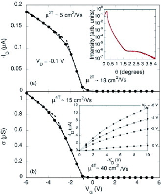
A very high mobility is achieved for devices with self-assembled monolayers (SAMs) coated on SiO2 dielectrics [Citation6]. The surface treatment procedure appears effective in reducing the influence of both defects in SiO2 and the amount of absorbants such as water molecules. Silane self-assembled molecules are carefully attached by chemical vapor deposition. As the result of the mobility estimation, some of the devices exhibit record high values with the application of a weak electric field, as shown in figure . It is discussed that carriers can distribute more into the crystal, so that they are less subject to the random potential at the surface of amorphous SiO2 dielectrics [Citation6, Citation7].
Figure 7 Transfer characteristics of rubrene single-crystal transistors fabricated on SiO2 dielectrics treated with SAMs. (a) and (b) represent the results of two-terminal and four-terminal measurements, respectively. The inset in the upper panel shows low-angle x-ray diffraction of the highly ordered SAMs, while the inset in the lower panel presents output characteristics (reproduced with permission from [Citation6]).
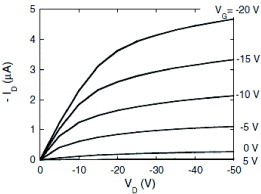
The method of crystal lamination allows the use of any materials of gate insulators for fabrication of SC-OFETs because the crystals are laminated on independently prepared gate dielectric surfaces at room temperature in air. Thus far, various gate dielectric materials other than SiO2 have been tested with rubrene single crystals as the standard material, and most of them showed good transistor performances [Citation43, Citation44]. The materials range from spin-coated polymers such as poly(vinylpyrrolidone) (PVP) [Citation7], fluoropolymer CYTOP (Asahi Glass Co.) [Citation40, Citation41], high-k oxides such as Ta2 O5 [Citation43, Citation45], and even an organic single-crystal insulator [Citation46] and electrolytes such as ionic liquids [Citation47, Citation48]. Hulea et al reported systematic dependence of the mobility on dielectric constants of the gate dielectric materials and proposed the formation of polarons coupled with the polarization of the gate dielectric materials, owing to the additional mass gained in the renormalized quasiparticles as a result of the dressing effect [Citation43]. The fluoropolymer devices are characterized by very small hysteresis with respect to the gate voltage sweep and also by good reproducibility among devices. Typical for this type of device output characteristics are shown in figure with a high saturation mobility of 30 cm2 Vs−1.
Figure 8 Output characteristics of a rubrene SC-OFET with CYTOP gate insulators. Hysteresis is negligible. Saturation mobility is estimated as high as 30 cm2 Vs−1 (reproduced with permission from [Citation40]).
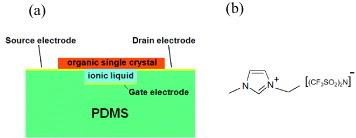
Rubrene SC-OFETs are formed even at solid-to-liquid interfaces with ionic liquids, as reported in [Citation48]. Interest in room-temperature ionic liquids is growing because of the prospect of nonvolatile ‘green solvents’ and owing to the development of chemically stable, water-proof, and nontoxic compounds during the last decade [Citation49]. Such materials have been attractive not only for technologies for the production of chemicals without volatilizing organic solvents, both in industry and chemistry laboratories, but also for applications to energy conversion and energy storage devices, making use of their fast ionic diffusion. The materials are indeed being applied to electrolytes for lithium ion batteries and fuel cells. However, the use of the ionic liquids for electronic devices is not as developed as the above areas. Solid-to-liquid interfaces are formed between organic semiconductor single crystals and ionic liquids, so that the structures work as fast-switching organic field-effect transistors (OFETs) with the highest transconductance, i.e. the most efficient response of the output current to the input voltage, among all OFETs.
Unlike conventional OFETs, the ionic liquid devices enable minimized operational gate voltage: when VG is applied to the ionic liquid layer, the electric double layers are formed as a result of the motion of the ions. Noting that gate electric field is confined only to electric double-layers 1 nm thick, only a fraction of a volt is necessary to accumulate the same carrier density as when 100 V is applied to gate dielectrics more than two orders of magnitude thicker. There have been reports on the use of polymer electrolytes such as LiClO4 dissolved in poly(ethylene oxide) or ionic liquids maintained in a polymer gel [Citation51–55]. However, these devices suffer from either poor mobility or slow response to the applied VG because of relatively slow ionic diffusion in the polymer platforms. The ionic-liquid gel device exhibits the best performance among the electrolyte OFETs, realizing a maximum response frequency of 5 kHz and a mobility up to 1 cm2 Vs−1. To make the best use of ionic conduction in the ionic liquids, a well structure is useful to hold the liquid underneath organic single crystals by capillary force (figure (a)); the structure is formed with a polydimethylsiloxan (PDMS) elastomer on which a rubrene single crystal is electrostatically attached. When a pure ionic liquid of 1-ethyl-3-methylimidazolium bis(trifluoro-methyl-sulfonyl)imid [emimTFSI] (figure (b)) is used, whose ionic conductivity may be as high as 10- 2 S cm- 1, the maximum cutoff frequency is in the MHz range with a well height of 20 μm.
Figure 9 (a) A well structure to hold ionic liquid to form SC-OFETs with solid-to-liquid interfaces. (b) 1-ethyl-3-methylimidazolium bis(trifluoro-methyl-sulfonyl)imide [emim TFSI], as an example of an ionic liquid (reproduced with permission from [Citation49]).
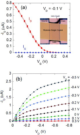
High mobility of the rubrene single crystals and high capacitance of the electric double layer result in the best performance. As shown in figure , the device in figure exhibits high current amplification efficiency with the application of only a fraction of a volt as the gate voltage. The sheet transconductance σ ϒ T, defined by L/W dID /dVG, measures the rate of the current amplification for OFET devices and therefore directly determines the transistor performance. Since σ ϒ T is the product of mobility and the capacitance of the device, both parameters should be large to have the best sheet transconductance. σ ϒ T is as high as 20 μ S when VD = - 1 V, which is the best performance among all reported OFETs [Citation50].
Figure 10 (a) Transfer and (b) output characteristics of the ionic liquid/rubrene SC-OFETs. Inset in (a): optical view of the device (reproduced with permission from [Citation49]).
As has been shown in this section, rubrene has been the standard organic semiconductor material for SC-OFETs. The above-mentioned devices realized the benchmark mobility of organic transistors, and have been and will continue to be a useful platform to study the influence of the gate dielectric.
SC-OFETs of pentacene
Molecular and crystal structures of pentacene, the most popular organic semiconductor, are shown in figure . Pentacene has been the most common material for OFETs since the 1980s; therefore, it is useful to use it for comparison. However, fabrication of pentacene SC-OFETs is far harder than that of rubrene devices that realize similar level of performance. The reason is mostly due to the chemical instability with oxygen in the atmosphere, which easily oxidizes pentacene to pentacene-quinone. In the first report in 2003, a mobility of only 0.5 cm2 Vs−1 was obtained with the crystal lamination technique [Citation12], and the value increased to 3 cm2 Vs−1 afterwards when the surface treatment on the SiO2 gate dielectrics was improved [Citation15].
Figure 11 Molecular and crystal structures of pentacene. ‘Z’ represents the axis perpendicular to the molecular layers.
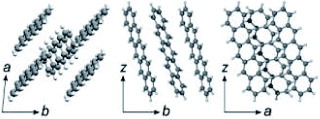
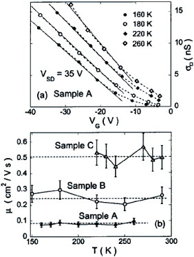
Figure (a) presents electric field induced conductivity σ ϒ as a function of VG at different temperatures from 160 to 260 K [Citation12]. While the temperature dependence is obvious in the low VG region, the maximum slope at high VG does not differ much with changing temperature. For each temperature, the mobility is estimated from the maximum slope, and is plotted in figure (b). The results for two more crystals (samples B and C) are also shown in addition to the one for figure (a). The mobility values range from 0.1 to 0.5 cm2 Vs−1, with no apparent temperature dependence. The mobility values of our devices are also comparable to those of high-quality pentacene thin-film FETs, though they are somewhat lower than the best metal oxide semiconductor (MOS) device. Since it is not likely that such extrinsic mechanisms dominate μ (T) in our four-terminal measurement of single crystals, the nearly temperature independent μ (T), at least from 150 K to near room temperature, appears to be an intrinsic property of the surface of the pentacene single crystals, motivating us to investigate the fundamental intermolecular charge dynamics more quantitatively. The nearly temperature-independent feature is inconsistent with conventional hopping models which predict strong T dependence. A difficulty also arises in the band picture, because of a naive estimation of the mean free path, resulting in a value shorter than the distance between adjacent molecules. Allowing for polaron formation, which is common in dilute-charge systems, the nearly temperature-independent feature is deduced for naphthalene; however, since the calculation is based on a balance between electronic parameters such as bandwidth and phononic parameters, the applicability to the case of pentacene crystals has to be further explored. The combination of a short mean free path and an almost temperature-independent conductivity is reminiscent of the T independent interlayer charge transport near room temperature in a high-Tc cuprate. There, metallic planes are stacked at a subnanometer distance. It is argued that direct tunneling between the adjacent planes dominates the interlayer transport in such systems.
Figure 12 (a) Channel conductivity versus gate voltage at different temperatures from 160 to 260 K. (b) Field-effect mobility as a function of temperature for three different pentacene single-crystal devices (reproduced with permission from [Citation12]).
Jurchescu et al reported that the method of forming pentacene-quinone on pentacene crystals and using it for gate insulating layers results in very high-mobility carrier transport at the interface between pentacene and the quinone layers [Citation8]. The mobility reaches as high as 30–40 cm2 Vs−1, though the estimation includes a certain ambiguity of estimating the thickness of the quinone layers. The structure is reminiscent of a silicon MOSFET, which contains a high-quality interface between single-crystal silicon and its oxide layer, thereby realizing high-mobility carrier transport and high-performance transistor functions.
SC-OFETs of TTF analogues
Tetrathiafulvalene (TTF) and its analogues are known as the most important components of highly conductive organic charge-transfer compounds [Citation56]. It is expected that their ability to afford a vast variety of molecular conductors and superconductors permits their use in high-performance single-component channel materials of OFETs. To date, organic thin-film transistors with a mobility of about 0.1–1.4 cm2 Vs−1 have been reported for some TTF analogues [Citation57–63]. Figure (a) shows the molecular structures of some TTF analogues studied for OFETs: dithiophene-tetrathiafulvalene (DTTTF), hexamethylene-tetrathiafulvalene (HMTTF), dibenzo-tetrathiafulvalene (DBTTF) and dinaphtho-tetrathiafulvalene (DNTTF). It was pointed out that the higher solubility of these materials should be advantageous for their use in low-cost solution processing [Citation57]. In fact, SC-OFETs were fabricated by solution processing for some kinds of TTF analogues [Citation64–67].
Figure 13 (a) Molecular structures of some TTF analogues studied for OFETs; (b) and (c) crystal structures of hexamethylenetetrathiafulvalene (HMTTF). Molecules at different positions along the b-axis are shown in different colors (reproduced with permission from [Citation67]).
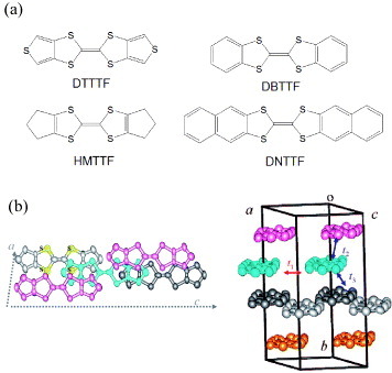
It was recently reported that SC-OFETs based on solution-grown as well as vapor-transport-grown HMTTF single crystals exhibit high mobility exceeding 10 cm2 Vs−1 [Citation67]. Both solution-grown and vapor-transport-grown crystals yield identical monoclinic crystal structures whose packing motif is shown in figure (b). An intermolecular lateral arrangement along the a-axis affords large π –π interactions with close S–S contacts of 3.545(3)–3.647(3) Å. On the other hand, molecules are stacked along the b-axis in a brickwork arrangement in which molecules slip by half their length along the molecular long axes. These structural features are in sharp contrast to the herringbone molecular arrangement of polyacenes like rubrene or pentacene.
The HMTTF SC-OFETs were fabricated with parylene C gate dielectric layers. Thermally evaporated Au, Ag, or TTF–TCNQ metallic thin films on top of the crystals were used as the source/drain electrodes. Figure shows transfer characteristics of the devices measured with a source/drain current along the a-axes. The mobility reached 11.2 cm2 Vs−1 in vapor-transport grown crystals and 10.4 cm2 Vs−1 in solution-grown crystals. It is noted that the output characteristics shown in the inset present the sign of current saturation at high VD, if we assume the additional bulk current in the current–voltage characteristics. This performance could be attributed to the close lateral and brickwork molecular packing, shown in figure (b). Transfer integrals were estimated by extended Hückel molecular orbital calculations, and it was found that the transfer integral is highest (0.1151 eV) along the lateral intermolecular contact (‘t1’ in figure (b)). Here it is noted that the use of TTF-TCNQ organic metal electrodes is essential to achieve a high performance with HMTTF SC-OFETs. As we discuss in subsection 3.1, carrier injections are optimized with TTF-TCNQ organic metal electrodes in TTF analogues.
Figure 14 Transfer and output (inset) characteristics of SC-OFETs composed of single crystals grown by (a) vapor transport and (b) recrystallization (reproduced with permission from [Citation67]).
In the comparison of vapor-transported and solution-processed SC-OFETs, some different features in the device characteristics are observed. A ‘normally on’ state with Vth at 13 V and a high on/off ratio (∼600) is observed in the device containing vapor-transported crystals, whereas a ‘normally off’ state with Vth at about - 6 V and a much lower on/off ratio (<3) is seen in the device containing solution-processed crystals. These different features indicate the relationship between processing and device characteristics in OFETs. The vapor-transport-grown crystals could include a larger number of bulk carriers inside the crystals, possibly associated with thermal decomposition during crystal growth at relatively high temperature. Bulk carriers could be depleted by the reverse gate biases. This may provide the origin of the ‘normally on’ behavior in the transfer characteristics and low off current at high positive voltages. In contrast, the larger off-current in the solution-processed crystals may be associated with conductive paths remaining during the drying process just after the recrystallization from solution.
Air-stable n-type SC-OFETs of TCNQ and PTCDA
High-performance and air-stable OFETs of both p- and n-types are indispensable for extensive applications to organic logic circuits. In particular, it is yet unclear how to build high-performance n-type OFETs with stable operation in air. Reports on such devices are still very limited [Citation46, Citation68]. Compared with p-type devices, air-stable n-type OFETs suffer from either low carrier mobility or very large threshold gate voltages, which are fatal for application to low-power complementary logic devices.
One reason for the poorer performances in the n-type OFETs is argued to be energy-level mismatch between their Fermi levels and the lowest unoccupied molecular orbital (LUMO) levels of organic semiconductors. This causes inefficient electron injection from noble metal electrodes. Moreover, there are also concerns about the interfaces to the gate insulators where the atmospheric oxidants O2 and H2O, absorbed at grain boundaries of organic semiconductors, or OH groups at the surface of SiO2 may also harm electron transport acting as electron-trapping centers [Citation69]. Therefore, SC-OFETs based on n-type organic single crystals have been developed for more fundamental evaluation of intrinsic device properties, eliminating influences of grain boundaries and film morphology, as have been studied for p-type single-crystal OFETs.
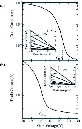
The air-stable n-type single crystal transistors of TCNQ and PTCDA are successfully fabricated by crystal lamination. Au electrodes are used as usual. Figure shows an optical-microscope view of a TCNQ single-crystal transistor. Because of the high electron-affinity of TCNQ, the reported LUMO levels (∼4.8 eV lower than vacuum level) are close to the work function of Au electrodes (∼5.1 eV) [Citation70]. The transfer and output characteristics of one of the prepared TCNQ single-crystal transistors are shown in figure . All five devices exhibit textbook like n-type transistor performance with negligible hysteresis and negligible threshold. Linear-region mobility was calculated using the standard formula as 0.05–0.3 cm2 Vs−1 and 0.2–0.5 cm2 Vs−1 from transfer curves of two-terminal measurements shown in figure (a) and from the evolution of the four-terminal conductivity σ 4T shown in figure (b). Also, as the output performance exhibits typical saturation behavior shown in figure (c), saturation mobility is deduced as 0.2–0.5 cm2 Vs−1. These values are three orders of magnitude higher than those of TCNQ thin-film transistors [Citation71], indicating that the intrinsic material performance of n-type OFETs was not realized in previous experiments with polycrystalline films, presumably because of such extrinsic influence as of grain boundaries.
Figure 15 Left: optical view of the TCNQ SC-OTFET. Right: molecular and crystal structures of TCNQ (reproduced with permission from [Citation46]).
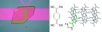
Figure 16 Transfer characteristics of typical TCNQ SC-OFETs measured with (a) two-terminal and (b) four-terminal methods. (c) Output characteristics of the TCNQ transistor (reproduced with permission from [Citation46]).
It is to be emphasized that the threshold voltage Vth is negligible in the present TCNQ single-crystal transistors, indicating absence of effective deep trap levels at the interfaces between the single-crystal surfaces and the SiO2 gate insulators. The result contrasts with the fact that the majority of organic transistors suffer from significant or fatal effects of deep electron traps, causing poor performance of the n-type transistors. As a result of tremendous effort in developing n-channel semiconductors, air-stable and high-mobility devices were reported recently [Citation68, Citation72, Citation73]. However, reports on transistors with a Vth less than 10 V are very rare and poorly reproducible. To further understand the mechanism of minimizing the threshold, we use other similarly prepared single-crystal transistors for comparison.
As another example of air-stable n-type OFETs, poorer performance of PTCDA single-crystal transistors is reported; a typical mobility value is only ∼10−3 cm2 Vs−1, and Vth is typically as high as 30–50 V [Citation31]. Since the LUMO level of PTCDA is ∼3.9 eV lower than the vacuum level, which is ∼1 eV higher than that of TCNQ, it can be argued that PTCDA devices suffer from more severe barriers for electron injection, if one neglects energy-level renormalization at the interfaces due to such influences as from interface dipoles. We also note that similarly prepared single-crystal transistors based on rubrene, which has an even lower LUMO level of ∼3.2 eV from the vacuum level, never work as n-type transistors in air.
In addition to the argument about electron-injection barriers at the gold-semiconductor interfaces, often concerned is the effect of deep traps at the boundary to the gate insulators. Since the effects of OH and water-based reactions are of particularly concern, we also prepared TCNQ single-crystal devices with highly water-repellent amorphous fluoropolymer gate dielectrics which do not possess OH groups [Citation72, Citation73]. The exhibited transistor characteristics were almost identical to those of the SiO2 devices, indicating the minor effects of electron-trapping centers. The advantages of possessing high electron affinity are not only in lowering electron-injection barriers from noble-metal electrodes. More importantly, oxidizing components, such as OH groups and water which are often concerned as electron-trapping centers, are inactivated because the LUMO levels of the semiconductor channels attract electrons more effectively. Therefore, the experiments tell us that intrinsic material properties of organic compounds with high electron affinity suffice high-performance and air-stable n-type transistors indispensable for low-loss organic complementary circuits.
SC-OFETs of charge-transfer compounds
Charge-transfer compounds are binary systems composed of electron-donor (D) and electron-acceptor (A) molecules or those with inorganic counterparts [Citation56]. These compounds are well known to provide a wide spectrum of metallic materials, including more than 100 kinds of organic superconductors. Most representative components are TTF-based donor molecules as presented in subsection 2.4, and TCNQ-based acceptor molecules as presented in subsection 2.5. Figure shows an example: ‘mixed-stack’ charge-transfer compounds of DBTTF-TCNQ are composed of alternate stacks of DBTTF donors and TCNQ acceptors along the b-axis [Citation74]. A fundamental feature of the charge-transfer compounds is that the intermolecular charge-transfer interaction, or intermolecular charge resonance, binds D and A molecules much more tightly than the van der Waals interaction. The compounds afford a rich variety of narrow-gap molecular semiconductors. Owing to the strong charge-transfer interaction, the band width in such molecular semiconductors is larger than that in single-component molecular materials. Here, we present some examples of SC-OFETs using prototypical semiconducting charge-transfer compounds as channel single crystals.
Figure 17 Molecular and crystal structure of a (DBTTF) (TCNQ) charge-transfer compound.
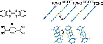
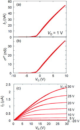
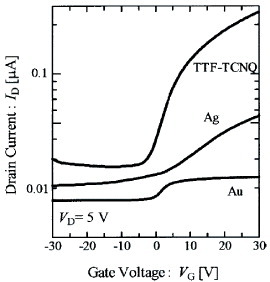
DBTTF-TCNQ, as presented in figure , is composed of D and A molecules with nominally neutral valence states. The semiconducting gap is ascribed to the charge-transfer excitation from the HOMO (highest occupied molecular orbital) band of DBTTF to the LUMO (lowest unoccupied molecular orbital) band of TCNQ along the mixed stacks. From the infrared absorption spectra, the charge-transfer degree from DBTTF to TCNQ is found to be about 0.46, and the optical gap is estimated as 0.9 eV. Figure shows transfer characteristics of SC-OFETs using DBTTF-TCNQ as channel single crystals. In the fabrication of field-effect devices, parylene C was used to form a gate dielectric layer with a typical thickness of about 1.0 μ m (Ci = 2.12 nF cm- 2). Three kinds of metallic thin films using TTF–TCNQ, Ag and Au are used, respectively, as source/drain electrodes in the devices. Among them, n-type mobility of about 1.0 cm2 Vs−1 is obtained with TTF-TCNQ electrodes. In the device with TTF-TCNQ electrodes, electron injections are optimized from electrodes to the channel crystals, as discussed in the next section.
Figure 18 Transfer characteristics of DBTTF-TCNQ SC-OFETs with the source and drain electrodes composed of Au, Ag and TTF-TCNQ, measured along the b-axes (reproduced with permission from [Citation16]).
The charge-transfer compounds are also known to afford a variety of functional molecular semiconductors whose gaps result from strong electron–electron or electron–phonon interactions. Field-effect doping in such materials is of particular interest in condensed matter physics. Ambipolar-type field-effect characteristics are observed in SC-OFETs using Mott insulators of (BEDT-TTF)(F2
TCNQ) [BEDT-TTF (] [Citation14], and of (BEDT-TTF)(TCNQ) [Citation75] as channel single crystals. The unique ambipolar operations may be associated with the effect of carrier accumulation at the Schottky barriers in the source/drain contacts with Mott insulators [Citation76, Citation77]. Kawasugi et al have also recently reported field-effect-transistor operations in the semiconducting phase in the vicinity of the superconducting phase in κ-(BEDT-TTF)2Cu[N(CN)2 ]Br [Citation30].
Physics of SC-OFETs
Charge injections
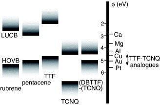
As discussed in subsection 2.1, SC-OFETs are conventionally fabricated using single crystals of undoped (or ‘intrinsic’) molecular semiconductors where the electrical contacts are formed directly with inorganic metals. This is significantly different from the contacts in typical silicon-based semiconductor devices, in which doping is conventionally utilized to enhance the tunneling efficiency as well as to control p- and n-type carrier injections. Such simple metal/semiconductor contacts are possible in SC-OFETs, since interfacial states are not as serious as in inorganic devices owing to the weak nature of van der Waals intermolecular interactions. Figure shows a band diagram for the lowest unoccupied conduction band (LUCB) and the highest occupied valence band (HOVB) of some of the molecular semiconductors presented in subsections 2.2–2.5. This figure also includes work functions of various inorganic and organic metals. The starting point for the consideration of the carrier injections is the Mott–Schottky vacuum level alignment for these energy levels at the metal/semiconductor contacts. We must then consider other factors, for example, the formation of a Schottky barrier or an interfacial dipole layer, in case appreciable contact resistance is observed [Citation78].
Figure 19 Schematic band diagram for lowest unoccupied conduction band (LUCB) and highest occupied valence band (HOVB) of various molecular semiconductors and the work function of inorganic and organic metals.
To discriminate the contact resistance from the resistance of conducting channels, four-terminal conductivity measurement was utilized in some SC-OFETs [Citation11, Citation12, Citation15]. The method is quite useful to extract the intrinsic charge-carrier mobility, as discussed in subsection 2.1. Usually the source contact resistance decreases slightly with increasing drain voltage. The behavior is consistent with the Schottky-like barrier formation at metal/semiconductor contacts. Such a dependence of mobility on VD demonstrates the importance of contacts for a small VD.
From the fundamental viewpoint of charge transport in intrinsic semiconductors, SC-OFETs could support both electron and hole conductions. However, electron and hole injections into molecular semiconductors are restricted owing to the energy difference between semiconducting band states and work functions of electrode materials, as shown in figure . An appropriate choice of electrode materials is necessary to optimize carrier injections in terms of appropriate work functions, which should be close to the HOVB or LUCB for efficient hole or electron injections, respectively. It has been recently reported that pentacene and tetracene allow for good electron injections from low-work-function metals like calcium and exhibit n-type FET operation [Citation79]. The topic has now been studied in conjunction with organic light-emitting field-effect transistors (OLETs), a novel class of organic multi functional devices [Citation21, Citation25, Citation29, Citation79]. For the operation of OLETs, both p- and n-type carrier injections are necessary for electron-hole recombination in the channels. Studies have shown that electron transport in SC-OFETs is sensitive to air. To observe n-type FET operation, devices are fabricated without exposure to air to prevent the formation of electron traps.
Achieving tunability in carrier injections is a fundamental issue in organic electronics. It is suggested that metallic molecular donor–acceptor compounds are useful for controlling carrier injections at metal/semiconductor contacts; this suggestion is related to the chemical tunability of organic molecules [Citation16, Citation19]. For example, the electron affinity of component TCNQ molecules can be modified by fluorine substitutions to form Fn TCNQ (n= 1, 2, 4). Since the metal Fermi energy of metallic molecular donor–acceptor compounds is located in the midst of the HOMO levels of donors and LUMO levels of acceptors, chemical tunability allows fine control of the metal Fermi energy of metallic molecular donor–acceptor compounds. It was demonstrated, with use of prototypical SC-OFETs, that p- and n-type operations can be successfully controlled by tuning the Fermi energy in metallic molecular donor–acceptor compounds [Citation19]. Here, we discuss the nature of carrier injections at such organic metal/organic semiconductor interfaces.
In the experiment, three kinds of organic donors (D: TTF, TSF = tetraselenafulvalene, and DBTTF) and four kinds of organic acceptors (A: TCNQ, F1 TCNQ, F2 TCNQ and F4 TCNQ) were employed to produce conductive charge-transfer complex films as the electrodes. Single crystals of the semiconducting mixed-stack charge-transfer compound DBTTF-TCNQ, as presented in subsection 2.6, are utilized as channel semiconductors. As presented in figure , the device with TTF-TCNQ electrodes shows large field-effect response compared with Ag or Au electrodes. The measured transfer characteristics are presented in figure for devices with six kinds of organic metals as source and drain electrodes. Clearly, the n-type behavior with (a) TTF-TCNQ electrodes changes to ambipolar-type for (c) and (d), and then to p-type for (e) and (f). The results can be explained in terms of the variation of the metal Fermi energy with respect to the semiconductor band energy. The Fermi energy can be chemically controlled over the range from the conduction band edge to the valence band edge of the DBTTF-TCNQ channel.
Figure 20 Transfer characteristics at VD = 5 V of DBTTF-TCNQ single-crystal field effect transistors with source and drain electrodes composed of (a) TTF-TCNQ, (b) TTF-F1 TCNQ, (c) TTF-F2 TCNQ, (d) TSF-F1 TCNQ, (e) TSF-F2 TCNQ and (f) DBTTF-F4 TCNQ measured along the crystal long axes (reproduced with permission from [Citation19]).
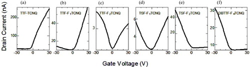
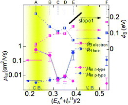
In terms of the relative size of the field-effect response, a much larger enhancement was observed in the unipolar devices ((a), (e) and (f)) than that in the ambipolar ones ((c) and (d)). For comparison, the values μlin =|dID /dUG|× (L/WCiVD ) are plotted in figure for both p- and n-type field-effect responses. Nominal mobility values are plotted since the channel mobility should fundamentally be the same for all devices. Instead, the distinct variation of μ lin is associated with the change in the injection efficiency at the metal/semiconductor contacts. From the temperature dependence of the transfer characteristics, the mobility is determined by the thermionic emission, i.e. thermally activated charge hopping against the Schottky barriers, φ B, above 200 K. The upper part of figure shows the Schottky barrier height of all the devices. Clearly, the slope, S= dφ B /dφ m, is roughly equal to unity for both p- and n-type carrier injections for devices (a)–(e) shown in figure . This result implies that both electron and hole injections can be understood in terms of the Mott–Schottky rule, in which the vacuum level alignment rule basically holds for Schottky barrier formation. These features indicate that the organic metal/semiconductor contacts can form weakly interacting ideal interfaces, free of interface states in the band gaps.
Figure 21 Schottky barrier characteristics at organic metal/semiconductor contacts. Linear (left ordinate) and Schottky barrier height (right ordinate) plotted against (IPD+EAA)/2 (fm) of the organic metals used as source and drain electrodes (reproduced with permission from [Citation19]).
Hall effect and intrinsic transport of field-induced carriers
One of the important products of developing high-mobility SC-OFETs has been successful Hall-effect measurements, independently reported in 2005 almost at the same time [Citation33, Citation34]. As a result, it is evidenced that band transport is indeed realized for the carriers generated at organic semiconductor crystals with highly overlapped orbitals between adjacent molecules. Note that Hall-effect measurement later became possible also for pentacene thin-film transistors, showing that the accumulated carriers are nearly band-like [Citation80].
Doped π-conjugated molecular semiconductors basically provide unique electronic systems with a relatively small intermolecular transfer integral (typically ∼0.5 eV) and significant coupling to molecular vibration, both of which play a major role even at ordinary temperatures. Simply, the two fundamental transport mechanisms would be a band transport with mass-enhanced carriers and a hopping transport with self-localized carriers in predominance of molecular reorganization energy [Citation1]. In reality, however, there is a complex competition between the two extreme cases, grounded on experimental and theoretical works introducing the idea of ‘polaronic band transport’ [Citation81–84]. Though understanding the carrier transport in such ‘soft’ semiconductor crystals is of emergent importance because of recent technological attention to organic flexible electronics, methods of experimental approaches are still under development toward a full description of the fundamental electronic states of the charge carriers, which provided significant motivation for the Hall-effect measurements.
One of the first samples for the measurements were SC-OFETs with laminated thin rubrene crystals on PVP/doped silicon substrates. The samples are further shaped for the Hall-effect measurements into the ‘six-probe Hall-bar’ using laser etching [Citation85]. Measurement of the transverse Hall voltage VH require evaluating voltages at three points on the crystal; V1, V2 and V3 as presented in figure (d), using additional source measure units (SMU). It yields longitudinal sheet conductivity σ ϒ and VH =V3−V1 in external magnetic field B perpendicular to the channel.
Figure 22 (a) Transfer characteristics of a rubrene single-crystal field-effect transistor at 290 K. The inset is a top view of the device. (b) Evolution of transverse voltage in a Hall bar shaped rubrene single-crystal field-effect transistor at 290 K for four different gate voltages from 25 to −175 V. The magnetic field is swept back and forth between −10 and 10 T perpendicular to the conduction channel, as shown in (c). (d) Inverse Hall coefficient and sheet conductivity plotted as a function of gate voltage at 290 K for the Hall bar shaped rubrene SC-OFETs illustrated in the inset. (e) Hall mobility as a function of gate voltage. The solid curve indicates a typical estimation of carrier-distribution depth in units of the c-axis lattice constant of rubrene. The dashed line shows the two-monolayer criterion as a guide [Citation7].
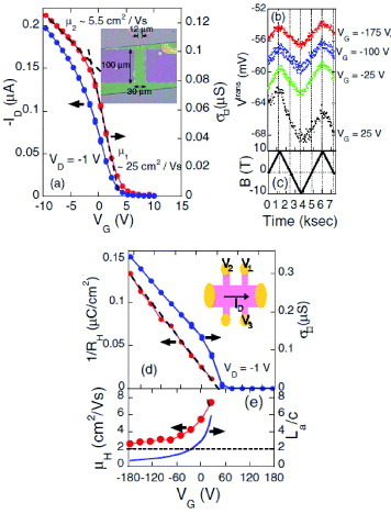
Prior to the Hall-effect measurements, we characterized the device by usual longitudinal conductivity measurements in zero magnetic field. Plotted in the main panel of figure (a) is drain current ID as a function of VG in the ohmic regime. It is a general trend that transconductance is larger for VG near Vth than at higher negative VG. The mobility value is evaluated as 5–25 cm2 Vs−1 near Vth, while it is ∼1–2 cm2 Vs−1 at large negative gate voltages, depending on the samples.
For the Hall-effect measurement, an external magnetic field is slowly swept between 10 and - 10 T back and forth to extract the field-dependent component from the evolution of transverse voltage Vtrans. Figure (b) shows Vtrans as a function of time in magnetic field B, which change as figure (c). Subtracting slightly drifting components by linear approximation, the Hall coefficient RH is derived as RH = ΔVH /ID ΔB. The sign of RH is positive, which is consistent with the hole accumulation in the rubrene crystals. The inverse of the Hall coefficient is plotted in figure (d) together with σ ϒ as a function of gate voltage. In contrast to the nonlinear profile of σ ϒ (VG ), 1/RH increases linearly for VG <Vth. Moreover, the line of Ci (VG <Vth ), which shows the amount of charge modulated by VG, agrees well with the 1/RH (VG ) profile. Here Ci is capacitance of the gate insulator. The result means that 1/RH is indeed a good measure of the number of carriers in the rubrene crystal, demonstrating extended electronic states that manifest themselves in significant wave function overlap. In addition, the linear increase of 1/RH with VG indicates an absence of anomalous polarization of the gate dielectric layer. Therefore, the change in the slopes of the transfer curves is solely due to the significant VG dependence of σ ϒ. Hall mobility μ H estimated by RH σ ϒ gives the average mobility of mobile carriers and is argued to give an intrinsic carrier mobility excluding the influence of trapping events. μ H is plotted as a function of VG in figure (e), showing that μ H decreases rapidly with the negative VG. The result demonstrates nonequivalence of carriers introduced under different gate electric fields; neglecting electron correlation in such a low-carrier-density system, the μ H (VG ) profile comes from variation of the mobility values depending on the spatial distribution of the carriers. Under high gate fields, the carriers are localized at the interface because of a larger attractive electrostatic force and a shorter screening length. Therefore, the result of figure (e) indicates that μ H of the carriers located near the interface is reduced by significant scattering subjected to random potential on the amorphous polymers. On the other hand, carriers are more spread into the inner crystal because of more pronounced thermal diffusion against weaker gate fields. Since diffusive band-like transport is assumed in the above mechanism, we examine whether the mean free path l can be sufficiently long with the maximum mobility of ∼8 cm2 Vs−1 in figure (e). Within the nondegenerate electron gas model, l can be evaluated at least ∼0.75 nm at 300 K, assuming the effective mass of the holes m to be more than twice as large as the free electron mass. As compared with the intermolecular distance b(∼0.37 nm) in the stacking direction, l is more than a few times longer, leaving a room to be reduced by additional scattering. When μH decreases down to ∼2.5 cm2 Vs−1 at higher gate voltage, the above simplified calculation gives l comparable to b, so that the picture of the diffusive model becomes marginal.
To have more microscopic ideas, one can employ a simple argument of the competition between (i) the gate electric field to confine the carriers to the interface and (ii) their tendency to thermally diffuse into the crystal. A length scale La is introduced for the carrier distribution in the direction of thickness in the organic crystal, based on the Poisson’s equation as discussed in [Citation86]. La can be given as ∼2εs kBT/[eCi(VG - Vth )], where ε s, kB and T are the dielectric constant of rubrene in the thickness direction, the Boltzmann constant and temperature, respectively. Assuming that ε s ∼3ε 0 (ε 0 is the dielectric constant in vacuum) and that Vth ∼50 V, La is estimated for each VG as shown in figure (e) in the unit of the lattice constant c in the thickness direction. Since μ H drastically varies as VG with the carrier distribution of a-few-monolayer thicknesses, the μ H (VG ) profile in figure (e) can be viewed as a crossover from in-crystal to surface (a few monolayer) carrier transport in the rubrene crystals. Therefore, the above simple estimation of La appears consistent with the present experiment, though more precise evaluation is needed to define the exact crossover point avoiding ambiguities in Vth and the residual interface charge.
Microscopic study by ESR
One of the difficulties in revealing microscopic charge transport in OFETs originates in the small number of accumulated charges at channel/gate dielectric interfaces. This prevents us from applying a variety of microscopic measurements used for bulk materials. It is crucially important to find out a possible experimental method to investigate microscopic states of conduction as well as localized carriers in channel semiconducting materials. Recently, it has been demonstrated that field-induced electron spin resonance (FI-ESR; ESR induced by gate electric field) is a powerful method to investigate charge transport in OFETs [Citation35, Citation36]. Here we discuss methods and results of FI-ESR, mainly on the results for pentacene TFTs. It is also shown that the method is applicable in rubrene SC-OFETs.
ESR spectroscopy is a method to detect magnetic resonance absorption of microwaves by Zeeman splitting of electron spins [Citation87]. It is possible to discuss the dynamic as well as the static nature of charge carriers that possess spin moments by analyzing the ESR spectral line shapes and widths. Sensitive measurements are possible, especially in organic materials, since the materials are composed of light elements and show sharp ESR absorption spectra associated with small spin-orbit interactions [Citation88]. Observation of FI-ESR signals was first reported for relatively low mobility OFETs, for which temperature-independent Gaussian-type FI-ESR spectra were obtained and discussed [Citation35]. A subsequent report used relatively high-mobility pentacene TFTs, where the effect of motional narrowing was clearly confirmed with gate-field-dependent and temperature-dependent single-Lorentz-type FI-ESR spectra [Citation36]. The observation of motional narrowing enables us to characterize the movements of charge carriers along semiconductor/insulator interfaces.
Figure (a) shows the scheme for high-sensitive FI-ESR measurements of relatively high-mobility pentacene TFTs with large-area semiconducting channel layers (2.5×20 mm2). Poly(ethylene naphthalate) (PEN) films and high-quality parylene C films were used as nonmagnetic substrates and gate dielectric layers (capacitance of 4.5 nF cm−2), respectively. In the devices, a high density of carriers up to 7 × 1012 cm−2 can be accumulated at the channel/insulator interfaces without electrical breakdown. The channel is composed of vacuum-deposited polycrystalline pentacene films with a grain size of about 200–600 nm. The field-effect mobility is estimated as 0.6 cm2 Vs−1 at VG =−200 V.
Figure 23 (a) Device structures for FI-ESR measurements. (b) Typical FI-ESR spectra of pentacene thin-film transistors (VG = - 200 V) at room temperature. (c) Temperature dependence (Arrhenius plot) of the linewidth ΔB1/2 of FI-ESR spectra at VG = - 200 V and - 100 V, and the field-effect mobility of pentacene thin-film transistors [Citation36].
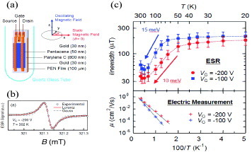
In the devices, the FI-ESR signal is detected only after application of a negative VG. No ESR signal is detected at a positive gate bias. In addition, the spin number estimated from the FI-ESR signal agrees well with the number of charge carriers calculated from the gate capacitance. The features provide clear evidence that the observed FI-ESR signals originate from the field-induced carriers. Figure (b) shows typical FI-ESR spectra at VG = - 200 V. The spectra agree well with first derivatives of single Lorentzian curves over the entire range of measured VG values and temperatures. The linewidth ΔB1/2, defined as the half width at half maximum (HWHM), is as small as 30 μ T at 200 K. It broadens as the temperature decreases in the range 200–50 K, as shown in figure (c). Such temperature dependence gives clear evidence of the motional narrowing effect: resonance spectrum becomes narrower due to the motion of holes because they perceive averaged magnetic field as they move. The increase of ESR linewidth with decreasing temperature indicates that thermal carrier motion is deactivated at lower temperatures, which then suppresses the narrowing effect. In fact, field-effect mobility decreases as the temperature decreases, as presented in the lower panel of figure (c). Figure (c) also indicates saturation of ΔB1/2 at about 180 μ T below 50 K. Continuous wave saturation experiments reveal inhomogeneous broadening of the FI-ESR spectra at temperatures below 50 K, where the motional narrowing may no longer be effective. In contrast, the spectra become more homogeneous at temperatures above 50 K, which is consistent with the motional narrowing effects.
From the motional narrowing theory, the average residence time of carriers at respective sites can be estimated by the following equation [Citation89]:
5 Here, γ is the gyromagnetic ratio, ΔBinhomo is the inhomogeneity of the local magnetic field at respective sites, and τ C is the autocorrelation time of the Larmor frequency. ΔBinhomo could be regarded as the saturated linewidth of about 180 μ T at low temperature, rather than the inhomogeneous linewidth of 500 μ T for isolated pentacene cations as measured in solution [Citation90]. The difference in the hyperfine broadening could be ascribed to the extension of localized electronic states over several molecules in the films. It is also interesting that the saturated value is roughly the same as the temperature-independent linewidth reported for the low-mobility device [Citation35]. This means that the motional narrowing effect is not effective in low-mobility devices even at room temperature, and also that the hyperfine broadening should be common for pentacene films. Using the value of ΔBinhomo = 180 μ T, the τ C can be estimated as about 4 ns at VG = - 200 V at room temperature.
If we assume trap-free band transport, the residence time for each molecule is around 1 ps–10 fs from the calculated bandwidth (∼0.3 eV) for pentacene layers. It is clear that the estimated value for τ C is much larger than the expectation. It is reasonable to attribute τ C to the residence time at shallow or deep traps within the channels. Then, the average traveling length d between the traps can be simply estimated by diffusion theory as 100 nm using the mobility value of 0.6 cm2 Vs−1 [Citation91]. These results agree well with the picture for multiple trap-and-release (MTR) transport in OFETs — the average time at traps is much longer than that for traveling from trap to trap [Citation86]. We may conclude that the observation of the motional narrowing effect in the FI-ESR spectra should give direct evidence for trap-dominated conduction along channel/insulator interfaces.
Within the channels, carriers should be activated to the band states by thermal energy at an average interval of about 4 ns and move from one trap site to another at a relatively high speed, as schematically shown in figure (a). From the Arrhenius plot of ESR linewidth shown in figure (c), we estimated average shallow trap depths of about 10–15 meV, depending on the gate voltages. On the other hand, the activation energy of field-effect mobility is larger, estimated as 62 meV at VG = - 200 V [Citation92]. These features indicate that intragrain charge transport is limited by shallow traps with trap energies of about 10–15 meV, while the charge transport between the source and drain electrodes is strongly affected by areas with a small number of carriers such as Schottky barriers at the source–drain contacts or grain boundaries.
Figure 24 (a) Schematic picture of multiple trap and release (MTR) processes in a pentacene crystal. (b) Gate-voltage-dependence of ESR linewidth (HWHM) of rubrene SC-OFETs at room temperature.
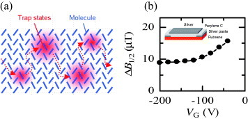
FI-ESR signals with single Lorentzian lineshape are also observed in rubrene SC-OFETs [Citation93–95]. Figure (b) shows the dependence of ESR linewidth of rubrene SC-OFETs on VG at room temperature [Citation93, Citation94]. The ESR linewidth monotonically decreases at low (i.e. low carrier density) and appears to converge at a specific value at high
. Very similar dependence of ESR linewidth on VG is also observed for pentacene TFTs [Citation36]. This feature indicates that deep traps with longer residence times should be filled at low carrier density at low
, and that the portion of shallow traps with shorter residence times gradually increases with increasing
. This means that charge transport is still described by trap-and-release processes in SC-OFETs and is consistent with the activated temperature dependence of carrier mobility in SC-OFETs.
Perspective
High-quality single crystals are prerequisites for the development of silicon-based semiconductor devices, in which homogeneous and well-defined structures are required to characterize and theoretically describe the materials, interfaces and devices [Citation96]. As exemplified in this review, the use of SC-OFETs gives us a new insight into the potential of organic electronic devices. It is demonstrated that the SC-OFETs are useful to evaluate the upper limit of the mobility of materials as well as for gaining a better understanding of the underlying device physics. Although the benchmark carrier mobility of 20–40 cm2 Vs−1 is achieved with rubrene SC-OFETs, it is also found that this performance might still be below the ultimate limit of organic materials owing to the charge trap mechanism in the channel crystals. It is also noteworthy that these findings are based on extremely facile handling techniques used to prepare fairly clean interfaces between molecular single crystals and gate insulating layers. Although the direct use of the SC-OFETs may be incompatible with ‘plastic electronics’ with their target of simple, flexible, and most of all cost-efficient fabrication, commercial success will clearly depend on continuing scientific progress in the understanding of the interface charge transport of π-conjugated organic semiconducting materials using SC-OFETs.
Acknowledgments
The authors thank T Uemura, K Yamada, Y Takahashi and H Matsui for collaboration and discussions on most of the issues focused on in this review. This study was partially supported by a Grant-in-Aid for Scientific Research ‘Molecular Conductors’ (No. 15073201, 2003–2008) by the Ministry of Education, Culture, Sports, Science and Technology of Japan.
References
- PopeMSwenbergC 1999 Electronic Processes in Organic Crystals and Polymers 2nd edn London Oxford University Press
- KlaukH 2006 Organic Electronics: Materials, Manufacturing, and Applications Weinheim, Germany Wiley-VCH Verlag GmbH
- BaoZLocklinJ 2007 Organic Field-Effect Transistors: Optical Science and Engineering Series London CRC Press
- MenardEPodzorovVHurS-HGaurAGershensonM ERogersJ A 2004 Adv. Mater. 16 2097 http://dx.doi.org/10.1002/adma.200401017
- SundarV CZaumseilJPodzorovVMenardEWillettR LSomeyaTGershensonM ERogersJ A 2004 Science 303 1644 http://dx.doi.org/10.1126/science.1094196
- TakeyaJYamagishiMTominariYHiraharaRNakazawaYNishikawaTKawaseTShimodaTOgawaS 2007 Appl. Phys. Lett. 90 102120 http://dx.doi.org/10.1063/1.2711393
- TakeyaJ et al 2007 Phys. Rev. Lett. 98 196804 http://dx.doi.org/10.1103/PhysRevLett.98.196804
- JurchescuO DPopinciucMvan WeesB JPalstraT T M 2007 Adv. Mater. 19 688 http://dx.doi.org/10.1002/adma.200600929
- BrisenoA LMannsfeldS C BLingM MLiuSTsengR JReeseCRobertsM EYangYWudlFBaoZ 2006 Nature 444 913 http://dx.doi.org/10.1038/nature05427
- PodzorovVPudalovV MGershensonM E 2003 Appl. Phys. Lett. 82 1739 http://dx.doi.org/10.1063/1.1560869
- PodzorovVSysoevS ELoginovaEPudalovV MGershensonM E 2003 Appl. Phys. Lett. 83 3504 http://dx.doi.org/10.1063/1.1622799
- TakeyaJGoldmannCHaasSPernstichK PKettererBBatloggB 2003 J. Appl. Phys. 94 5800 http://dx.doi.org/10.1063/1.1618919
- de BoerR W IKlapwijkT MMorpurgoA F 2003 Appl. Phys. Lett. 83 4345 http://dx.doi.org/10.1063/1.1629144
- HasegawaTMattenbergerKTakeyaJBatloggB 2004 Phys. Rev. B 69 245115 http://dx.doi.org/10.1103/PhysRevB.69.245115
- GoldmannCHaasSKrellnerCPernstichK PGundlachD JBatloggB 2004 J. Appl. Phys. 96 2080 http://dx.doi.org/10.1063/1.1767292
- TakahashiYHasegawaTAbeYTokuraYNishimuraKSaitoG 2005 Appl. Phys. Lett. 86 063504 http://dx.doi.org/10.1063/1.1863434
- de BoerR W IStassenA FCraciusM FMulderC LMolinariARoggeSMorpurgoA F 2005 Appl. Phys. Lett. 86 262109 http://dx.doi.org/10.1063/1.1984093
- ZeisRSiegristTKlocC 2005 Appl. Phys. Lett. 86 022103 http://dx.doi.org/10.1063/1.1849438
- TakahashiYHasegawaTAbeYTokuraYSaitoG 2006 Appl. Phys. Lett. 88 073504 http://dx.doi.org/10.1063/1.2173226
- YamadaKTakeyaJShigetoKTsukagoshiKAoyagiYIwasaY 2006 Appl. Phys. Lett. 88 122110 http://dx.doi.org/10.1063/1.2187412
- TakahashiTTakenobuTTakeyaJIwasaY 2006 Appl. Phys. Lett. 88 033505 http://dx.doi.org/10.1063/1.2166698
- GoldmannCKrellnerCPernstichK PHaasSGundlachD JBatloggB 2006 J. Appl. Phys. 99 034507 http://dx.doi.org/10.1063/1.2170421
- GoldmannCGundlachD JBatloggB 2006 Appl. Phys. Lett. 88 063501 http://dx.doi.org/10.1063/1.2171479
- YamadaKOkamotoTKudohKWakamiyaAYamaguchiSTakeyaJ 2007 Appl. Phys. Lett. 90 072102 http://dx.doi.org/10.1063/1.2535617
- TakenobuTTakahashiTTakeyaJIwasaY 2007 Appl. Phys. Lett. 90 013507 http://dx.doi.org/10.1063/1.2408642
- SakaiMSakumaHItoYSaitoANakamuraMKudoK 2007 Phys. Rev. B 76 045111 http://dx.doi.org/10.1103/PhysRevB.76.045111
- MinariTSetoMNemotoTIsodaSTsukagoshiKAoyagiY 2007 Appl. Phys. Lett. 91 123501 http://dx.doi.org/10.1063/1.2786020
- AshizawaMYamadaKFukayaAKatoRHaraKTakeyaJ 2008 Chem. Mater. 20 4883 http://dx.doi.org/10.1021/cm703499q
- TakenobuTWatanabeKYomogidaYShimotaniHIwasaY 2008 Appl. Phys. Lett. 93 073301 http://dx.doi.org/10.1063/1.2969772
- KawasugiYYamamotoH MHosodaMTajimaNFukunagaTTsukagoshiKKatoR 2008 Appl. Phys. Lett. 92 243508 http://dx.doi.org/10.1063/1.2949316
- YamadaKTakeyaJTakenobuTIwasaY 2008 Appl. Phys. Lett. 92 253311 http://dx.doi.org/10.1063/1.2953079
- FujiwaraEYamamotoKShimamuraMZhouBKobayashiATakahashiKOkanoYCuiHKobayashiH 2007 Chem. Mat. 19 553 http://dx.doi.org/10.1021/cm062131q
- TakeyaJTsukagoshiKAoyagiYTakenobuTIwasaY 2005 Japan J. Appl. Phys. 44 L1393 http://dx.doi.org/10.1143/JJAP.44.L1393
- PodzorovVMenardERogersJ AGershensonM E 2005 Phys. Rev. Lett. 95 226601 http://dx.doi.org/10.1103/PhysRevLett.95.226601
- MarumotoKKurodaSTakenobuTIwasaY 2006 Phys. Rev. Lett. 97 256603 http://dx.doi.org/10.1103/PhysRevLett.97.256603
- MatsuiHHasegawaTTokuraYHiraokaMYamadaT 2008 Phys. Rev. Lett. 100 126601 http://dx.doi.org/10.1103/PhysRevLett.100.126601
- KlaukHHalikMZschieschangUSchmidGRadlikWWeberW 2002 J. Appl. Phys. 92 5259 http://dx.doi.org/10.1063/1.1511826
- UmedaTKumakiDTokitoS 2008 Org. Electron. 9 545 http://dx.doi.org/10.1016/j.orgel.2008.02.015
- ReeseCChungW-JLingM-MRobertsMBaoZ 2006 Appl. Phys. Lett. 89 202108 http://dx.doi.org/10.1063/1.2388151
- KalbW LMathisTHaasSStassenA FBatloggB 2007 Appl. Phys. Lett. 90 092104 http://dx.doi.org/10.1063/1.2709894
- UnoMTominariYTakeyaJ 2008 Org. Electron. 9 753 http://dx.doi.org/10.1016/j.orgel.2008.05.008
- TakeyaJNishikawaTTakenobuTKobayashiSIwasaYMitaniTGoldmannCKrellnerCBatloggB 2004 Appl. Phys. Lett. 85 5078 http://dx.doi.org/10.1063/1.1826239
- HuleaI NFratiniSXieHMulderC LIossadN NRastelliGCiuchiSMorpurgoA F 2006 Nat. Mater. 5 982 http://dx.doi.org/10.1038/nmat1774
- TakeyaJYamagishiMTominariYNakazawaY 2007 Solid-State Electron. 51 1338 http://dx.doi.org/10.1016/j.sse.2007.06.023
- StassenA Fde BoerR W IIossadN NMorpurgoA F 2004 Appl. Phys. Lett. 85 3899 http://dx.doi.org/10.1063/1.1812368
- YamagishiMTominariYUemuraTTakeyaJ 2009 Appl. Phys. Lett. 94 053305 http://dx.doi.org/10.1063/1.3079397
- TakeyaJYamadaKHaraKShigetoKTsukagoshiKIkehataSAoyagiY 2006 Appl. Phys. Lett. 88 112102 http://dx.doi.org/10.1063/1.2186513
- OnoSSekiSHiraharaRTominariYTakeyaJ 2008 Appl. Phys. Lett. 92 103313 http://dx.doi.org/10.1063/1.2898203
- RogersR DSeddonK R 2002 Ionic liquids: Industrial Applications for Green Chemistry Washington, DC American Chemical Society
- UemuraTHiraharaRTominariYOnoSSekiSTakeyaJ 2008 Appl. Phys. Lett. 93 263305 http://dx.doi.org/10.1063/1.3059561
- PanzerM JNewmanC RFrisbieC D 2005 Appl. Phys. Lett. 86 103503 http://dx.doi.org/10.1063/1.1880434
- TakeyaJYamadaKHaraKShigetoKTsukagoshiKIkehataSAoyagiY 2006 Appl. Phys. Lett. 88 112102 http://dx.doi.org/10.1063/1.2186513
- ShimotaniHAsanumaHTakeyaJIwasaY 2006 Appl. Phys. Lett. 89 203501 http://dx.doi.org/10.1063/1.2387884
- LeeJPanzerM JHeYLodgeT PFrisbieC D 2007 J. Am. Chem. Soc. 129 4532 http://dx.doi.org/10.1021/ja070875e
- ChoJ HLeeJHeYKimB-SLodgeT PFrisbieC D 2008 Adv. Mater. 20 686 http://dx.doi.org/10.1002/adma.200701069
- For recent reviews, see articles of ‘Special Topics: Organic Conductors’ in 2006 J. Phys. Soc. Japan 75.
- Mas-TorrentMRoviraC 2006 J. Mater. Chem. 16 433 http://dx.doi.org/10.1039/b510121b
- NarasoNishidaJAndoSYamaguchiJItakaKKoinumaHTadaHTokitoSYamashitaY 2005 J. Am. Chem. Soc. 127 10142 http://dx.doi.org/10.1021/ja051755e
- NarasoNishidaJKumakiDTokitoSYamashitaY 2006 J. Am. Chem. Soc. 128 9598 http://dx.doi.org/10.1021/ja0630083
- NodaBKatsuharaMAoyagiIMoriTTaguchiTKambayashiTIshikawaKTakezoeH 2005 Chem. Lett. 34 392 http://dx.doi.org/10.1246/cl.2005.392
- ShibataKIshikawaKTakezoeHWadaHMoriT 2008 Appl. Phys. Lett. 92 23305. http://dx.doi.org/10.1063/1.2834374
- YamadaTHasegawaTHiraokaMMatsuiHTokuraYSaitoG 2008 Appl. Phys. Lett. 92 233306 http://dx.doi.org/10.1063/1.2940593
- NamM-SArdavanACavaR JChaikinP M 2003 Appl. Phys. Lett. 83 4782 http://dx.doi.org/10.1063/1.1631751
- Mas-TorrentMDurkutMHadleyPRibasXRoviraC 2004 J. Am. Chem. Soc. 126 984 http://dx.doi.org/10.1021/ja0393933
- Mas-TorrentMHadleyPBromleyS TRibasXTarresJMasMMolinsEVecianaJRoviraC 2005 J. Am. Chem. Soc. 126 8546. http://dx.doi.org/10.1021/ja048342i
- Mas-TorrentMHadleyPBromleyS TCrivillersNVecianaJRoviraC 2005 Appl. Phys. Lett. 86 012110. http://dx.doi.org/10.1063/1.1848179
- TakahashiYHasegawaTHoriuchiSKumaiRTokuraYSaitoG 2007 Chem. Mater. 19 6382 http://dx.doi.org/10.1021/cm702690w
- YanHZhengYBlacheRNewmanCLuSWoerleJFacchettiA 2008 Adv. Mater. 20 3393 http://dx.doi.org/10.1002/adma.200800629
- ChuaL-LZaumseilJChangJ-FOuE C-WHoP K-HSirringhausHFriendR H 2005 Nature 434 194 http://dx.doi.org/10.1038/nature03376
- HiromaSKurodaHAkamatuH 1970 Bull. Chem. Soc. Japan 43 3626 http://dx.doi.org/10.1246/bcsj.43.3626
- BrownA Rde LeeuwD MLousE JHavingaE E 1994 Synth. Met. 66 257 http://dx.doi.org/10.1016/0379-6779(94)90075-2
- OhJ HLiuSBaoZSchmidtRWürthnerF 2007 Appl. Phys. Lett. 91 212107 http://dx.doi.org/10.1063/1.2803073
- KumakiDAndoSShimonoSYamashitaYUmedaTTokitoS 2007 Appl. Phys. Lett. 90 053506 http://dx.doi.org/10.1063/1.2436641
- KobayashiHNakayamaJ 1981 Bull. Chem. Soc. Japan 54 2408 http://dx.doi.org/10.1246/bcsj.54.2408
- SakaiMSakumaHItoYSaitoANakamuraMKudoK 2007 Phys. Rev. B 76 045111 http://dx.doi.org/10.1103/PhysRevB.76.045111
- YonemitsuK 2005 J. Phys. Soc. Japan 74 2544 http://dx.doi.org/10.1143/JPSJ.74.2544
- YonemitsuKMaeshimaNHasegawaT 2007 Phys. Rev. B 76 235118 http://dx.doi.org/10.1103/PhysRevB.76.235118
- IshiiHSugiyamaKItoESekiK 1999 Adv. Mater. 11 605 http://dx.doi.org/10.1002/(SICI)1521-4095(199906)11:8<605::AID-ADMA605>3.0.CO;2-Q
- TakahashiTTakenobuTTakeyaJIwasaY 2007 Adv. Funct. Mater. 17 1623 http://dx.doi.org/10.1002/adfm.200700046
- SekitaniTTakamatsuYNakanoSSakuraiTSomeyaT 2006 Appl. Phys. Lett. 88 253508 http://dx.doi.org/10.1063/1.2215482
- KenkreV MAndersenJ DDunlapD HDukeC B 1989 Phys. Rev. Lett. 62 1165 http://dx.doi.org/10.1103/PhysRevLett.62.1165
- PodzorovVMenardEBorissovAKiryukhinVRogersJ AGershensonM E 2004 Phys. Rev. Lett. 93 086602 http://dx.doi.org/10.1103/PhysRevLett.93.086602
- TroisiAOrlandiG 2006 Phys. Rev. Lett. 96 086601 http://dx.doi.org/10.1103/PhysRevLett.96.086601
- KarlN 2001 Organic Electronic Materials: Conjugated Polymers and Low Molecular Weight Organic Solids FarchioniRGrossoG New York Springer
- YagiITsukagoshiKAoyagiY 2004 Appl. Phys. Lett. 84 813 http://dx.doi.org/10.1063/1.1645316
- HorowitzGHajlaouiM EHajlaouiR 2000 J. Appl. Phys. 87 4456 http://dx.doi.org/10.1063/1.373091
- WeilJ ABoltonJ RWertzJ E 1994 Electron Paramagnetic Resonance—Elementary Theory and Practical Applications New York Wiley Interscience
- MizoguchiKKurodaS 1997 Handbook of Conductive Organic Molecules and Polymers vol 3 NalwaH S Chichester Wiley p 251
- KuboRTomitaK 1954 J. Phys. Soc. Japan 9 888 http://dx.doi.org/10.1143/JPSJ.9.888
- JamesRBoltonJ 1967 Chem. Phys. 46 408
- CalhounM FHsiehCPodzorovV 2007 Phys. Rev. Lett. 98 096402 http://dx.doi.org/10.1103/PhysRevLett.98.096402
- MatsuiHHasegawaT 2009 Japan J. Appl. Phys. 48 04C175 http://dx.doi.org/10.1143/JJAP.48.04C175
- HasegawaTMatsuiH 2008 Kotai Butsuri ( Solid State Physics in Japanese) 43 351
- MatsuiHHasegawaT 2009 MRS Spring Meeting Proc. at press
- MarumotoKAraiNGotoHTominariYTakeyaJTanakaHKurodaSTakenobuTIwasaY 2008 Meeting Abst. Phys. Soc. Japan (in Japanese) 63 831
- SeitzFEinspruchN G 1998 Electronic Genie — The Tangled History of Silicon Champaign, IL University of Illinois Press