Abstract
The strength of Mo nanorods was measured under uniaxial tension. Tensile tests of 〈 110〉-oriented single-crystalline molybdenum rod-shaped specimens with diameters from 25 to 90 nm at the apex were conducted inside a field-ion microscope (FIM). The nanocrystals were free from dislocations, planar defects and microcracks, and exhibited the plastic mode of failure under uniaxial tension with the formation of a chisel-edge tip by multiple gliding in the and
deformation systems. The experimental values of tensile strength vary between 6.3 and 19.8 GPa and show a decrease with increasing nanorod diameter. A molecular dynamic simulation of Mo nanorod tension also suggests that the strength decreases from 28.8 to 21.0 GPa when the rod diameter increases from 3.1 to 15.7 nm. The maximum values of experimental strength are thought to correspond to the inherent strength of Mo nanocrystals under uniaxial tension (19.8 GPa, or 7.5% of Young's modulus).
Introduction
The upper limit of the mechanical strength of a material has been of great interest since at least the 1920s [Citation1, Citation2]. Relevant experimental and theoretical works through the 1980s were analyzed in a comprehensive monograph ([Citation3] and references therein). Recent advances in high-performance computing capability and numerical algorithms have made it possible to use sophisticated atomic-bonding models based on realistic physical considerations [Citation4–9]. In contrast to theoretical modeling, which has been carried out extensively, there have been few experimental studies on the mechanical properties of nominally perfect crystals with a strength close to the theoretical failure stress [Citation3]. The theoretical (ideal) strength of a material is the stress at which an infinite perfect crystal becomes mechanically unstable; it sets an upper limit on the strength that the material can attain under given test conditions. The strength of metals is usually limited by the nucleation and motion of dislocations. Hence, the tensile strength, corresponding to the fracture of an ideal, defect-free crystal, has rarely been attained. Stresses corresponding to a significant fraction of the theoretical strength were obtained in experimental uniaxial tension and compression tests of whiskers [Citation3] and nanorods [Citation10]. The comparison of the theoretical and experimental tensile strengths of tungsten nanorods (with experimental values determined using a field-ion microscope (FIM) [Citation10]) suggested that the strength of nanorods is determined by the heterogeneous nucleation of dislocations at the free surface [Citation11]. The ideal strength is also relevant in experiments in situations where small, defect-free volumes of materials are probed, such as in indentation. Recent nanoindentation experiments have shown that the onset of yielding at the nanoscale is controlled by the homogeneous nucleation of dislocations in the small volume under the nanoindenter where the stress approaches the theoretical strength [Citation12].
Nanocrystalline metals are predicted to have extremely high breaking strengths, similar to those of perfect crystals; thus, they might have potential applications in nanoindentation, antireflection coatings, scanning probe microscopy and field emission [Citation13–15]. The technological relevance of these materials has led to increased experimental and theoretical research on the mechanical behavior of nanocrystals. Theoretical studies of the ultimate tensile strength of nanocrystals include the mathematical modeling of complicated mesoscopic phenomena at the atomic level, such as plastic deformation and fracture. However, information is very scant on the mechanical properties of nanocrystals at such a fine level. Direct experimental studies of their mechanical behavior require knowledge of the crystallographic orientation, microtopography and atomic structure.
Because of the difficulties of experimentally probing the tensile strength of individual nanorods, little information is available on this topic. In this paper, we present the results of a comparative study of the tensile strength of molybdenum nanorods by a high-field method involving mechanical loading and by performing a molecular dynamics simulation. The fractographic features of some failed specimens were investigated using an FIM. The tensile strengths were determined at low temperatures in the case of applying uniaxial stress in the 〈 110〉 direction.
Experimental details
General technique
Experiments were conducted in a two-chamber FIM with samples cooled by liquid nitrogen to 77 K [Citation16, Citation17]. Needle-shaped specimens having an initial radius of curvature at the tip in the range 8–20 nm were prepared by electrochemically etching 99.998% pure molybdenum wires in 1 N KOH solution. The wire was preliminarily annealed at 500 °C for 5 min in vacuum of 10−6 Pa and had a dislocation density of 109 cm−2. The taper angle of the specimens was in the range 2–10°. The tip topography before and after failure was examined using an EM-400 transmission electron microscope (TEM) at an accelerating voltage of 120 kV.
The FIM images were obtained under a helium gas pressure of 10−4–10−3 Pa. To monitor the specimen tip temperature with an accuracy of 2–5 K, the strong dependences of the local image brightness and the resolution [Citation18] on the temperature were used. In spite of a high ion current density (∼102 A cm−2) at the tips of specimens, the temperature of the surface layers was nearly equal to the liquid nitrogen temperature owing to the high thermal conductivity of the needle-shaped specimens. The effects of temperature on the needle-shaped specimens could only be observed at current densities above ∼107 A cm−2. The microscope was evacuated using cryogenic pumps to a residual gas pressure of about 10−7 Pa. The FIM images were generally obtained in the voltage range 1–22 kV. Mechanical loading was performed using a pulse generator with a pulse duration of 20 ns at 80% of the voltage amplitude, which was varied from 0.5 to 7 kV. The pulse height Vp was reproducible within 7%. The pulse voltage was transmitted to the specimen by a 50 Ω coaxial cable coupled to a dc voltage generator through a 1 nF high-voltage capacitor. Mechanical loading resulted from the application of the total voltage equal to the constant voltage required for the formation of the FIM image and the pulse voltage. A pulse generator with a pulse duration of 1.5–20 μs was used for measuring evaporation rates of 104 to 106 layers s−1. To avoid destructive electrical breakdown after the fracture of the tip, the specimens were connected to a dc supply in series with a resistance of 109 Ω. The capacitance generated by the electrodes of the FIM was about 1 pF, and the inductance of the FIM circuit was 220 nH.
Although a constant voltage can be determined with high accuracy and a known error (±0.1%), the measurement of pulse voltage requires additional calibration, mainly because of the practical difficulties in determining the pulse enhancement factor [Citation18]. Corrections to the pulse voltage were determined from the measured field evaporation rate by changing the pulse height—direct voltage ratio to obtain the same field evaporation rate. The experimental technique used here is essentially an extension of a high-field method developed for measuring the ideal tensile strength of needle-shaped nanocrystals [Citation10].
Calibration of the field-induced stresses
An electric field, F, applied to a metal tip produces a surface stress of
where ε0 is the electric constant. The surface stress due to the electric field acts normal to the surface at any point. The problem of determining the stress state of a needle-shaped specimen has only been solved for simple axisymmetric shapes [Citation18]. However, it is possible to estimate the average stress normal to any plane in the apex region of the specimen by integrating the field-induced stress components at each point of the surface, provided the specimen shape is known. It is usually assumed that the tip is smooth and axisymmetric and that it may be described by a curved surface r=R(z) in cylindrical coordinates, where the z-axis is the specimen axis. The field-induced stress acting over the specimen surface from the apex to the plane z=z0 produces the force on the plane in the z-direction, given by
Here dS is a surface element and β is the angle between the z-axis and the normal to the element. The integral is performed over the whole specimen surface with 0<z<z0. The average stress can be calculated as the integral of the field-induced stress acting on the specimen surface, normalized by the area of the section under consideration.
The FIM image of a needle-shaped specimen represents a topographical map of the tip, which gives a convenient means of obtaining the local tip radius [Citation19]. The shape of the tip determines the stress field through the relationship between the field strength and tip radius. The final shape of the molybdenum needle after field evaporation is characterized by relatively flat regions around close-packed low-index crystallographic planes with a correspondingly lower field strength. These peculiarities of the surface topography are not considered in the stress analysis since axial symmetry is usually assumed. During the field evaporation, the average tip radius increases. Therefore, to maintain the shape of the tip, the field evaporation rate must be larger at the tip apex. Because of the extremely high field sensitivity of the evaporation rate [Citation18], the final nanorod has an axisymmetric body characterized by a local meridional radius of curvature that decreases from the specimen apex toward the shank to maintain an approximately constant field strength. As given by equations (Equation1) and (Equation2
) for a field-evaporated needle-shaped specimen with apex radius r0, the average normal stress σzz over the plane z=z0 for z≤r0 is equal to σs. There is little change in the normal stress over the apex region of the axisymmetric specimen formed by field evaporation [Citation18]. The stress state near the tip surface of such a specimen is virtually hydrostatic. In this surface region
where 〈σs 〉 is the average field-induced surface stress at the hemispherical cap. There is little change in the radial stress over the specimen apex (z≤r0). The stress state of the shank region where z≫r0 corresponds to that in the tensile test with purely uniaxial tension.
The average field-induced stress at the specimen apex can be calculated for simple electrode geometries, such as confocal hyperboloids, paraboloids and a sphere-on-tip configuration [Citation18]. The actual specimen configurations may significantly deviate from these ideal forms. Thus, calculation of the field strength and field-induced stress from the measured field evaporation rate is highly desirable. The experimental evaporation fields of all metals can be obtained by the method of Sakurai and Müller [Citation20], which uses the peak of the energy distribution of field ions generated in the free space above the tip surface. The evaporation field of molybdenum from its (110) atomic planes at 77 K is 46 V nm−1. Note that the evaporation field corresponds to a field evaporation rate of ∼1 layer s−1; at higher evaporation rates, field strengths can be up to 25% higher than this value. The average evaporation field at a rate of 10−2 atomic layers s−1, 〈F0 〉, over the molybdenum specimen apex (z≤r0) at 77 K is 47±1 V nm−1. The average field strength under the high-field loading of a specimen is given by
where V0 is the applied potential corresponding to the threshold field for evaporation.
Because of the high fields employed during FIM imaging, the mechanical stress may approach the theoretical strength of the studied material. We emphasize, however, that the field strength rapidly decreases near the point where the hemispherical cap joins the conical shank. As a result, the stress in most of the conical shank is on the order of the technical fracture stress or smaller. Therefore, the FIM specimens can rupture either by a failure at the nanosize cap near the theoretical strength or by a conventional mechanism at the technical fracture stress (∼1 GPa). Fortunately, our experiments demonstrate that the failure of molybdenum nanorods at such a low fracture stress does not occur otherwise field-ion microscopy of Mo would not be possible. Under typical FIM imaging conditions, stress close to the theoretical failure strength is realized only near the tip (z≤110r0). The region of the shank with z>10r0 can be considered as a ‘fixture’ in conjunction with a high-field testing machine. The hemispherical cap of the specimen serves as a ‘driven head’ to impose the definite loading of the conical tensile specimen with a nanoscale radius and an effective gage length of ∼10r0.
Field evaporation rate measurements
Because the specimen tends to become blunt when successive atomic layers are removed, it is difficult to determine the electric field strength during the voltage pulse. At high electric fields and correspondingly high evaporation rates, one can expect uncontrolled changes in the geometry of a needle-shaped specimen because of pulse field evaporation. Consequently, there will be changes in the field-induced stress that reduce the accuracy of the results. To control the field-induced blunting and to determine the effect of ion emission with high current density on the electric field strength, we evaluated the field dependence of the field evaporation rate of surface layers of molybdenum.
The pulse evaporation rate was deduced by counting the number N of voltage pulses required for the field evaporation of an atomic layer and using the equation
where τ is the pulse duration.
With the progress of evaporation, the tip radius of the needle-shaped specimen increases, and the electric field strength at each voltage pulse decreases. This method of blunting specimens was used for measuring field evaporation rates of approximately 108 to 109 layers s−1 (Kn >1/τ). Approximating the specimen by a hemisphere fitted to a conical shank, it can be shown that the electric field decreases linearly with increasing number of evaporated surface atomic layers if the total voltage is kept constant. The change in the radius during evaporation was determined using a dc voltage corresponding to a field evaporation rate of Ko=0.01 layers s−1.
The field evaporation rate Kn is given by the Arrhenius expression [Citation18]
where the factor νhkl is related to the electronic transition probability and the vibrational frequency of the surface atoms. Field evaporation rates are expressed in units of atomic layers s−1. The absolute field evaporation rate of surface atoms as n-fold charged ions χe, expressed in s−1, is related to Kn by
Here Chkl is a geometrical factor approximately equal to the number of atoms in a net plane (hkl); it corresponds to the configuration of the tip when the topmost atomic plane has its maximum diameter, i.e. immediately after the field evaporation of the layer above it.
The activation energy Qn(F) can be determined using the image force model [Citation19]. Under a moderate field, νhkl is a much more slowly increasing function of F than the exponential factor; it is therefore assumed constant. However, at the electric field Fe0 where Qn(Fe0)=0, the field evaporation rate Kn must be equal to νhkl. For F≥Feo, the field dependence of the evaporation rate is determined by the pre-exponential factor νhkl, which is a monotonically increasing function of F [Citation18]. The field dependence of the field evaporation of surface layers, measured for molybdenum by Tsong [Citation19], shows that the condition Qn(Fe0)=0 is equivalent to Fe0=53 V nm−1. Known measurements correspond to evaporation rates from K0 to about Ke0 [Citation18]. Taking into account the fact that the highest evaporation rates, corresponding to the mechanical failure of specimens, are beyond this range, in this work we measured the field dependence of the evaporation rate for F≥Fe0.
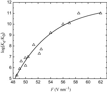
Figure summarizes the rates measured at 77 K. The relative field evaporation rate of the (110) Mo atomic planes is plotted as versus F. The best-fit curve in figure can be expressed by
where a1=11.7, a2=208, f1=28.43 V nm−1 and f2=5.83 V nm−1.
Figure 1 versus F plot for 〈 110〉-oriented molybdenum.
The maximum value of Chkl in our experiments was about 1000, which translates into an absolute field evaporation rate of surface atoms of about 1012 s−1. This is a reasonable value, close to the maximum of χe=1013 s−1 corresponding to the vibrational frequency of the surface atoms.
Computer simulation
The heavy computational load of advanced ab initio electronic structure calculations [Citation21] limits their application to relatively small atomic systems. To study complex processes such as plastic deformation and fracture, more computationally executable potentials must be used. We used the semi-empirical Finnis–Sinclair interatomic N-body potential constructed in [Citation22], which successfully describes the elastic, structural and cohesive properties of molybdenum. The methodology of the molecular dynamics calculation of ideal strength during the tensile test is described in detail in [Citation23]. We simulated molybdenum cylinders with diameters of 3.1, 6.2 and 15.7 nm and lengths of 6, 18 and 20 nm, respectively. Tension was realized by forcing the atoms into three (110) planes of the end surface. The absolute tension rate was constant and equal to 10 m s−1. This rate is much lower than that of the relaxation processes in the lattice, which are related to the atomic displacements. Hence, the computer-simulated tensile tests can be considered as quasi-static. We set stochastic vibration rates for the nanocrystal atoms that corresponded to the temperature of 77 K.
Results and discussion
The mechanical response was measured for 28 molybdenum needle-shaped specimens under a tensile load in the ‘nanostressing range’. Nanotip failure was apparent during the FIM experiment by a sudden increase in the field evaporation rate, which was accompanied by a current pulse and a bright flash of light between the electrodes. The mechanical behavior of the nanotips is correlated with the mechanical stress induced by the electric field in the FIM. The yield strength of perfect nanocrystals is usually much higher than the surface stress corresponding to the threshold of low-temperature field evaporation [Citation18]. Failure of the molybdenum nanotips was usually observed at high pulse voltages corresponding to a field evaporation rate in the range 106 to 109 layers s−1. At high rates of field evaporation, the ion space charge near the field emitter surface can be sufficient to reduce the applied field [Citation24] and the field induced mechanical loading determined by equations (Equation1) and (Equation2
). To investigate this possibility for molybdenum needle-shaped specimens, detailed estimations are required for the space charge effects at a high rate of field evaporation. Batrakov et al [Citation25] obtained a solution of Poisson's equation for needle-shaped electrodes subject to boundary conditions appropriate for the field electron current I, and in particular for a nonzero cathode field. It was shown that the actual field at the needle-shaped emitter can be expressed analytically in terms of the equation obtained for a spherical vacuum diode:
Here Fg is the geometrical electric field (found by solving the electrostatic equations), m and q are the mass and charge of the particles, respectively, R is the distance between the cathode and the anode and V=V0+Vp.
The geometrical electric field at the apex of a needle-shaped specimen is less than the value at the surface of a conducting sphere owing to the presence of the conical shank and can be given by [Citation19]
Here kf is the geometrical field factor, which depends on the taper angle of the emitter and has an approximate value of 5. The ion current density during field evaporation is
where S0 is the surface area per atom, n is the ion multiplicity and e is the elementary charge. Hence, for the case of field-ion emission, equation (Equation9
) leads to the expression
where Fa is the actual positive electric field at the apex of a specimen. Under a pulsed voltage, molybdenum atoms are field-evaporated as 2+ ions (n=2). For field evaporation of the molybdenum needle-shaped specimens, which are oriented along the 〈 110〉 direction, S0=7.1 Å2. Equation (Equation12
) may be used to analyze the space charge effects accompanying intensive field evaporation during the high-field mechanical testing of needle-shaped specimens.
The field strength F in figure is determined without theoretical consideration of the space charge effects and corresponds to Fg. If the ion emission is described by equations (Equation8), (Equation11
) and (Equation12
), the behavior of Fa(Fg) indicates that the specimens are partly screened by the ion space charge when Fg >55 V nm−1, as shown in figure . The inset shows a TEM image of the molybdenum tip formed by field evaporation at 77 K (r0=55 nm).
Figure 2 Real field at the specimen apex versus geometric field. 1, geometric field; 2, 3, and 4, obtained from equation (Equation12) with r0 equal to 14, 25 and 50 nm, respectively; the inset is a TEM image of a molybdenum tip formed by field evaporation at 77 K (r0=50 nm).
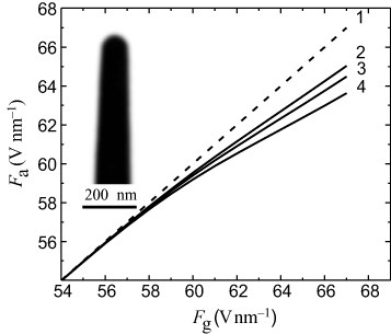
Analytical results Fa(Fg) are given for curvature radii at the apex of the specimen equal to 14, 25 and 50 nm. Comparing curves 1, 2 and 3, note that for a larger r0 the space charge screening of the electric field is stronger. The space charge effects when Fg ≤Fe0 are negligible for all values of the tip radius. Curves 2 and 3 correspond to the specimens subjected to field evaporation at the highest rates. The average field strength under the high-field mechanical loading of a specimen given by equation (Equation4) was determined by taking into account the difference between Fg and Fa shown in figure .
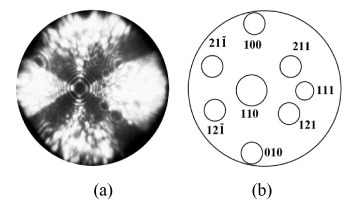
Figure shows the FIM image of a molybdenum specimen of 36 nm radius formed by field evaporation at V=8.28 kV. This characteristic image of a perfect single crystal consists of a large number of intersecting concentric rings related to the atomic terraces of prominent crystallographic planes on the specimen surface. There is no spiral structures characteristic of surface dislocations [Citation18]. Such images correspond to perfect crystals free of dislocations, planar defects and microcracks; they were typical for about 104 sections obtained by layer-by-layer field evaporation of the molybdenum specimens. The volume near the top of the needle-shaped specimens analyzed using an FIM is dislocation-free because the average dislocation spacing (300 nm) is much larger than the diameter of the specimens and the distance from the apex, at which a large tensile stress is attained (25–90 nm). Moreover, glissile dislocations are severely affected by field-induced stress. Most dislocations are removed from the tip of a nanorod by a mechanical stress, which are close to the ideal strength and owing to the image force from the metal surface [Citation26]. This phenomenon, termed ‘mechanical annealing’, was recently revealed to occur in several other nanocrystalline materials [Citation27, Citation28]. At the periphery of the FIM image in figure , one can see the specimen surface, which was not formed by field evaporation. It is characterized by nanoscale notches of depth 1.9–4.8 nm. The mechanism of this rupture was difficult to determine. In most cases nanotip failure was accompanied by electrical discharge of the capacitor determined by the microscope electrodes. Because of the small size of samples, they were heated to the melting point and became considerably blunted. Taking into account the fact that the pulse height Vp was characterized by comparatively low shot-to-shot reproducibility, in most tests the voltage pulses were kept as low as possible by maintaining an increased dc voltage, so that the error in determining the total voltage was about 2%. However, under this operating regime, the probability of specimens surviving the electrical discharge after the mechanical fracture of tips is extremely low, about 50% at 0 <V0/Vp<1.
Figure 3 FIM image of monocrystalline molybdenum nanorod before failure at 77 K (a) and corresponding stereographic projection (b).
Electrical breakdown in FIMs is initiated by the impact of nanoparticles detached from a specimen in a high electric field followed by the formation and expansion of the cathode plasma with velocity vc in the range (1–2)×104 m s−1 [Citation29]. The expanding plasma behaves as a dynamic capacitor plate characterized by a high velocity and a gigantic increase in the field strength at the specimen tip. The electrical discharge does not occur or is nondestructive if the voltage pulse is shorter than the time of plasma detachment: t<R/vc. Mechanical loading was performed in our experiments using a pulse generator with pulse duration t=20 ns, which is considerably shorter than R/vc. As a result, 6 of the 28 nanotips were ruptured without electrical discharge, and we managed to obtain FIM images of the failed surfaces. These images recorded at voltages of 0 <V0/Vp<1 usually exhibit narrow elongated patterns oriented along the [110] direction (figures (a) and (b)), and as V0/Vp→0 they take on the appearance of short streaks (figure (a)). During layer-by-layer field evaporation, broadening of the elongated images was observed. Similar failed surfaces were observed in FIM images of tungsten nanotips ruptured at stresses corresponding to a considerable fraction of the ideal strength [Citation30]; these images corresponded to the plastic mode of failure of monocrystals with the formation of a chisel-edge tip. In our samples, when V0/Vp>0.5, the peripheral parts of FIM images of failed specimens became wider owing to the evaporation of the chisel-like top under a constant voltage V0 (figure (b)).
Figure 4 FIM images of monocrystalline molybdenum nanocrystal after failure at 77 K at V0/Vp=0 (a) and V0/Vp=0.55 (b). The high-voltage pulse duration is 20 ns.
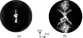
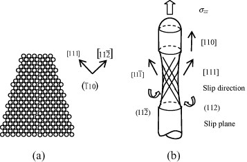
Figure (a) shows a tomographic 2D reconstruction of the wedge cross section adjacent to the plane obtained from a layer-by-layer field evaporation sequence. A crystallographic analysis showed that the chisel edge is oriented along the
direction, and the side surfaces of the wedge appear to be formed by atomic planes belonging to the
zone. The theoretical shear strengths are nearly identical for bcc metal slip systems { 211} 〈 111〉 and { 110} 〈 111〉 [Citation5]. For [110] oriented specimens, among the active slip planes only atomic {211} planes belong to the
crystallographic zone. A wedge neck can be produced in the gage part of the specimen by multiple gliding in the
and
slip systems, which are oriented at 35.3° to the [110] direction (figure (b)).
Figure 5 Tomographic 2D reconstruction of the chisel cross section obtained from a layer-by-layer field evaporation sequence (a) and sketch of chisel-edge-type failure due to plastic deformation of a nanotip (b).
The plastic behavior of 〈 110〉-oriented single-crystalline molybdenum nanocrystals, revealed in uniaxial tension tests, agrees well with the results of computer simulations [Citation23]. According to [Citation23], the transition from the elastic to plastic deformation of molybdenum nanocrystal under tension in the 〈 110〉 direction is associated with the local instability of the atomic lattice, which is accompanied by a tendency of a neck formation, primarily due to multiple slips in the 〈 111〉 { 112} deformation system. However, comparison of these computer simulations with experimental data reveals a substantial difference in the neck configurations. A specific feature of the lattice rearrangement in the molecular dynamic simulations is that it occurs within a highly localized region of the nanocrystal. As a result, the failure surface nearly coincides with the shear crystallographic and ( 112) planes. The angle between the failure surface and the loading axis was about 35°. The angle between the wedge surface and the specimen axis is in the range 12–16° and hence is not representative of the shear angle. Moreover, figures (a) and (b) reveal that the side surfaces of the wedge are neither planar nor atomically smooth. The nanosteps observed at the edge of the failure surface indicate that there may be some slippage on other systems. Figure shows the results for the tensile strength of the needle-shaped molybdenum obtained experimentally and by simulation. In the figure, σ is the breaking strength and D is the diameter of the nanocrystal in the region where the hemispherical cap joins the conical shank (z≈r0). The inset shows a TEM image of the tip after a chisel-like failure at Vp=6.50 kV and V0=5.47 kV.
Figure 6 Tensile strength of molybdenum nanocrystals at 77 K; the inset shows a TEM image of the molybdenum tip after chisel-edge-type failure.
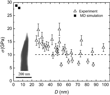
The largest values of tensile strength of 19.5 and 19.8 GPa were attained for the specimens with apex radius D/2 equal to 14 and 25 nm, respectively. For these specimens, the difference between the real field at the specimen apex and the geometrical field shown in figure corresponds to the space charge correction of σ, equal to 5.8 and 7.5%, respectively. The high-field loading corresponds to the soft testing method. In this case, the load cannot decrease during a specimen failure and remains above the value required for plastic deformation. Thus, mechanical testing in the FIM is an ideal soft testing method ensuring that a constant-force regime is maintained during the deformation. The error in high-field stress measurements due to inertial effects is negligible. It should also be noted that the hemispherical cap of the specimen is essentially under hydrostatic tension. This means that the shear stress in this area of the specimen vanishes, which renders it impossible to realize shears at the specimen apex formed by field evaporation. Two specimens were ruptured upon increasing the voltage before the onset field required for helium ionization was reached (about 30 V nm−1), and hence had a tensile strength of less than 4.0 GPa. The presence of a chemically active gas promotes the field evaporation process at a comparatively low field strength [Citation18]. This effect was used to reduce the probability of specimen failure during the preliminary formation of the hemispherical cap by field evaporation. Nitrogen was used as an active gas at a partial pressure of 2×10⁻⁵ Pa in 10−3 Pa helium. Nitrogen promoted the reduction of the evaporation field of molybdenum and ensured a decrease in field-induced stress during high-field forming from 9.78 to 1.77 GPa. After forming the hemispherical cap, the nitrogen was removed by a cryogenic getter. The field-induced tensile stress promoted the fracture of several specimens during the increase in dc field before the pulse testing. Six specimens were destroyed at an electric field less than that required for the onset of field evaporation in high vacuum (〈F0 〉=47 V nm−1); these specimens had a strength in the range 6.35–7.98 GPa. The dashed line in figure corresponds to the stress of 10 GPa induced by the field 〈F0 〉. The values of stress below this line correspond to those obtained by static mechanical testing, whereas the data above the line were obtained in the pulse regime. The maximum experimental breaking strength at 77 K is 19.8 GPa.
Because molecular dynamics simulations of nanocrystal failure are time-consuming, only three specimens with aspect ratios of 1.94, 2.90 and 1.27 were studied. The simulation data shown in figure correspond to a short-rod configuration, which is similar to the effective gage region of FIM nanotips. The calculated strengths are 28.8 and 27.9 GPa for diameters of 3.1 and 6.2 nm, respectively. The nanocrystal of 15.7 nm diameter is nearly isometric; its shape is considerably different from the experimentally studied nanotips, and therefore its strength (21.0 GPa) is not shown in figure . The maximum experimental values of the tensile strength of Mo agree with the results of calculations based on large diameters. Despite considerable scattering, a marked size effect is apparent, particularly at small diameters.
To present the strength in dimensionless form, the value of Young's modulus E for the [110] direction of tensile loading in the equilibrium ground state can be calculated from [Citation31]
where Cij are the elastic constants and α, β and γ are the direction cosines of the tensile axis. For the [110] direction, the angular term in equation (Equation13
) is equal to 0.5 and E110=264 GPa. In dimensionless form, the largest experimental value attained for the tensile strength (σmax=19.8 GPa=0.075 E110 for Mo) is nearly equal to that for W needle-shaped nanocrystals (σmax=28.3 GPa=0.069 E110) previously measured by us [Citation10]. These results are close to those obtained by theoretical calculations performed using ab initio methods [Citation4–8, Citation11]. The comparison of calculated results with FIM experiments [Citation10] suggested that the inherent strength of needle-shaped crystals is determined by the nucleation of dislocations at the free surface [Citation11]. Note that the theoretical tensile strength of molybdenum in the 〈 100〉 direction (σmax=0.078 E100 [Citation5]) is also essentially identical with our measured value of the dimensionless strength in the 〈 110〉 direction. A significant increase in compression strength when the diameter of molybdenum single crystals (nanopillars) was reduced to 200 nm was observed recently [Citation28]. The smallest 〈 001〉-oriented Mo nanopillar has a compressive strength of as high as 2.85 GPa. Considering that the ideal strength of 〈 110〉-oriented Mo is 1.37 times larger than that of 〈 110〉-oriented nanocrystals [Citation23], we may conclude that the results for our tensile testing of Mo nanoneedles agree well with those for the compressive testing of Mo nanopillars. All these agreements further validate our FIM measurements of the inherent tensile strength of perfect molybdenum nanocrystals.
From the molecular dynamic simulation of tension in bcc metal nanoparticles in the [110] direction it was shown [Citation23] that the formation of surface dislocations is the atomic mechanism responsible for the nanoparticle strength. It explains the wide range of experimental tensile strength values for defect-free molybdenum nanotips (from 6.3 to 19.8 GPa). Stress concentrators at the free surface, which facilitate the nucleation of dislocations, may be an additional reason for the above scattering. Nanoscale notches or grooves, which can be seen at the periphery of the FIM image in figure (a) and which formed during electrochemical etching, are examples of such concentrators. These surface irregularities and the atomic roughness may also be responsible for the broadening of the area of transition from the elastic to plastic deformation of molybdenum nanocrystals due to multiple slips in the 〈 111〉 { 112} deformation system; they resulted in a decrease in the angle between the failure surface and the loading axis as well as in the wedge angle.
The ideal strength is an intrinsic material characteristic determined by the crystal structure and atomic bonding. Likewise, the inherent strength of nanocrystals can be determined by the maximum stress under elastic instability (yield or fracture) when applying an increasing load to a finite, defect-free particle having a featureless surface. Although we know of no experimental data on the inherent tensile strength of molybdenum nanocrystals, the ideal shear strength has been measured in nanoindentation experiments and has been shown to be related to the nonlinearity in the stress–strain relation under tensile strain and to the triaxial state of stress [Citation13]. Considering these corrections, the maximum shear strength of molybdenum was reported to be 17.6–18.8 GPa. This value, within the accuracy of estimations, is equal to the ideal shear strength of molybdenum. Milstein and Chantasiriwan [Citation32] determined the theoretical ultimate tensile stress of molybdenum under [110] tensile loading. However, as shown in [Citation11] by comparing the experimental and theoretical data for [110] tensile loading, the nanocrystal might rupture at a load that gives a resolved shear stress close to the theoretical shear strength on a favorably oriented crystallographic plane. Failure in this case is expected to occur under a substantially smaller tensile loading. Our results demonstrate that the inherent (intrinsic) tensile strength of molybdenum nanocrystals is appreciably less than the ideal tensile strength of the material [Citation5, Citation7]. This reflects the early failure of nanotips determined by surface-induced dislocations rather than by the ideal strength of bulk Mo. This conclusion corresponds to the concept of the ideal strength as the maximum value of stress determined by the internal mechanical stability at temperatures close to 0 K. The strength of nanoparticles is controlled by the local instability of the crystal lattice that undergoes shearing [Citation23]. Stress relaxation occurs as a result of local plastic deformation and lattice reorientation (twin formation). The local nature of shear instability appears to be due to thermal oscillations resulting in a fluctuation of the local shear stress (phonon-induced instability) as well as to the presence of surfaces in nanoparticles [Citation23, Citation33].
Conclusions
Uniaxial tensile tests were performed using field-ion microscopy, which allowed us to test samples with nanoscale dimensions under ultrahigh loading stresses. The tensile strength and fractographic features of molybdenum nanotips were studied by an in situ high-field method involving mechanical loading with correction of the ion space charge. In this study we demonstrated the failure of nanocrystals inside an FIM, from which it was possible to deduce the failure stress, rupture topography and crystallographic failure parameters. FIM analysis showed that the nanocrystals before rupture were free of dislocations, presumably because of ‘mechanical annealing’ under mechanical stress close to the ideal electric field strength and owing to the image force from the metal surface. This finding is significant for precise determination of the inherent tensile strength of nanocrystals. It was shown experimentally that the plastic deformation of dislocation-free nanocrystals at low temperatures precedes their fracture, and it was confirmed that the strength of nanocrystals of bcc metals is controlled by local shear instability. FIM images after high-field mechanical testing indicate the plastic mode of failure of monocrystals with the formation of a chisel-edge tip by multiple gliding in the and
deformation systems.
According to the data obtained from uniaxial tension tests of 〈 110〉-oriented monocrystalline molybdenum needle-shaped specimens with the diameter at the apex varying between 25 and 90 nm, the Mo strength decreased from 19.8 to 6.3 GPa, respectively. This decrease in the tensile strength of dislocation-free molybdenum nanotips may be explained by both the decrease in strength of the needle-shaped specimens with increasing diameter (the size effect) and by the concentration of stress induced by atomic scale irregularities along the part of the needle-shaped specimen corresponding to the gage. The molecular dynamic simulation of tension in Mo nanorods predicted a decrease in strength from 28.8 to 21.0 GPa with increasing diameter from 3.1 to 15.7 nm. Although there is considerable scattering of the experimentally obtained values of strength, a marked size effect is also apparent. The maximum values of measured strength are thought to correspond to the inherent strength of Mo nanocrystals under uniaxial tension (19.8 GPa or 7.5% of Young's modulus).
Acknowledgments
We thank N Wanderka for helpful discussions and comments. This work was supported by the Program of the National Academy of Sciences of the Ukraine ‘Nanosystems, Nanomaterials and Nanotechnologies’ (Grant No. 30/07-H) and the NATO International Program No. SA (PST. CLG.976376) 5437.
References
- PolanyiM 1921 Z. Phys. 7 323 http://dx.doi.org/10.1007/BF01332803
- FrenkelJ 1926 Z. Phys. 37 572 http://dx.doi.org/10.1007/BF01397292
- KellyAMacmillanN H 1986 Strong Solids Oxford Clarendon
- ŠobMWangL GVitekV 1998 Phil. Mag. B 78 653
- LuoWRoundyDCohenM LMorrisJ W 2002 Phys. Rev. B 66 094110 http://dx.doi.org/10.1103/PhysRevB.66.094110
- ČernýMŠobMPokludaJŠanderaP 2004 J. Phys.: Condens. Matter 16 1045 http://dx.doi.org/10.1088/0953-8984/16/7/004
- ŠobMPokludaJČernýMŠanderaPVitekV 2005 Mater. Sci. Forum 482 33 http://dx.doi.org/10.4028/www.scientific.net/MSF.482.33
- LiuY-LZhangYZhouH-BLuG-HKohyamaM 2008 J. Phys.: Condens. Matter 20 335216 http://dx.doi.org/10.1088/0953-8984/20/33/335216
- OgataSLiJYipS 2005 Phys. Rev. B 71 224102 http://dx.doi.org/10.1103/PhysRevB.71.224102
- MikhailovskijI MPoltininP YaFedorovaL I 1983 Sov. Phys. Solid State 23 757
- RoundyDKrennC RCohenM LMorrisJ W 2001 Phil. Mag. A 81 1725 http://dx.doi.org/10.1080/01418610108216634
- GreerJ RNixW D 2005 Appl. Phys. A 80 1625 http://dx.doi.org/10.1007/s00339-005-3204-6
- WangY MMaE 2004 Appl. Phys. Lett. 85 2750 http://dx.doi.org/10.1063/1.1799238
- ChattopadhyaySChenL-CChenK-H 2006 Crit. Rev. Solid State Mater. Sci. 31 15 http://dx.doi.org/10.1080/10408430600689299
- MazilovaT IMikhailovskijI MKsenofontovV ASadanovE V 2009 Nano Lett. 9 774 http://dx.doi.org/10.1021/nl803399j
- KsenofontovV AMazilovaT IMikhailovskijI MSadanovE VVelicodnajaO AMazilovA A 2007 J. Phys.: Condens. Matter 19 466204 http://dx.doi.org/10.1088/0953-8984/19/46/466204
- NeklyudovI MSadanovE VTolstolutskajaG DKsenofontovV AMazilovaT IMikhailovskijI M 2008 Phys. Rev. B 78 115418 http://dx.doi.org/10.1103/PhysRevB.78.115418
- MillerM KCerezoAHeatheringtonM GSmithG D W 1996 Atom Probe Field Ion Microscopy Oxford Clarendon
- TsongT T 1990 Atom-Probe Field Ion Microscopy Cambridge Cambridge University Press
- SakuraiTMüllerE W 1973 Phys. Rev. Lett. 30 532 http://dx.doi.org/10.1103/PhysRevLett.30.532
- DerletP MNguyen-ManhDDudarevS L 2007 Phys. Rev. B 76 054107 http://dx.doi.org/10.1103/PhysRevB.76.054107
- FinnisM WSinclairJ E 1984 Phil. Mag. A 50 45 http://dx.doi.org/10.1080/01418618408244210
- KotrechkoS AFilatovA VOvsjannikovA V 2006 Theor. Appl. Fract. Mech. 45 92 http://dx.doi.org/10.1016/j.tafmec.2006.02.002
- IvanovB I 1974 JETP Lett. 20 72
- BatrakovA VPegelI VProskurovskijD I 1999 Tech. Phys. Lett. 25 454 http://dx.doi.org/10.1134/1.1262514
- GarberR IGeishericV SMikhailovskijI MFedorovaL I 1976 Fiz. Met. Metalloved. 42 155
- ShanZ WMishraR KAsifS A SWarrenO LMinorA M 2008 Nat. Mater. 7 115 http://dx.doi.org/10.1038/nmat2085
- BrinckmannSKimJ-YGreerJ R 2008 Phys. Rev. Lett. 100 155502 http://dx.doi.org/10.1103/PhysRevLett.100.155502
- MikhailovskijI MWanderkaNStorizhkoV EKsenofontovV AMazilovaT I 2009 Ultramicroscopy 109 480 http://dx.doi.org/10.1016/j.ultramic.2008.12.003
- GarberR IDranova ZhIMikhailovskijI MFridmanV Ya 1971 Sov. Phys. Solid State 13 339
- NyeJ F 1986 Physical Properties of Crystals: Their Representation by Tensors and Matrices New York Oxford University Press
- MilsteinFChantasiriwanS 1998 Phys. Rev. B 58 6006 http://dx.doi.org/10.1103/PhysRevB.58.6006
- KotrechkoSFilatovOOvsjannikovO 2007 Mater. Sci. Forum 567–568 65 http://dx.doi.org/10.4028/0-87849-469-3.65