Abstract
A new technique is proposed for the fabrication of fine patterns of molecular doping in organic–inorganic hybrid materials by the combination of capillary electrophoresis doping (CED) and photolithography. The UV-induced polymerization of bonds in organic groups yields a fine contrast of structures with the desired pattern in organic–inorganic hybrid films, and CED treatment introduces functional molecules only into unirradiated regions to form the doping patterns of molecules inside the films. The fine patterning of rhodamine-6G doping with from 2 to 4 μm resolution is demonstrated in hybrid films of 10 μm thickness.
Introduction
Organic–inorganic hybrid materials have been gathering much attention because of their high potentials for optical and/or biomedical devices at the atomic and/or molecular level [Citation1–4]. Investigations of stand-alone devices, such as light emitters, lenses, waveguides and detectors, have been carried out extensively and superior functionalities have been reported [Citation5–7]. At present, the integration of micrometer-sized components with various functions is essential for system devices [Citation8]. The high affinity of hybrid materials to both organic and inorganic materials is a great advantage for realizing multifunctionalities on the same platform. The doping of functional materials into the same platform is a key technology as observed in the fabrication of semiconductor devices. In organic–inorganic hybrid materials, the doping of functional ‘molecules’ is also attractive and the control of a fine doping structure on the micrometer scale is desirable.
Our group has developed a new technique of doping functional molecules and/or ions into films of organic–inorganic hybrid materials and demonstrated the doping of organic dyes for the fabrication of optical devices [Citation9]. The capillary electrophoresis doping (CED) technique involves the transport of molecules based on the electrophoresis phenomena in liquid under an applied electric field. The transported molecules are driven into the hybrid materials by the electric field. In a previous work [Citation10], we investigated the dependence of dye migration into organic–inorganic hybrid films on the prebake treatment of the films. The progress of the polymerization of hybrid materials during baking induced large changes in CED doping. In particular, when the hybrid films contained organic groups with curable units such as bonds, the thermal polymerization of
bonds proceeded to enhance the cross-linking of the structure of hybrid materials and effectively terminated the migration pathways of the doped molecules. From the relationship between the curing of organic groups and the migration behavior assisted by the electric field in hybrid materials, the photocuring procedure (photolithography) [Citation11–13] is expected to be compatible with the CED technique for developing a new process for the fabrication of ‘fine doping structures’. In this study, we demonstrated ‘molecular-doping lithography’ by utilizing CED and photolithography techniques, and obtained fine patterns with micrometer precision.
Experimental details
Preparation of organic–inorganic hybrid sols
Organic–inorganic hybrid materials were prepared by the sol–gel process. Triethoxyvinylsilane (TEVS, LS-2300, Shinetsu Chemical Co., Ltd), 3-methacryloxypropyltrimeth-oxysilane (MAPTMS, LS-3380, Shinetsu Chemical Co., Ltd), tetramethoxysilane (TMOS, T0588, TCI Co., Ltd) and titaniumtetra-isopropoxide (TTIP, Soekawa Chemical Co., Ltd) were used as the starting materials. Four types of sol were prepared, and their starting compositions are listed in table . As described in the following subsection, two types of hybrid film were prepared using these sols.
Table 1 Compositions of the raw materials of the prepared solutions (in mol%).
For Sol-1, TEVS was first hydrolyzed with aqueous HCl solution (pH 2) and ethanol by refluxing the TEVS:H2O:ethanol=1:3:3.5 mixture at 65 °C for 4 h. MAPTMS and TMOS were hydrolyzed separately in other solutions at room temperature for 2 and 1 h, respectively, with the molar ratios MAPTMS:H2O:ethanol=1:3:3.5 and TMOS:H2O=1:2 by HCl catalysis. Finally, three solutions were mixed and stirred at room temperature for 12 h.
For Sol-2 and Sol-4, MAPTMS was hydrolyzed with aqueous HCl solution (pH 2) at room temperature for 2 h, whereas MAPTMS:H2O=1:1.5. TMOS was hydrolyzed with another aqueous HCl solution (pH 2) with the molar ratio TMOS:H2O=1:2 at room temperature for 1 h. This TMOS solution was mixed with the first MAPTMS-sol and stirred for 24 h. TTIP i-PrOH solution was added to the former mixed solution and stirred at room temperature for 1 h. Finally, 3 mass% 1-hydroxycyclohexylphenylketone (IRGACURE 184, Ciba Special Chemicals Co., Ltd) was added as the photoinitiator of the polymerization of bonds.
For Sol-3, the same process as that for Sol-2 was employed except for the addition of IRGACURE184. This sol was diluted in ethanol with the volume ratio sol: ethanol=7:3 to have a viscosity adequate for fabricating films by the spin coating method.
Preparation of hybrid films
In this study, two types of film, namely a buried optical waveguide and a photopatterned film were prepared using the four organic–inorganic hybrid sols described above. Figure shows a schematic cross section of the buried optical waveguide. Clad-1, Clad-2 and Core were prepared from Sol-1, Sol-2 and Sol-3, respectively. First, Sol-1 was coated onto indium tin oxide (ITO)-coated slide glass by dip coating. The drawing speed and atmosphere were 300 mm min−1 and dry nitrogen, respectively. The obtained layer was heated to 60 °C for 12 h in nitrogen atmosphere, and then, it showed a thickness of 2 μm. Subsequently, Sol-2 was deposited on Clad-1 by dip coating under the same drawing conditions. After heating to 60 °C for 15 min in nitrogen atmosphere, the sample was irradiated for 2 min with UV light from an ultrahigh-pressure mercury lamp (USHIO, USH-250D; 30 mW cm−2 at 365 nm) through a photomask to obtain a grooved structure of 20 μm width. After rinsing the unirradiated part (line) with i-PrOH, the films were baked at 60 °C for 4 days under nitrogen atmosphere (Clad-2). Finally, Sol-3 was deposited on Clad-2 by spin coating (2000 rpm) and baked at 60 °C for 7 h under nitrogen atmosphere (Core).
Figure 1 Illustration of the cross section of the designed buried-type optical waveguide.

The photopatterned film was fabricated from Sol-4 on ITO-coated slide glass by dip coating. The drawing speed and atmosphere were 300 mm min−1 and dry nitrogen, respectively. This film was baked at 60 °C for 4 h under nitrogen atmosphere; the film thickness was 10 μm. This film was also irradiated for 2 min with the same mercury lamp through a photomask to produce photopatterns with various sizes inside it. Then, this film was CED-treated without rinsing.
Capillary electrophoresis doping of rhodamine-6G
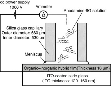
Figure shows a schematic illustration of the CED technique. In this study, a silica glass capillary with an outer diameter of 660 μm and an inner diameter of 530 μm was used. Details of the CED technique have been reported elsewhere [Citation9, Citation10]. Rhodamine-6G (R6G), a laser dye with the highest quantum efficiency, was dissolved in a mixture of n-hexanol and EtOH (90:10 vol%). The R6G concentration was 1×10⁻³ M. In the CED treatments, 1000 V DC was applied for 2 min between one end of the capillary and the ITO electrode on the slide glass. The current through the CED circuit was recorded. The doped areas were observed under an optical microscope and a confocal laser scanning microscope (Nanofinder®, Tokyo Instruments, Inc.).
Figure 2 Schematic illustration of the capillary electrophoresis doping technique.
Results
CED treatment of buried-type optical waveguide
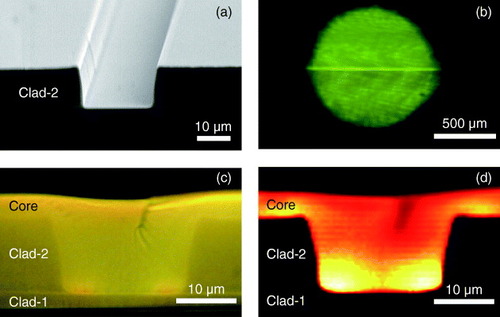
Figure (a) shows a scanning electron microscopy (SEM) image of the fabricated grooved structure of Clad-2. The cross section of the concave structure for the core part is slightly trapezoidal with a smaller width at the bottom than at the top. Figure (b) shows the top view of the CED-treated part of the buried waveguide. A green circular part with a bright line is observed and corresponds to the CED-treated area. Figures (c) and (d) show its cross sections viewed under the optical and confocal laser scanning microscopes, respectively. Figure (c) shows the clear interfaces between Clad-1/Core and Clad-2/Core and the buried waveguide with the designed dimensions. Confocal image (d) presents the intensity map of fluorescence (λ=540–580 nm) from the R6G dye molecules inside the film. Fluorescence is detected from the Core part only, and its shape is the same as that of the Clad/Core interface in figure (c), showing that R6G molecules were successfully doped into the Core part only.
Figure 3 Structure of the fabricated waveguide. (a) SEM image of the grooved Clad-2 layer and (b) top view of the CED-treated part. Cross sections of the waveguide viewed under the (c) optical and (d) confocal laser scanning microscopes.
CED treatment for fine pattering
Figure shows a composition of the fluorescence intensity images of the UV-irradiated part (through the photomask after the CED treatment) with the test patterns in the photomask. These images were obtained with the confocal laser scanning microscope. From (a) to (c), the aperture width of the slit in the photomask decreases from 12 to 2.2 μm. The fluorescence images reproduce well the patterns in the photomask. To examine the spatial resolution of the doping pattern formation, the distances between the points giving 90 and 10% of the maximum fluorescence intensity were evaluated as 4.2, 4.4 and 1.1 μm for 12, 4.0 and 2.2 μm stripes, respectively. From these values, a spatial resolution of less than 4 μm was attained for the film with a thickness of 10 μm.
Figure 4 Comparison of the fluorescence intensity images of the doped rhodamine-6G molecules with images of the photomask: (a) stripes with an aperture width of 12 μm, (b) number ‘3’ with an aperture width of 4.0 μm and (c) stripes with an aperture width of 2.2 μm. Images were recorded using the confocal laser scanning microscope.
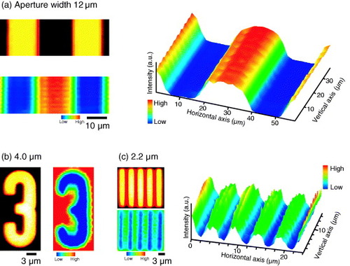
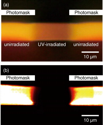
Figure shows the cross-section of the films prepared using Sol-4 and subjected to photopatterning by UV irradiation and CED treatment. The width of the slit in the photomask was 20 μm. The images confirm that R6G molecules were not doped into the UV-irradiated part. The boundaries between the doped and undoped regions showed bending and a slight diffusion with a length of several micrometers. These are due to the low resolution of the photolithography process. The spatial resolution observed in the doped pattern in figure is attributed to this boundary diffusion.
Figure 5 Cross section of R6G-doped films, UV irradiated through the photomask: (a) optical microscopy image and (b) fluorescence image obtained with a confocal laser scanning microscope. White bars schematically represent the photomask pattern.
Discussion
CED treatment enables the migration of charged molecules into the hybrid films by the driving force of the applied electric field. In our previous paper [Citation10], it was clarified that an appropriate amount of spaces in the hybrid materials is necessary for controlling the migration and occupation by doped molecules. Prebake treatment, which is generally employed to promote the densification and polymerization of the constituent alkoxides, changes the structure of hybrid materials altering the migration behavior of doped materials. From the isothermal gravimetry and differential thermal analysis (TG-DTA) and Fourier-transform infrared absorption spectra, the polymerization of the bonds in methacryloxy and vinyl groups in MAPTMS and VETS, respectively, was found to be important for terminating the migration of the R6G molecules, in addition to the dehydration reactions of the –OH groups. Both the thermal curing and photocuring of the
bonds reduce the migration of molecules. The polymerization of the
bonds enhances the cross-linking between the inorganic chains of Si–O–Si and Si–O–Ti through the organic groups. In this study, the photoinduced polymerization of the
bonds was carried out to define the small regions where the molecules migrated. The employed heating conditions are chosen to allow the migration of R6G molecules only when the electric field assists the doping. The addition of the photoinitiator IRGACURE184 effectively initiates the radical polymerization between the
bonds via UV irradiation and induces a chain reaction [Citation14–17]. Using this characteristic reaction, the photolithography patterning of hybrid materials for the optical devices has been investigated. In the case of the CED treatment, it terminates the migration pathways of doped molecules and finally embosses the doping pattern of the functional molecules in hybrid films.
As shown in figures and , photocuring terminates the migration of R6G. Patterned doping would be successful if a large contrast of the molecular migration could be induced between the UV-irradiated and unirradiated parts. To evaluate the effect of the radical polymerization of bonds on the molecular migration, the electric currents during the CED treatment were compared between the as-heat-treated unirradiated film (#1) and the film (#2) photocured by UV irradiation for 2 min; both films were prepared from Sol-4 (figure ). UV irradiation reduces the CED current by almost two orders of magnitude. The obtained extremely small current indicates the presence of few mobile charged chemical species in the irradiated film. As observed by Sasaki et al [Citation18], one might consider that the photocatalytic effect of the TiO2 component would change the structure of the hybrid film. However, it is a very slow process to observe its effect on the film structure. The photoinduced reactions in our study should be simply attributed to the chain reactions due to the photoinitiator that induces the polymerization of
bonds as the dominant factor rather than the photocatalytic effect of TiO2. Figure includes the currents of the CED treatments of the UV-irradiated (#3) and unirradiated (#4) films without the photoinitiator; both films were prepared from Sol-3. Their currents were similar to that of the UV-unirradiated film with the photoinitiator. In addition, the CED doping of R6G under the same conditions was also available into these films (#1, 3, and 4). This indicates that the combination of UV light and the photoinitiator is important. Photopolymerization due to the chain reaction by the photoinitiator surely enables the formation of the structural contrast of soluble/insoluble and dopable/undopable regions in the film, as respectively shown in figures (a) and .
Figure 6 Currents during the CED treatments of the films prepared under various conditions: #1 (blue line) UV-unirradiated film with photoinitiator (IRGACURE184), #2 (red line) UV-irradiated film with photoinitiator (IRGACURE184), #3 (orange line) UV-irradiated film without photoinitiator and #4 (green line) UV-unirradiated film without photoinitiator.
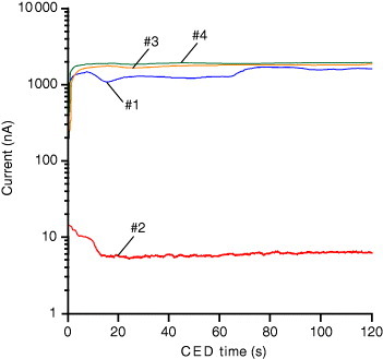
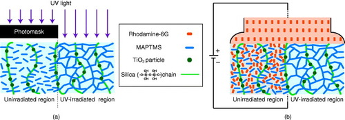
Figure schematically shows the UV-irradiation effect on the formation of the doping pattern. Radical polymerization by the photoinitiator induces further hybrid network cross-linking and film densification. It also eliminates the mobile charged species and suppresses the migration of molecules into the hybrid film. The extremely high contrast of the hybrid structure after UV irradiation enables the formation of fine patterns due to the difference in molecular migration. The optimization of the conditions of hybrid film preparation and photolithography would result in even finer patterns inside the hybrid film than those achieved in this work. It would also provide valuable techniques of fabricating sophisticated patterns of doping in organic–inorganic hybrid materials for functional devices, such as ‘molecular-doping lithography’.
Figure 7 Schematic illustrations of the effect of UV irradiation on the hybrid film and the migration of rhodamine-6G molecules: (a) photopolymerization between MAPTMS units in the irradiated region and (b) migration of rhodamine-6G molecules into the unirradiated region. In the UV-irradiated part, the cross-linking of MAPTMSs prevents the migration of R6G molecules.
Conclusion
The photolithography technique has been combined with the capillary electrophoresis doping (CED) technique to form fine molecular doping patterns in organic–inorganic hybrid films. The radical polymerization initiated by IRGACURE184 induced a high contrast of the migration behavior of rhodamine-6G molecules into the films by the CED treatment, and fine patterned doping with a spatial resolution of from 2 to 4 μm was attained.
References
- YueJYanLSiJChenFYangQHouXQianGGuoJ 2009 Opt. Commun. 282 1448 http://dx.doi.org/10.1016/j.optcom.2008.12.043
- JonesJ R 2009 J. Eur. Ceram. Soc. 29 1275 http://dx.doi.org/10.1016/j.jeurceramsoc.2008.08.003
- KangXWangJTangZWuHLinY 2009 Talanta 78 120 http://dx.doi.org/10.1016/j.talanta.2008.10.063
- DamiaCSharrockP 2006 Mater. Lett. 60 3192 http://dx.doi.org/10.1016/j.matlet.2006.02.071
- FengJZhangH JPengC YYuJ BDengR PSunL NGuoX M 2008 Micropor. Mesopor. Mater. 113 402 http://dx.doi.org/10.1016/j.micromeso.2007.11.041
- JiangHYuanXYunZChanY CLamY L 2001 Mater. Sci. Eng. C 16 99 http://dx.doi.org/10.1016/S0928-4931(01)00282-X
- JabbourJEtienneS CSmaïhiMGattiSKribichRPilleGMoreauTEtienneP 2007 Appl. Surf. Sci. 253 8032 http://dx.doi.org/10.1016/j.apsusc.2007.02.079
- YangSAizenbergJ 2005 Mater. Today 8 40 http://dx.doi.org/10.1016/S1369-7021(05)71288-8
- YanoTTaguchiJSegawaHShibataS 2006 Proc. SPIE 6123 61230W http://dx.doi.org/10.1117/12.647382
- TaguchiJYanoTSegawaHShibataS 2009 J. Ceram. Soc. Japan submitted
- YanHZhaoYQiuCWuH 2008 Sensors Actuators B 132 20 http://dx.doi.org/10.1016/j.snb.2008.01.002
- LeeF YFungK HTangT LTamW YChanC T 2009 Curr. Appl. Phys. 9 820 http://dx.doi.org/10.1016/j.cap.2008.07.017
- CopperwhiteROubahaMVersaceD LBarghornC CMacCraithB D 2008 J. Non-Cryst. Solids 354 3617 http://dx.doi.org/10.1016/j.jnoncrysol.2008.03.026
- BednarBKralicekJZachovalJ 1993 Materials Science Monographs Amsterdam Elsevier p 76
- GruberH F 1992 Prog. Polym. Sci. 17 953 http://dx.doi.org/10.1016/0079-6700(92)90006-K
- VersaceD LOubahaMCopperwhiteRCroutxe-BarghornCMacCraithB D 2008 Thin Solid Films 516 6448 http://dx.doi.org/10.1016/j.tsf.2008.02.028
- JeongSMoonJ 2005 J. Non-Cryst. Solids 351 3530 http://dx.doi.org/10.1016/j.jnoncrysol.2005.08.029
- SasakiTMatsudaATadanagaKTatsumisagoM 2005 J. Ceram. Soc. Japan 113 519 http://dx.doi.org/10.2109/jcersj.113.519