Abstract
Thermal conductivity is one of the key parameters in the figure of merit of thermoelectric materials. Over the past decade, most progress in thermoelectric materials has been made by reducing their thermal conductivity while preserving their electrical properties. The phonon scattering mechanisms involved in these strategies are reviewed here and divided into three groups, including (i) disorder or distortion of unit cells, (ii) resonant scattering by localized rattling atoms and (iii) interface scattering. In addition, we propose construction of a ‘natural superlattice’ in thermoelectric materials by intercalating an MX layer into the van der Waals gap of a layered TX2 structure which has a general formula of (MX)1+x(TX2)n (M=Pb, Bi, Sn, Sb or a rare earth element; T=Ti, V, Cr, Nb or Ta; X=S or Se and n=1, 2, 3). We demonstrate that one of the intercalation compounds (SnS)1.2(TiS2)2 has better thermoelectric properties compared with pure TiS2 in the direction parallel to the layers, as the electron mobility is maintained while the phonon transport is significantly suppressed owing to the reduction in the transverse phonon velocities.
Introduction
The strong dependence of human society on fossil fuels has lead to political unrest and global climate change [Citation1]. Thermoelectrics as materials of sustainable energy technology can offer a promising solution for this energy and environmental crisis. By taking advantage of the Seebeck effect, thermoelectric materials can generate electricity from the waste heat of automobile exhaust and various industrial processes. However, thermoelectrics are currently too inefficient for most practical applications. The efficiency of thermoelectric materials can be evaluated by the figure of merit ZT=S2σT/k, where S, σ and k represent the Seebeck coefficient, electrical conductivity and thermal conductivity, respectively. The thermal conductivity has two components, the lattice component kl and the electronic component ke, and ke is proportional to σ according to the Wiedemann–Franz law. To maximize the ZT value, the concept of ‘phonon glass electron crystal’ was proposed, which states that the phonons transport should be suppressed, as in glasses, and the electrical conductivity should be maintained as in crystals. Over the past decade, most progress in thermoelectric materials has been made by reducing lattice thermal conductivity, and a brief review of the reduction strategies is given below.
Thermal transport in solids is the dissipation of vibrational energy between adjacent atoms through chemical bonds. In the quantum theory, it is considered as the energy transfer between phonons. By applying the phonon gas theory, the thermal conductivity of a three-dimensional isotropic system can be written as:
1 where Cv, l and v stand for the heat capacity, phonon mean free path and phonon velocity, respectively. The situation is complicated by the broad spectrum of phonon frequencies in a solid. High-energy optical phonons do not have sufficiently high group velocities to transport an appreciable quantity of heat, and thus the thermal transport is frequently dictated by the longer-wavelength acoustic phonons [Citation2]. Therefore, the phonon velocity can be approximated by the mean sound velocity. The heat capacity can well be described by the Debye model or, in some cases, by the Einstein model. At temperatures higher than the Debye temperature, Cv equals 3kB for each atom, where kB is the Boltzmann constant. The sound velocity is determined by the atomic bonding and density. In most cases, for a given material, both Cv and v are related to the intrinsic properties and are almost insensitive to the structural changes that results in low tunability. The phonon mean free path, l, is the maximum distance the phonons can travel; it can be affected by various scattering events. The strategies to suppress l and kl that have been developed in the thermoelectric field can generally be divided into three groups: disorder or distortion of unit cells, resonant scattering by localized rattling atoms and creation of a high density of interfaces. It should be mentioned that the phonon mean-free path cannot be shorter than the average inter-atomic spacing in a homogeneous system (but it can be shorter in an inhomogeneous system, such as a soft superlattice).
Strategies for reducing the thermal conductivity
Disordering or distorting unit cells
Unit cells can be disordered by introducing point defects, such as substitution atoms, vacancies or interstitials. Wood [Citation3] first proposed the idea that the figure of merit of a compound could be increased by forming a solid solution with a compound of similar electronic valence structure but different atomic masses. The reasoning was that the local distortion produced by introducing a foreign atom of similar valence does not appreciably scatter-free charge carriers (with their long wavelengths) but strongly scatters phonons. Thus, the thermal conductivity can be lowered without seriously affecting the electrical conductivity. This method was proved efficient for nearly all thermoelectric material systems. One interesting result is observed for Mg2Si1−xSnx. Not only the thermal conductivity is suppressed but also the electrical properties are improved, because the substitution of Si with Sn increases the density of states in the conduction band, while the electron mobility is maintained [Citation4].
The phonon scattering by point defects is determined by the mass, size and interatomic force differences between the substituted and original atoms. In 1963, Abeles incorporated the size and interatomic force differences into the strain field fluctuation and formulated them in terms of the size difference only [Citation5]. The conclusion of that model is that to maximize the phonon scattering, one should choose the atom that has the largest mass and size differences with the atom to be substituted.
According to the above discussion, vacancy should be a more efficient point defect, as it can scatter phonons by virtue of both missing atom and missing interatomic linkages. A dramatic reduction in thermal conductivity was found in vacancy-rich SrxLa1−xTiO3−δ [Citation6] La1−xTe4 [Citation7] and Mg2Si1−ySby [Citation8]. However, vacancies may act as electron acceptors, thereby modifying the electronic transport properties and even worsening the thermoelectric performance.
In the Rayleigh scattering regime, the scattering cross section of a point defect varies as σ∼b6/λ4, where λ is the phonon wavelength and b is the size of the scattering particle; for atomic substitutions in alloys, b ∼ 1 Å. This relation suggests that point defects are effective in scattering short-wavelength phonons or Brillouin zone edge phonons but have less effect on longer wavelength phonons. Therefore, a limit of thermal conductivity reduction arises, which is called the alloying limit. A larger thermal conductivity reduction can be achieved by adding other mechanisms, such as grain boundaries, that can scatter phonons of longer wavelengths.
Not only atomic disorder but also the disorder of valence at a certain atomic site (valence fluctuation) can strongly reduce the thermal conductivity. In Tl9BiTe6, the Bi3+ and Tl+ ions are distributed randomly at the 4c site, introducing the valence disorder [Citation9]. A pronounced reduction in the lattice thermal conductivity was observed and attributed to the strong phonon scattering by the different valence states at this 4c site. In NaxCoO2, the randomly distributed Na+ ions induce Co3+/Co4+ valence fluctuations, and a calculation suggests that they can also contribute to the low thermal conductivity of NaxCoO2 (1.77 W m−1 K−1 at room temperature) [Citation10].
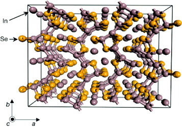
Peierls distortion is a new mechanism of reducing thermal conductivity in order to boost the thermoelectric performance [Citation11]. In the quasi-one-dimensional In4Se3 crystal (figure ), Peierls instability of the chain-like structure along the b-axis gives rise to the charge density wave which breaks the translation lattice symmetry (lattice distortion) by the strong electron–phonon interaction. Therefore, the thermal conductivity of In4Se3 could be significantly reduced and the ZT value reached 1.48 at 705 K.
Figure 1 Crystal structure of In4Se3. Perspective view of the a–b plane. Covalently bonded In–Se layers are stacked along the a-axis by the relatively strong van der Waals interactions (reproduced with permission from [Citation11] © 2009 Nature Publishing Group).
Resonant scattering by localized rattling atoms
Filled skutterudite antimonides are cubic compounds with the formula RM4Sb12, where R is a rare-earth element (such as La or Ce) and M is a transition metal (for example, Fe or Co) [Citation12]. The rare-earth ion is weakly bound in an oversized atomic cage formed by the other atoms, giving rise to localized, incoherent vibrations. Its presence dramatically reduces the lattice component of the thermal conductivity while having little effect on the electronic properties of the compound. This combination of properties makes filled skutterudites potentially interesting thermoelectric materials.
Localized rattling atoms are also found in clathrates, such as Sr8Ga16Ge39 and Ba8Ga16Ge30 [Citation13]. These compounds have cubic structures, the same as in the type-I ice clathrates. These structures can be thought of as tetrahedral frameworks of Ga and Ge atoms; they form large cages of 20 or 24 atoms that surround the Sr or Ba atoms. The alkaline-earth atoms in the larger cage have an unusual atomic displacement parameter showing a sign of localized vibrations. The glass-like heat conductivity arises from resonant scattering of phonons by vibrations of the dopant ions in their polyhedral cages. The relatively high charge-carrier mobility of these clathrates indicates that the dopant–cage interactions do not substantially degrade the electronic properties.
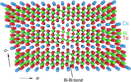
In CsBi4Te6, the Cs+ ions are intercalated between the [Bi4Te6] layers as shown in figure [Citation14]. Such confinement restricts the motions of the Cs+ ions in the direction perpendicular to the crystal b-axis. Therefore, the Cs+ ions act as ‘rattlers’ and the localized vibrations are strongly coupled with the framework via anticrossing of ‘localized’ rattling vibrations into acoustic branches of the same symmetry. This results in resonant scattering of phonons and reduction in the thermal conductivity.
Figure 2 Crystal structure of CsBi4Te6 (reproduced with permission from [Citation14] © 2000 American Association for the Advancement of Science).
It should be mentioned that a recent lattice dynamic calculation of neutron scattering in skutterudites indicates that the vibrational modes of the ‘rattler’ are coherently coupled with the host-lattice dynamics [Citation15]. The mechanism of resonant scattering is questioned, but it is conceivable that the disorder of partial filling of the ‘rattler’ may generate isolated energy dissipation centers [Citation15].
Interface scattering
Phonons can be scattered by interfaces of different phases (hetero-interface) or interfaces between randomly oriented grains (grain boundary). There mechanisms were recently realized in the novel techniques to synthesize nanostructured materials where the number of interfaces is maximized to increase the phonon scattering.
The lowering of thermal conductivity by reducing the grain size was first realized in 1981 in polycrystalline silicon germanium alloys. Compared with single crystals of SiGe alloys, polycrystalline SiGe with grains of the order of 1 μm showed higher ZT values [Citation16].
Many techniques were developed to produce bulk material consisting of nanograins. These techniques generally involve two steps. One is the fabrication of small crystalline or even amorphous particles by chemical reaction or special processing of coarse raw materials that may include metallic alloying, high-speed ball milling [Citation17] and melt spinning [Citation18]. The second step is fast sintering of the powders using spark plasma sintering or short-time hot pressing that can densify the powders without significant grain growth.
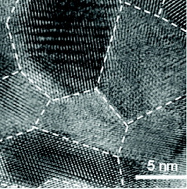
The problem of the nanograin route is that the electrical conductivity is reduced by the grain boundaries. One solution is to have coherent interfaces, so that the grain-boundary scattering of electrons can be prevented and the electronic conductivity can be maintained. Xie et al [Citation18] used melt spinning followed by quick spark plasma sintering to fabricate high-performance p-type Bi0.52Sb1.48Te3 bulk material with unique microstructure. As shown in figure , this microstructure consists of nanocrystalline domains embedded in amorphous matrix, and the domains include 5–15 nm nanocrystals with coherent grain boundaries. The thermal conductivity was reduced by the grain boundaries, but the electrical conductivity was maintained that yielded ZT of 1.56 at 300 K.
Figure 3 Nanograins of Bi0.52Sb1.48Te3 bulk material with coherent grain boundaries (reproduced with permission from [Citation18] © 2009 American Institute of Physics).
Another solution is to fabricate nanostructured bulk thermoelectric materials by spontaneous partitioning of a precursor phase into thermodynamically stable phases. For example, crystals pulled from an InSb–Sb eutectic alloy, which forms rods of Sb as thin as 4 μm in the InSb matrix, show a clear decrease in thermal conductivity with decreasing rod diameter, both parallel and perpendicular to the rod axis [Citation19]. However, because the interfaces were coherent, no significant reduction in electrical conductivity or Seebeck coefficient was observed.
Beside nanograin solids, other low-dimensional materials were also fabricated, including nanotubes and nanowires. Bi2Te3 nanotubes were synthesized and sintered into bulk compacts [Citation20]. Their thermal conductivity was significantly reduced compared to Bi2Te3 crystals, but the electrical conductivity was also decreased that resulted in only a minor improvement in the ZT value. Silicon nanowires with diameter of about 50 nm were also investigated and their thermal conductivity exhibits 100-fold reduction compared with bulk silicon, yielding ZT=0.6 at room temperature [Citation21].
Nanoinclusions were proven to be effective in reducing the thermal conductivity, as demonstrated by embedding ErAs nanoparticles into the In0.47Ga0.53As matrix [Citation22]. The inclusions were about 5 nm in size and were separated by an average distance of 5–40 nm that resulted in strong scattering of the mid-to-long wavelength phonons. Meanwhile, the point defects in In0.47Ga0.53As scattered the short-wavelength phonons. The combined effect was to significantly lower the lattice thermal conductivity and improve the ZT value. Since then, various nanodots or nanoinclusions were incorporated into bulk materials and became an important part of the recent development of thermoelectric materials [Citation23, Citation24].
The lowest thermal conductivity (0.05 W m−1 K−1 for WSe2 films) was obtained however with a superlattice structure [Citation25]. A successful example of applying such structure in thermoelectric materials is periodically stacked Bi2Te3 and Sb2Te3 compounds [Citation26]. In the direction perpendicular to the interface of the two materials, the lattice thermal conductivity was reduced to 0.22 W m−1 K−1, which is almost a half of the minimum value for the individual components, because of the acoustic mismatch between the superlattice components. However, owing to the small valence and conduction band offsets between Bi2Te3 and Sb2Te3, the electron mobility was not altered much. Therefore, the resultant ZT value approached 2.4 in the cross-plane direction at room temperature.
A modulated elemental reactants method was later developed to make misfit-layer dichalcogenide films of (PbSe)m(QSe2)n (Q=W or Mo, m=1–5, and n=1–5), and the thermal conductivities of these layered materials with nanoscale thickness fall below the predicted minimum thermal conductivity of their individual components [Citation27].
Most phonons can pass through the interface between dissimilar materials if those materials have similar crystalline and elastic properties, but the phonons will be reflected back if this difference is large. Balandin and Wang [Citation28] considered a quantum well structure by sandwiching bismuth-telluride thin films between layers of a polymer or another ‘soft’ dielectric substance. The phonons of the Bi2Te3 layer cannot pass through the interface between Bi2Te3 and the polymer layer because of distinctively different elastic properties. Therefore, the phonons are spatially confined within the Bi2Te3 layer. Calculations show that strong modification of the phonon group velocities and dispersion due to spatial confinement leads to a significant increase in the phonon relaxation rate and hence in a strong reduction in the lattice thermal conductivity.
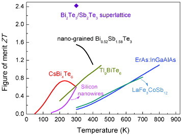
In summary, various phonon scattering mechanisms were employed in the recent development of thermoelectric materials. The ZT values of these materials are summarized in figures and .
Figure 4 ZT values of n-type thermoelectric materials, including Bi2Te3 [Citation20], Bi2Te3 nanotube composite [Citation20], Ag0.8Pb22.5SbTe20 [Citation24], In4Se3-δ [Citation11], Mg2Si0.4Sn0.6 [Citation4] and (SnS)1.2(TiS2)2 [Citation29].
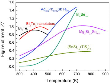
Figure 5 ZT values of p-type thermoelectric materials, including Bi2Te3/Sb2Te3 superlattice [Citation26], nanograined Bi0.52Sb1.58Te3 [Citation18], CsBi4Te6 [Citation14], Tl9BiTe6 [Citation9], silicon nanowires [Citation21], LaFe3CoSb12 [Citation12] and ErAs embedded in the InGaAlAs matrix [Citation34].
The concept of ‘natural superlattice’
Nanostructures and artificial superlattices have significantly lowered the thermal conductivity and thereby improved the thermoelectric performance. However, it is still challenging to maintain their structural stability at high temperatures given the complexity of the multi-component phase equilibrium. Therefore, we proposed the idea of a ‘natural superlattice’ produced by intercalating a layer of SnS into the van der Waals gap of layered TiS2 [Citation29, Citation30]. The TiS2 layer can provide thermopower as well as the electron pathway according to Imai's research on TiS2 single crystals [Citation31]. The intercalated SnS layer can suppress the transport of phonons as a consequence of the interaction between the SnS layer and TiS2 layer and/or disruption of the periodicity of TiS2 in the direction perpendicular to the layers. The conventional pressure sintering techniques (hot pressing or spark plasma sintering) produced highly oriented layers of polycrystalline grains owing to anisotropic bonding in this natural superlattice. This natural superlattice also shows high stability of thermodynamic and thermoelectric properties.
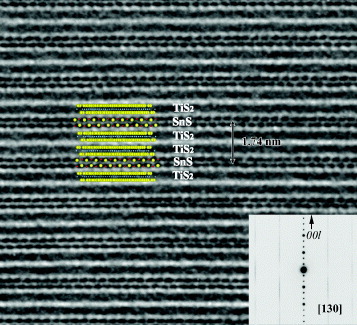
The SnS layer and the paired TiS2 layers stack in the direction of c axis, although the c axes of the two subsystems slightly diverge. Inside the layers, the b axes are parallel and have equal lattice constants. The a axes are also parallel, but the corresponding lattice constants have a ratio of about 3:5. Therefore, the value of 1.2 in the chemical formula of (SnS)1.2(TiS2)2 is obtained by considering the ratio of lattice parameters and the number of atoms in the unit cells. The atomic structure of (SnS)1.2(TiS2)2 along the [130] zone axis is shown in figure [Citation29]. The paired TiS2 layers and single SnS layer stack alternatively, composing the unit cell with the length of 1.74 nm. The SnS layers are stacked with completely random transverse displacement normal to the c-axis that can further be evidenced by the presence of diffuse streaks in the electron diffraction pattern. The lack of correlation between the successive SnS layers gives rise to planes of diffuse intensity instead of well-defined reflections.
Figure 6 HRTEM image of (SnS)1.2(TiS2)2 along the [130] zone axis.
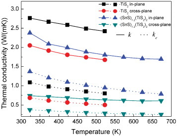
The thermal conductivities of TiS2 and (SnS)1.2(TiS2)2 are plotted in figure as a function of temperature. (SnS)1.2(TiS2)2 has a lower thermal conductivity than TiS2 in the whole temperature range, for both the in-plane and cross-plane directions. The electronic thermal conductivity (ke) is directly related to the electrical conductivity through the Wiedemann–Franz law, ke=L0Tσ, where the Lorenz number L0 is 2.44×10⁻⁸ W Ω K−1. The ke values for these (MS)1+x(TiS2)2 compositions were calculated and added to figure . They are rather similar for TiS2 and (SnS)1.2(TiS2)2 in both the in-plane and cross-plane directions demonstrating that the main reason for the reduction of the thermal conductivity is the decrease in the lattice thermal conductivity.
Figure 7 Thermal conductivity (k) and its electronic component (ke) for TiS2 and (SnS)1.2(TiS2)2 in the in-plane and cross-plane directions.
The lattice thermal conductivity values are presented in figure [Citation29]. They are much lower for (SnS)1.2(TiS2)2 than TiS2 along both the in-plane and cross-plane directions. The minimum thermal conductivity can be calculated for this composition as [Citation32]
2 Here the sum is taken over the two transverse and one longitudinal sound modes, and the values of speed of sound vi are summarized in table ; θi is the Debye temperature for each polarization which can be expressed as [Citation32]
3 Here n is the number density of atoms and the results are listed in table .
Figure 8 Lattice thermal conductivity of TiS2 and (SnS)1.2(TiS2)2 in the in-plane and cross-plane directions. The calculated minimum thermal conductivities (kmin) of (SnS)1.2(TiS2)2 are also included.
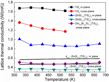
Table 1 Densities, longitudinal and transverse sound velocities and corresponding shear moduli of TiS2 and (SnS)1.2(TiS2)2 in the in-plane and cross-plane directions. For the cross-plane direction, the two transverse velocities are equal (VT1=VT2). In the in-plane direction, the polarization of VT1 is perpendicular and of VT2 is parallel to the layers.
Table 2 Debye temperatures of (SnS)1.2(TiS2)2 for each polarization in the in-plane and cross-plane directions.
In the cross-plane direction, kl of (SnS)1.2(TiS2)2 is even lower than kmin [Citation32], which can hardly be observed in the bulk materials. In the in-plane direction, the thermal conductivity reduction is mainly caused by the softening of the transverse phonons, and their polarization is normal to the layers due to weakened interlayer bonding. In the cross-plane direction, the reduction of thermal conductivity originates from both the decreased transverse velocity and phonon scattering enhanced by the modulated structure and translational disorder.
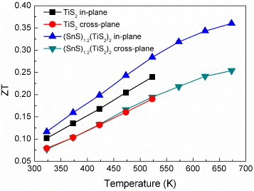
In the in-plane direction, the ZT value of (SnS)1.2(TiS2)2 is improved compared with TiS2 due to the superlattice structure (figure ) [Citation29], in which the phonon velocity is reduced without degrading the electrical properties. In the cross-plane direction, the ZT value is almost unchanged due to simultaneous scattering of both electrons and phonons at the heterointerfaces. Because (SnS)1.2(TiS2)2 have extremely low thermal conductivity and rather high carrier concentration, the reduction in carrier concentration can simultaneously lower the electronic thermal conductivity and optimize the power factor, thereby yielding a higher ZT value.
Figure 9 ZT values of TiS2 and (SnS)1.2(TiS2)2 in the in-plane and cross-plane directions.
Based on the example of (SnS)1.2(TiS2)2, we propose to vary the species of the host material and the intercalated material and the ratio of these two components. This will result in a large family of misfit layer compounds (MX)1+x(TX2)n having a natural superlattice structure, where M=Pb, Bi, Sn, Sb or a rare earth element; T=Ti, V, Cr, Nb or Ta, X=S or Se and n=1, 2, 3 [Citation33]. These compounds should exhibit superior thermoelectric properties both for n-type and p-type conductivity.
Conclusions
In the past decade, various strategies have been successfully developed to reduce the lattice thermal conductivities of thermoelectric materials with consequent enhancement of thermoelectric performance. The concept of minimum thermal conductivity should be reconsidered, as some experimental values are already beyond that limit. However, a further significant enhancement of the ZT value can only originate from a spectacular increase in the power factor (S2σ) that requires a breakthrough in the understanding and control of charge-transport mechanisms in complex materials.
References
- SnyderG JTobererE S 2008 Nat. Mater. 7 105 http://dx.doi.org/10.1038/nmat2090
- TobererE SMayA FSnyderG J 2010 Chem. Mater. 22 624 http://dx.doi.org/10.1021/cm901956r
- WoodC 1988 Rep. Prog. Phys. 51 459 http://dx.doi.org/10.1088/0034-4885/51/4/001
- ZaitsevV KFedorovM IGurievaE AEreminI SKonstantinovP PSamuninA YVedernikovM V 2006 Phys. Rev. B 74 045207 http://dx.doi.org/10.1103/PhysRevB.74.045207
- AbelesB 1963 Phys. Rev. 131 1906 http://dx.doi.org/10.1103/PhysRev.131.1906
- YuCScullinM LHuijbenMRameshRMajumdarA 2008 Appl. Phys. Lett. 92 191911 http://dx.doi.org/10.1063/1.2930679
- MayA FFleurialJ PSnyderG J 2008 Phys. Rev. B 78 125205 http://dx.doi.org/10.1103/PhysRevB.78.125205
- NolasG SWangDBeekmanM 2007 Phys. Rev. B 76
- WolfingBKlocCTeubnerJBucherE 2001 Phys. Rev. Lett. 86 4350 http://dx.doi.org/10.1103/PhysRevLett.86.4350
- YoshiyaMTadaMNagiraT 2007 Proc. Int. Symp. on Nano-Thermoelectrics p 49
- RhyeeJ SLeeK HLeeS MChoEIl KimSLeeEKwonY SShimJ HKotliarG 2009 Nature 459 965 http://dx.doi.org/10.1038/nature08088
- SalesB CMandrusDWilliamsR K 1996 Science 272 1325 http://dx.doi.org/10.1126/science.272.5266.1325
- CohnJ LNolasG SFessatidisVMetcalfT HSlackG A 1999 Phys. Rev. Lett. 82 779 http://dx.doi.org/10.1103/PhysRevLett.82.779
- ChungD YHoganTBrazisPRocci-LaneMKannewurfCBasteaMUherCKanatzidisM G 2000 Science 287 1024 http://dx.doi.org/10.1126/science.287.5455.1024
- KozaM MJohnsonM RViennoisRMutkaHGirardLRavotD 2008 Nat. Mater. 7 805 http://dx.doi.org/10.1038/nmat2260
- RoweD MShuklaV SSavvidesN 1981 Nature 290 765 http://dx.doi.org/10.1038/290765a0
- PoudelB et al 2008 Science 320 634 http://dx.doi.org/10.1126/science.1156446
- XieW JTangX FYanY GZhangQ JTrittT M 2009 Appl. Phys. Lett. 94 102111 http://dx.doi.org/10.1063/1.3097026
- LiebmannW KMillerE A 1963 J. Appl. Phys. 34 2653 http://dx.doi.org/10.1063/1.1729786
- ZhaoX BJiX HZhangY HZhuT JTuJ PZhangX B 2005 Appl. Phys. Lett. 86 062111 http://dx.doi.org/10.1063/1.1863440
- HochbaumA IChenR KDelgadoR DLiangW JGarnettE CNajarianMMajumdarAYangP D 2008 Nature 451 163 http://dx.doi.org/10.1038/nature06381
- KimWZideJGossardAKlenovDStemmerSShakouriAMajumdarA 2006 Phys. Rev. Lett. 96 045901 http://dx.doi.org/10.1103/PhysRevLett.96.045901
- AndroulakisJHsuK FPcionekRKongHUherCDAngeloJ JDowneyAHoganTKanatzidisM G 2006 Adv. Mater. 18 1170 http://dx.doi.org/10.1002/adma.200502770
- ZhouMLiJ FKitaT 2008 J. Am. Chem. Soc. 130 4527 http://dx.doi.org/10.1021/ja7110652
- ChiritescuCCahillD GNguyenNJohnsonDBodapatiAKeblinskiPZschackP 2007 Science 315 351 http://dx.doi.org/10.1126/science.1136494
- VenkatasubramanianRSiivolaEColpittsTO'QuinnB 2001 Nature 413 597 http://dx.doi.org/10.1038/35098012
- ChiritescuCCahillD GHeidemanCLinQ YMortensenCNguyenN TJohnsonDRostekRBottnerH 2008 J. Appl. Phys. 104 033533 http://dx.doi.org/10.1063/1.2967722
- BalandinAWangK L 1998 J. Appl. Phys. 84 6149–6153 http://dx.doi.org/10.1063/1.368928
- WanCWangYWangNKoumotoK J. Electron. Mater. submitted
- WanCWangYWangNKoumotoK 2010 Materials 3 2606 http://dx.doi.org/10.3390/ma3042606
- ImaiHShimakawaYKuboY 2001 Phys. Rev. B 64 241104 http://dx.doi.org/10.1103/PhysRevB.64.241104
- CahillD GWatsonS KPohlR O 1992 Phys. Rev. B 46 6131 http://dx.doi.org/10.1103/PhysRevB.46.6131
- WiegersG A 1996 Prog. Solid State Chem. 24 1 http://dx.doi.org/10.1016/0079-6786(95)00007-0
- ZengG HBahkJ HBowersJ ELuHGossardA CSingerS LMajumdarABianZ XZebarjadiMShakouriA 2009 Appl. Phys. Lett. 95 083503 http://dx.doi.org/10.1063/1.3213347