Abstract
We describe our recent experimental results on the fabrication of quantum-dot devices in a graphene-based two-dimensional system. Graphene samples were prepared by micromechanical cleavage of graphite crystals on a SiO2/Si substrate. We performed micro-Raman spectroscopy measurements to determine the number of layers of graphene flakes during the device fabrication process. By applying a nanofabrication process to the identified graphene flakes, we prepared a double-quantum-dot device structure comprising two lateral quantum dots coupled in series. Measurements of low-temperature electrical transport show the device to be a series-coupled double-dot system with varied interdot tunnel coupling, the strength of which changes continuously and non-monotonically as a function of gate voltage.
Introduction
The recent discovery of single-layer and multilayer graphenes has opened the door to a new area of low-dimensional physics [Citation1–3]. Their electronic properties are expected to differ from the well-studied 2-dimensional (2D) electron gas in a semiconductor heterostructure. The low-energy physics of graphene is described theoretically by (2+1)-dimensional Dirac fermions, where ‘2-dimensions’ corresponds to a graphite sheet and ‘1-dimension’ denotes time. The corresponding energy dispersion becomes the so-called Dirac cone, which leads to rich physics inherited from quantum electrodynamics.
In terms of applications, the 2D sheet structure of graphene and its properties of ballistic transport and high mobility make graphene a promising candidate for future quantum devices [Citation4] and even integrated quantum nanodevice systems. Graphene sheets can be carved out to form nanostructures such as quantum wires and quantum dots [Citation5–12]. Quantum dots are referred to as ‘artificial atoms’, in the sense that electrons are confined in a small space. They can be applied to novel quantum-dot devices, such as single-electron and quantum computing devices, which can control single-electron charge and spin states [Citation13–15]. Tunnel-coupled double-quantum-dot systems differ intrinsically from single-quantum-dot systems because of variable interdot tunnel coupling, and may eventually serve as the basic units of new logic and architectures for quantum computation and quantum cellular automata [Citation4, Citation14–17].
In this paper, we present a method of fabricating graphene-based quantum-dot devices and report an experimental demonstration of a tunnel-coupled double-quantum-dot device that exhibits single-electron transport of two lateral quantum dots coupled in series. The strength of interdot tunnel coupling varies continuously and non-monotonically as a function of gate voltage. Our fabrication method and transport results are important steps towards the realization of complex quantum-dot nanodevices.
Device fabrication
We prepared single-layer and multilayer graphene samples by micromechanical cleavage of graphite deposited on the surface of an oxidized Si substrate (thickness 290 nm). From these samples, we selected graphene flakes and determined the number of graphene layers therein. Optical microscope contrast and Raman spectroscopy measurements can generally be used to identify single-, double-, triple- and multilayer graphene flakes on a substrate. We selected graphene flakes using an optical microscope [Citation18] and observed them by Raman spectroscopy under ambient conditions at room temperature (laser spot size of ∼1 μm, lens objective of 90×). Samples were mounted on the precisely controllable x–y translation stage of a Raman microscope. The lateral resolution of the step position for Raman mapping measurements was 0.1 μm. The incident laser power was set to 1–2 mW on the sample for all measured wavelengths. No heating effects were observed in this range.
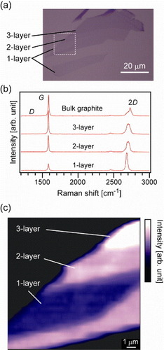
Figure (a) shows an optical microscope image of graphene flakes on a SiO2/Si substrate, and figure (b) shows Raman spectra of single-layer/multilayer graphene and bulk graphite (thickness of ∼200 nm, corresponding to >500 layers), obtained using the 514.5 nm (2.41 eV) laser line with the laser spot focused on the inner portion of the flakes. Raman spectroscopy is widely used to characterize carbon materials. In extending its use to graphene, we adopted the following notation: the band at ∼1580 cm−1 is the G band, that at ∼2700 cm−1 is the 2D band and, in the presence of elastic scattering, the band at ∼1350 cm−1 is the D band. The D band cannot be observed in the inner part of the sample, but only at its edge; spatially resolved spectroscopy is crucial for detecting it.
Figure 1 (a) Optical-microscope image of graphene flakes on a SiO2/Si substrate. (b) Raman spectra of graphene layers and bulk graphite. Spectra are shifted for clarity. (c) Raman mapping of the integrated intensity of the Raman G-band peak in the dashed square region in 1(a).
Based on previous studies of bulk graphite [Citation19, Citation20], we explain the Raman bands as follows. The G band is originates from the doubly degenerate zone-centre E2g mode, which involves a phonon with the highest energy at the Γ point in the Brillouin zone. The D/2D bands are caused by double resonance with one or two in-plane transverse optical (iTO) phonons close to the K point in the Brillouin zone [Citation19–21]. These bands reflect the electronic structure near the two nodes of the Dirac-cone energy dispersion [described as (2+1)-dimensional Dirac fermions] as well as phonon dispersion close to the K point. Other small peaks exist but are beyond the scope of this paper.
Before discussing the Raman D/2D bands, we first comment on how spatially resolved Raman spectroscopy works, focusing on the G band. As shown in figure (c), the G-band intensity increases with the number of layers (e.g. the intensity is higher for double-layer graphene than for single-layer graphene); we can use this fact to determine the number of layers in different regions. Figure (c) shows the integrated intensity of the G-band peak in the dashed square region in figure (a), which reveals the distribution of the number of layers in the window.
Let us next discuss the Raman D/2D bands. Figure shows these bands for different numbers of layers, with bulk graphite as a reference. The D-band peaks are observed not in the inner part of graphene-layer flakes but only at the section boundaries between the flakes and the SiO2 substrate, as revealed by spatially resolved Raman spectroscopy. These results indicate that defects and translational symmetry breaking are absent in the inner part of the measured flakes.
Figure 2 Raman spectra (514.5 nm) of different varieties of multilayer graphite and of reference bulk graphite. (a) D-band spectra; (b) 2D-band spectra. Spectra are shifted for clarity. Solid lines show Lorentzian functions that fit the experimental data.
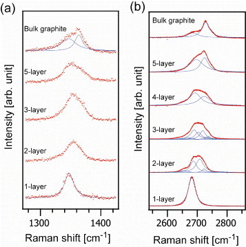
In figure (a), the D band has a maximum intensity at the section boundaries between flake and substrate, and we use this fact to examine D-band data. In figure (b), variations in the 2D band are clearly evident and are consistent with previous reports [Citation21–23]. For single-layer graphene, the 2D band can be fitted with a single Lorentzian peak. As discussed above, this band corresponds to inter-valley resonance with the emission of two phonons. For multilayer graphene, the situation becomes more complicated: For example, for double-layer graphene, the linear energy dispersion near the node splits into two, and four resonant scattering components appear, requiring four Lorentzian components in the 2D band; this phenomenon, shown in figure (b), is consistent with previous reports [Citation21, Citation23]. For more layers, subtle issues arise. As the number of layers increases, the number of peaks also increases, but some of the peaks merge and/or are strongly suppressed. In the limit of an infinite system of graphite layers, only two peaks are evident. Interestingly, for a tri-layer sample, we observed six peaks—from a symmetry point of view, the spectrum should consist of more peaks, but they are beyond our spectral resolution. Note that only two peaks are reported in [Citation23] because of the same problem. However, our result is consistent with more recent analysis and results in [Citation24].
Using these techniques, we confirmed that our samples shown here were triple-layer graphene (TLG) sheets.
To fabricate devices from the samples, we spin coated an 80 nm electron-beam (EB) resist (ZEP-520A) onto the samples. Then, using EB lithography, we patterned the desired device structure into the resist as an etch mask. Figure (a) shows a schematic top view of a sample designed to be a double-quantum-dot device. The green-coloured areas protect graphene under the resist. Figure (b) shows a schematic cross-sectional view of a sample during reactive ion etching (RIE). We used RIE based on oxygen plasma (power 50 W, base pressure 10 Pa) to etch away unprotected graphene. We then applied EB lithography (acceleration voltage 100 kV) to fabricate narrow openings (width 100 nm) in the resist layer. Finally, we again used EB lithography to deposit Cr/Au metal (thickness 10/50 nm) onto the TLG for the source–drain and side-gate contacts.
Figure 3 (a) Schematic top view of a sample designed to be a double-quantum-dot device. (b) Schematic cross-sectional view of a sample during reactive ion etching. (c) SEM image of a fabricated device with electrode and quantum-dot assignments. Bright areas show etched triple-layer graphene.
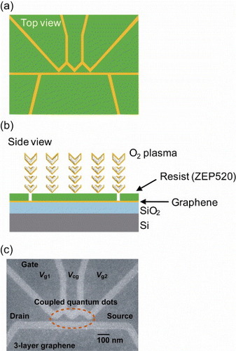
Figure (c) shows a scanning electron microscope (SEM) image of a fabricated TLG device [Citation11]. Highly p-doped Si substrate was used as a back gate (Vbg) and three lateral TLG side gates. The latter, labelled centre gate Vcg and gates Vg1(2), are expected to couple to the individual dot 1(2). The dots are triangular in shape (dot 1: area S1 ≈ 0.004 μm2; dot 2: S2 ≈ 0.005 μm2), connected by a narrow constriction (length 20 nm, width 15 nm) that is expected to act as a tunnel barrier owing to the quantum-size effect.
Electrical properties
To measure the electrical properties of the fabricated TLG double-quantum-dot devices, we placed the samples in a dilution refrigerator. All electrical transport measurements were carried out at a base temperature of 30 mK and electron temperature of ∼240 mK, allowing us to use the results for one sample as a reference for the other under the same measurement conditions [Citation25]. We measured the dc current I through a device by applying dc bias voltage Vsd with a dc voltage source and current amplifier.
To form a double-quantum-dot system, we used previous results [Citation11], with Vbg fixed at 4.0 V, which is approximately the charge-neutrality point, and Vcg fixed at 9.0 V, near the current-suppression region. Figure (a) shows the equivalent circuit diagram for a double-quantum-dot system. The system can be controlled by adjusting Vsd and gate voltages Vg1 and Vg2, which are capacitively coupled to each dot. Figure (b) shows a charge stability diagram of the system [Citation26], where (n, m) pairs indicate the excess charges in dots 1 and 2. Inside the hexagonal lattices, the number of charges on the two dots is constant in the Coulomb blockade regime, so no current flows. Resonant current flows at the vertices where the charge states in the double-quantum dots are degenerate, the so-called triple points, indicated by black dots in the figure. Off-resonant tunnelling may occur when the energy levels of a dot align with neighbouring leads. This so-called co-tunnelling occurs at the edge of the hexagonal lattices indicated by dashed lines in the figure.
Figure 4 Double-quantum-dot system. (a) Equivalent circuit diagram, (b) charge stability diagram where (n, m) indicates the excess charges in dots 1 and 2. Resonant current flows at the vertices of the hexagonal lattice (black dots), and co-tunnelling current flows along the edge of the hexagonal lattice (dashed lines). (c) Colour-scale plot of current I through the system as a function of Vg1 and Vg2 at fixed Vbg=4.0 V, Vcg=9.0 V and Vsd=800 μV. Current was measured as a function of Vg1 with stepwise variation of Vg2.
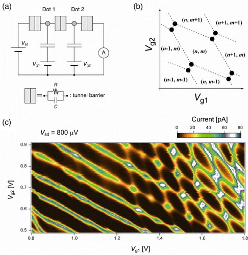
Figure (c) shows a colour-scale plot of current I through the system as a function of Vg1 and Vg2, with applied bias voltage Vsd=800 μV. In the range Vg1 >1.5 V, hexagonal patterns are clearly evident. Current along all hexagon boundaries is finite, indicating that the system is in a strongly coupled regime, and the two dots interact by quantum-mechanical tunnel coupling, analogous to coupling by covalent bonding in a two-atom molecule [Citation27–29].
The honeycomb structures vary with gate voltage. In the middle range 1.25 V <Vg1 < 1.5 V, the triple points move closer together and the hexagons become squares. In the range Vg1 < 1.25 V, current oscillates as a function of Vg1 or Vg2. In the dark-brown regions between arrays of current peaks, the current is completely suppressed. These results indicate that interdot coupling can be controlled by varying Vg1 and Vg2, because the side gates affect the central barrier through the existing capacitances between the side gates and the central barrier [Citation30]. Thus, in the range Vg1 <1.25 V, a double-quantum-dot system behaves as a single-quantum-dot system, and in the range 1.25 V <Vg1 < 1.5 V, the two dots are in a weak electrostatic coupling regime [Citation26]. Interdot coupling changes continuously and non-monotonically as a function of gate voltages Vg1 and Vg2 in our measured device. In addition, coupling may occur between dot 1 (2) and the adjacent lead. Similar behaviours have been reported in graphene double-quantum dots, graphene nanoribbons and graphene nanoconstrictions [Citation10–12, Citation31–34]. These effects may originate from disorder near the narrow constrictions, both lead-to-dot and dot-to-dot, but this is not clear at the moment, and needs to be investigated further.
Conclusions
We fabricated quantum-dot devices in graphene-based two-dimensional materials and measured their electrical transport properties. We determined the fine details of graphene layers on a SiO2/Si substrate from their Raman fingerprint and fabricated double-quantum-dot devices with the identified graphene flakes. The coupled quantum-dot formation has been confirmed by observation of the charge stability diagrams showing variable interdot tunnel coupling that changes continuously and non-monotonically as a function of gate voltages. Although our fabrication method enables precise control of device structure on a submicron scale, the edge shape varies on an atomic scale, and these structural fluctuations are likely to affect tunnel-barrier formation and electron transport through the narrow constrictions between the source–drain electrodes and quantum dots. Further optimization and control of edge states in graphene are necessary to realize reliable quantum-dot devices.
Acknowledgments
We thank Taketoshi Fujita of MANA for technical support with the Raman spectroscopy measurements. This work was supported in part by the following: Nanotechnology Network Program, Grant-in-Aid for Exploratory Research (22656024), Grant-in-Aid for Scientific Research (B) (22360147), Grant-in-Aid for Young Scientists (B) (22740248) and the World Premier International Research Center (WPI) Initiative on Materials Nanoarchitectonics from the Ministry of Education, Culture, Sports, Science and Technology, Japan.
References
- NovoselovK SGeimA KMorozovS VJiangDZhangYDubonosS VGrigorievaI VFirsovA A 2004 Science 306 666 http://dx.doi.org/10.1126/science.1102896
- NovoselovK SGeimA KMorozovS VJiangDKatsnelsonM IGrigorievaI VDubonosS VFirsovA A 2005 Nature 438 197 http://dx.doi.org/10.1038/nature04233
- ZhangYTanY-WStormerH LKimP 2005 Nature 438 201 http://dx.doi.org/10.1038/nature04235
- TrauzettelBBulaevD VLossDBurkardD 2007 Nat. Phys. 3 192 http://dx.doi.org/10.1038/nphys544
- HanM YÖzyilmazBZhangYKimP 2007 Phys. Rev. Lett. 98 206805 http://dx.doi.org/10.1103/PhysRevLett.98.206805
- SolsFGuineaFCastro NetoA H 2007 Phys. Rev. Lett. 99 166803 http://dx.doi.org/10.1103/PhysRevLett.99.166803
- StampferCSchurtenbergerEMolitorFGüttingerJIhnTEnsslinK 2008 Nano Lett. 8 2378 http://dx.doi.org/10.1021/nl801225h
- PonomarenkoL ASchedinFKatsnelsonM IYangRHillE WNovoselovK SGeimA K 2008 Science 320 356 http://dx.doi.org/10.1126/science.1154663
- GüttingerJStampferCMolitorFGrafDIhnTEnsslinK 2008 New J. Phys. 10 125029 http://dx.doi.org/10.1088/1367-2630/10/12/125029
- MolitorFDröscherSGüttingerJJacobsenAStampferCIhnTEnsslinK 2009 Appl. Phys. Lett. 94 222107 http://dx.doi.org/10.1063/1.3148367
- MoriyamaSTsuyaDWatanabeEUjiSShimizuMMoriTYamaguchiTIshibashiK 2009 Nano Lett. 9 2891 http://dx.doi.org/10.1021/nl9011535
- LiuX LHugDVandersypenL M K 2010 Nano Lett. 10 1623 http://dx.doi.org/10.1021/nl9040912
- GrabertHDevoretM H 1991 Single Charge Tunneling New York Plenum
- BarenceADeutschDEkertAJozsaR 1995 Phys. Rev. Lett. 74 4083 http://dx.doi.org/10.1103/PhysRevLett.74.4083
- HansonRKouwenhovenL PPetaJ RTaruchaSVandersypenL M K 2007 Rev. Mod. Phys. 79 1217 http://dx.doi.org/10.1103/RevModPhys.79.1217
- IshibashiKMoriyamaSFuseT 2004 IEICE Trans. Electron. E 87 1799
- LentC STougawP DPorodW 1993 Appl. Phys. Lett. 62 714 http://dx.doi.org/10.1063/1.108848
- BlakePHillE WCastroNetoNovoselovK SJiangDYangRBoothT JGeimA K 2007 Appl. Phys. Lett. 91 063124 http://dx.doi.org/10.1063/1.2768624
- ThomsenCReichS 2000 Phys. Rev. Lett. 85 5214 http://dx.doi.org/10.1103/PhysRevLett.85.5214
- ReichSThomsenC 2004 Phil. Trans. R. Soc. A 362 2271 http://dx.doi.org/10.1098/rsta.2004.1454
- FerrariA C et al 2006 Phys. Rev. Lett. 97 187401 http://dx.doi.org/10.1103/PhysRevLett.97.187401
- GuptaAChenGJoshiPTadigadapaSEklundP C 2006 Nano Lett. 6 2667 http://dx.doi.org/10.1021/nl061420a
- GrafDMolitorFEnsslinKStampferCJungenAHieroldCWirtzL 2007 Nano Lett. 7 238 http://dx.doi.org/10.1021/nl061702a
- MalardL MGuimaräesM H DMafraD LMazzoniM S CJorioA 2009 Phys. Rev. B 79 125426 http://dx.doi.org/10.1103/PhysRevB.79.125426
- MoriyamaSFuseTSuzukiMAoyagiYIshibashiK 2005 Phys. Rev. Lett. 94 186806 http://dx.doi.org/10.1103/PhysRevLett.94.186806
- van der WielW GFanceschiS DeElzermanJ MFujisawaTTaruchaSKouwenhovenL P 2003 Rev. Mod. Phys. 75 1 http://dx.doi.org/10.1103/RevModPhys.75.1
- SapmazSMeyerCBeliczynskiPJarillo-HerreroPKouwenhovenL P 2006 Nano Lett. 6 1350 http://dx.doi.org/10.1021/nl052498e
- GräberM RCoishW AHoffmannCWeissMFurerJOberholzerSLossDSchönenbergerC 2006 Phys. Rev. B 74 075427 http://dx.doi.org/10.1103/PhysRevB.74.075427
- J⊘rgensenH IGrove-RasmussenKWangK-YBlackburnA MFlensbergKLindelofP EWilliamsD A 2008 Nat. Phys. 4 536 http://dx.doi.org/10.1038/nphys987
- IshibashiKSuzukiMMoriyamaSIdaTAoyagiY 2002 Superlattices Microstruct. 31 141 http://dx.doi.org/10.1006/spmi.2002.1035
- MolitorF et al 2010 Europhys. Lett. 89 67005 http://dx.doi.org/10.1209/0295-5075/89/67005
- StampferCGüttingerJHellmülerSMolitorFEnsslinKIhnT 2009 Phys. Rev. Lett. 102 056403 http://dx.doi.org/10.1103/PhysRevLett.102.056403
- MolitorFJacobsenAStampferCGüttingerJIhnTEnsslinK 2009 Phys. Rev. B 79 075426 http://dx.doi.org/10.1103/PhysRevB.79.075426
- ToddKChouH-TAmashaSGoldhaber-GordonD 2009 Nano Lett. 9 416 http://dx.doi.org/10.1021/nl803291b