Abstract
Atomic switches are nanoionic devices that control the diffusion of metal cations and their reduction/oxidation processes in the switching operation to form/annihilate a metal atomic bridge, which is a conductive path between two electrodes in the on-state. In contrast to conventional semiconductor devices, atomic switches can provide a highly conductive channel even if their size is of nanometer order. In addition to their small size and low on-resistance, their nonvolatility has enabled the development of new types of programmable devices, which may achieve all the required functions on a single chip. Three-terminal atomic switches have also been developed, in which the formation and annihilation of a metal atomic bridge between a source electrode and a drain electrode are controlled by a third (gate) electrode. Three-terminal atomic switches are expected to enhance the development of new types of logic circuits, such as nonvolatile logic. The recent development of atomic switches that use a metal oxide as the ionic conductive material has enabled the integration of atomic switches with complementary metal-oxide-semiconductor (CMOS) devices, which will facilitate the commercialization of atomic switches. The novel characteristics of atomic switches, such as their learning and photosensing abilities, are also introduced in the latter part of this review.
Introduction
Over the past several decades, information technology has developed in an evolutionary manner, supported by the continuous downsizing of semiconductor devices. As Moore predicted, the number of transistors on an integrated circuit has doubled approximately every two years [Citation1]. The consequent and continuing CMOS scaling has exponentially decreased the minimum feature size used in integrated circuits [Citation2]. However, now that sizes are about to reach the atomic scale, the physical, technological and economic limitations of CMOS technologies are in turn presenting significant challenges for further development. This situation has driven us to develop new devices that have novel functions and can be integrated into the CMOS platform (‘more than Moore’) or that have completely different operational principles beyond current CMOS devices (‘beyond CMOS’).
A number of devices that target more than Moore and beyond CMOS functionalities have been proposed so far [Citation3–11]. Among these, ionic devices utilizing local ion transport have attracted significant attention as components that can extend or replace CMOS technology [Citation2, Citation12]. They include two types of devices depending on the polarity of ions contributing to forming conduction paths, i.e. anions or cations. Anion-based ionic devices contain one of the resistive random access memories (ReRAMs), consisting of a metal oxide layer sandwiched by two inert metal electrodes [Citation2]. For example, in Pt/TiO2/Pt [Citation13] and Pt/NiO/Pt [Citation14] systems, changes in resistance are caused by local oxidation/reduction of the metal oxide layers by oxygen vacancies [Citation12]. In cation-based ionic devices such as Ag/Ag2S/Pt [Citation15] and Cu/Ta2O5/Pt [Citation16], one of the electrodes can reversibly supply/incorporate metal cations into/from an ionic conductor sandwiched by two metal electrodes. In operation, metal atoms yielded by the reduction of metal cations form a conductive channel in or on the ionic conductor [Citation15–19]. Since metal cations/atoms are responsible for the switching operation in such cation-based ionic devices, they are also referred to as atomic switches [Citation2]. Here, we provide a comprehensive review of the research on atomic switches, including recent results of the studies from fundamentals to applications.
Control of atomic movement using STM
The concept of an atomic switch was introduced by Eigler et al in 1991 [Citation20]. They demonstrated resistive switching by controlling the transfer of atoms between the tip of a scanning tunneling microscope (STM) and a sample surface. The resistance changed by one order of magnitude depending on the adsorption site of the transferred atoms. The STM also enabled stepwise changes in the conductance (n×2e2/h) by moving the tip position to control the atomic contact formed between the tip and the sample [Citation21]. This ‘mechanically’ controlled atomic switch has attracted considerable attention, resulting in the development of ‘electrically’ controlled nanoscale atomic switches. Hereafter in this review, ‘atomic switches’ refer to cation-based ionic devices.
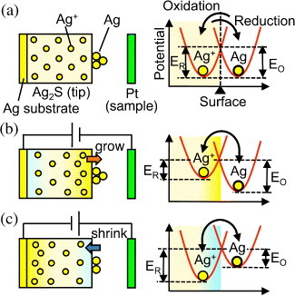
The key phenomenon in atomic switch operation is the formation and annihilation of metal filaments using a solid electrochemical reaction. For instance, electron injection into a Ag2S crystal, which is a mixed ionic- and electronic-conductor, causes the reduction of Ag+ cations () and the precipitation of Ag atoms on the surface of the Ag2S crystal [Citation22]. Figure shows a Ag protrusion grown on a Ag2S STM tip, where tunneling electrons caused the precipitation [Citation23]. The STM operation also enables the shrinkage of the grown Ag protrusion by changing the polarity of the bias voltage. Consequently, the STM makes it possible to control the growth and shrinkage of a Ag protrusion through the application of an appropriate bias voltage and tunneling current. Figure shows such controlled growth and shrinkage of a Ag protrusion, which grew when Vs (bias voltage applied to the sample) =−2.0 V and It (tunneling current) =1.35 nA (condition 2), and shrank when Vs=+2.0 V and It=0.35 nA (condition 4). However, no growth and shrinkage were observed under low-current conditions such as condition 1 and 3, which means that the growth and shrinkage have a threshold current. These phenomena can be explained as follows. Under the equilibrium condition, without the application of a bias voltage, the Ag substrate behind the Ag2S tip maintains the equal electrochemical potential of Ag+ cations in the Ag2S tip and Ag atoms on the tip surface. Consequently, the activation energies of reduction (ER; Ag+→ Ag) and oxidation (EO; Ag→ Ag+) at the surface are equal, as shown in figure (a). The application of a positive bias voltage to the Ag2S tip stimulates the diffusion of Ag+ cations toward the tip surface, which increases the concentration of Ag+ cations at the subsurface, as schematically shown in figure (b). Since the electrochemical potential is expressed as μ=μ0+Fφ+RTln γC (μ0 is the chemical potential at γC=1;F, φ, R, T, γ and C are the Faraday constant, electrical potential, molar gas constant, temperature, activity coefficient and concentration of the metal cation, respectively) [Citation24], the electrochemical potential of the Ag+ cations increases owing to the increase in concentration C. As a result, ER becomes smaller than EO, promoting the reduction process. On the other hand, applying a negative bias voltage to the Ag2S electrode induces the migration of Ag+ cations towards the bottom of the Ag2S tip, leading to a decrease in Ag+ concentration at the subsurface. Consequently, EO becomes smaller than ER, promoting the oxidation and shrinkage of the Ag protrusion.
Figure 1 Scanning electron microscopy (SEM) image of a Ag protrusion grown during an experiment. (Reproduced with permission from [Citation23] ©2002 AIP.)
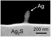
Figure 2 STM-controlled growth and shrinkage of a Ag protrusion on the surface of a Ag2S crystal. (Reproduced with permission from [Citation23] ©2002 AIP.)
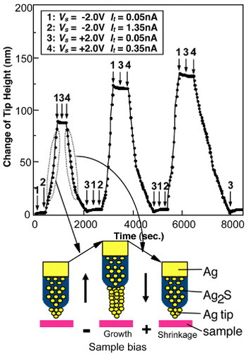
Figure 3 Mechanisms of Ag wire growth and shrinkage: (a) the activation energies for reduction (ER) and oxidation (EO) are equal at zero bias. (b) ER becomes smaller than EO when a positive bias is applied to the Ag2S tip, and Ag+ cations in the tip are reduced, leading to the growth of a Ag protrusion (growth mechanism). (c) EO becomes smaller than ER when a negative bias is applied, and Ag atoms in the protrusion are oxidized to Ag+ cations, which diffuse into the Ag2S tip (shrinkage mechanism).
Under a quasi-equilibrium condition, where the application of bias voltage induces an electric field both in the Ag2S tip and in the tunneling gap, the concentration of Ag+ cations has a distribution that equalizes the electrochemical potential everywhere in the Ag2S tip, thus compensating for any changes in electrical potential. Since the concentration at the bottom of the Ag2S tip is fixed by the Ag substrate, which serves as a reservoir of Ag atoms, the concentration at the surface increases by a factor of (1/γ)×exp (FVAg2S/RT). Here, VAg2S is the effective bias voltage at the Ag2S tip and is determined by the product RAg2S ×It, where RAg2S is the resistance of the Ag2S tip and It is the tunneling current. As a result, the electrochemical potential of Ag+ at the surface increases by a factor of FVAg2S=FRAg2S ×It. In other words, the activation energy for reduction decreases linearly with It. This is why the growth rate of the Ag protrusion (dl/dt) exponentially depends on It rather than on V [Citation23], as expressed by equation
Here, E is the activation energy, kB is the Boltzmann constant, T is the temperature, and A and D are constants. This also explains the exponential dependence of the shrinkage rate on It. Differences in the derivative of the growth and shrinkage rates yield different coefficients, i.e. Ds for shrinkage and Dg for growth [Citation23]. This difference is mainly caused by changes in the concentration of Ag+ cations at the surface. Since Ag2S is an n-type semiconductor, increasing the number of Ag+ cations is energetically easier than decreasing it.
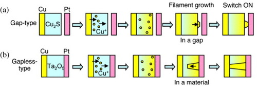
Gap-type atomic switches
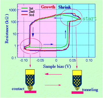
The STM-controlled growth and shrinkage of Ag protrusions led to the first demonstration of atomic switch operations [Citation17], where the Ag2S tip position was fixed about 1 nm above a Pt surface by disabling the STM feedback control. When a negative bias was applied to the Pt sample, a Ag protrusion grew to a length of about 1 nm, equivalent to the gap size, to bridge the gap between the Ag2S tip and the Pt sample. When a positive bias was applied to the sample, the Ag protrusion shrank to restore the gap between both electrodes, as shown in figure . Consequently, bipolar switching was demonstrated by sweeping the bias voltage applied to the Pt sample from positive to negative and vice versa. Figure shows how such bipolar switching was conducted in a bias-sweeping experiment, where the application of a negative bias voltage to the Pt sample caused the precipitation of Ag atoms and the formation of a bridge. In contrast, the application of a positive bias voltage caused the oxidation of the precipitated Ag atoms and the disappearance of the bridge. Although only three cycles of this bipolar switching are shown in figure , 105 cycles were achieved in actual experiments [Citation18].
Figure 4 Atomic switch operation controlled by STM: (a) disabling the STM feedback control maintains a gap of about 1 nm between the Ag2S tip and the Pt sample. When a negative bias is applied to the Pt sample, a Ag protrusion grows to a length of about 1 nm to bridge the gap. (b) When a positive bias is applied to the sample, the protrusion shrinks, restoring the gap between the tip and the sample.
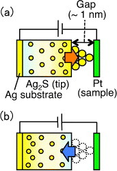
Figure 5 Bipolar switching of the atomic bridge formed between the Ag2S tip and the Pt sample. (Reproduced with permission from [Citation17] ©2001 RIKEN.)
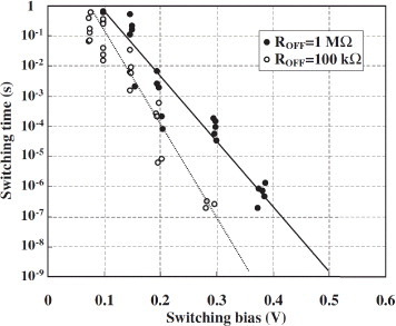
Switching by the application of bipolar biases, such as ±600 mV at 1 MHz, was also achieved in a gap-type atomic switch with a crossbar structure (described below) as shown in figure , in which the resistance changed between 100 and 2 kΩ [Citation18]. The dependence of the switching time on the bias voltage is shown in figure [Citation25]. The switching time was taken as the time required for the resistance to decrease from the off value (1 MΩ or 100 kΩ) to 12.9 kΩ, known as the resistance of a single atomic contact [Citation26, Citation27]. As expected from the operating mechanism, involving a solid electrochemical reaction with a certain activation energy, the switching time decreases exponentially as the switching bias voltage increases. A recent study has revealed that the switching time is described by the following equation [Citation28]:
where Ea is the activation energy for the reduction/oxidation processes, D is a constant, V is the switching bias voltage, kB is the Boltzmann constant and T is the temperature. While tunneling current (It) is the variable in the controlled growth and shrinkage (equation (1), bias voltage (V) is the variable in equation (2). This is because the tunneling current changes during the switching operation owing to the growth of the Ag protrusion and cannot be preset externally. However, it should be noted that V grows linearly with It as V=It×(Rgap+RAg2S) and that the bias voltage dependence of the switching time has the same origin as that of the growth and shrinkage rates.
Figure 6 Experimental trace of 1 MHz operation of a gap-type atomic switch with a crossbar structure. An alternating switching bias of ±600 mV was applied. (Reproduced with permission from [Citation18] ©2005 NPG.)
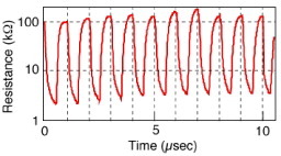
Figure 7 Switching time dependence on switching bias voltage and initial off resistance in the gap-type atomic switch, measured in an STM setup. (Reproduced with permission from [Citation25] ©2006 JSAP.)
The temperature dependence of the switching time has revealed that more than one rate-limiting process determines the switching time [Citation29]. When the switching bias voltage is below 0.2 V, the reduction process is rate limiting and the activation energy is 0.5 eV. On the other hand, the diffusion of Ag+ cations is rate limiting when the switching bias voltage exceeds 0.2 V, and the activation energy is about 1.3 eV. Switching has also been demonstrated using Cu2S [Citation28], which exhibits a similar bias voltage dependence.
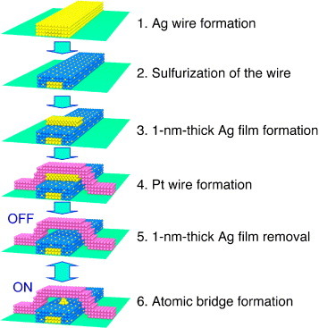
Atomic switch operations were demonstrated using an STM at the beginning of their development. Later, a fabrication method for a gap-type atomic switch with a crossbar structure was developed using conventional miniaturization techniques [Citation18]. A 1 nm gap between Ag2S and Pt electrodes is formed by a solid electrochemical reaction after the fabrication of the device structure in the on-state. The fabrication process is shown schematically in figure . A Ag nanowire is formed on an insulator, the surface of the Ag nanowire is sulfurized, and a 1-nm-thick Ag film is then deposited on the Ag2S-covered Ag nanowire at the position where the wire crosses the Pt wire. Pt deposition to form the crossing nanowire completes the fabrication process. The application of a positive bias voltage to the Pt nanowire converts Ag atoms to Ag+ cations, which are incorporated into the Ag2S layer. Then, the 1 nm gap appears, and the switch is in the off-state. The introduction of this fabrication method has enabled the demonstration of basic circuits [Citation18], such as logic gates, consisting of several atomic switches and other elements, which will be discussed in the following section.
Figure 8 Process for fabricating a gap-type atomic switch with a crossbar structure using conventional miniaturization techniques.
Advanced atomic switches
Gapless-type atomic switches
A gapless two-terminal atomic switch (figure ) consists of a metal/ionic conductor/metal (MIM) structure, where one of the metals (M1) should be electrochemically active and the other (M2) should be electrochemically inert. When a positive bias voltage is applied to the M1 electrode, its atoms dissolve in the ionic conductor. The dissolved metal cations (M1+) migrate towards the inert electrode (M2), where they are reduced to form a metal filament that grows toward the M1 electrode. A bias voltage of the opposite polarity oxidizes the metal atoms in the filament and causes them to redissolve. Consequently, the filament disappears, turning the switch off. The operating mechanisms for both gapless-type and gap-type atomic switches are schematically shown in figure . The difference between gapless-type and gap-type atomic switches is that, in the former, there is no gap between the ionic conductor and the inert metal electrode, which acts as a blocking electrode, resulting in the formation of a metal filament in the ionic conductor. The switching operation has been confirmed for Cu2S [Citation19, Citation30], Ag2S [Citation31, Citation32], Ag–Ge–Se [Citation33], Ge0.2S0.8 [Citation34], Ta2O5 [Citation16], HfO2 [Citation35] and AgI [Citation36].
Figure 9 Schematic diagram of a gapless-type atomic switch. A filament of metal M1 is formed in the ionic conductive material (I).
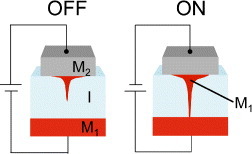
Figure 10 Operation mechanisms of (a) gap-type and (b) gapless-type atomic switches.
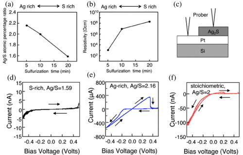
Gapless-type atomic switches can be configured without an active electrode when an ionic conductive material contains sufficient cations, which form metal filaments in the material. Kundu et al investigated the switching properties of Ag2S [Citation31] and Cu2S [Citation30] atomic switches with respect to their stoichiometries, i.e. the cation (Ag or Cu) to sulfur ratio. The stoichiometry depended on the sulfurization conditions of the ionic conductive materials. For instance, S-rich (Ag/S=1.59), stoichiometric (Ag/S=2) and Ag-rich (Ag/S=2.16) films were grown by changing the sulfurization conditions as shown in figure . Resistivity increased from the Ag-rich to S-rich films, as expected for an n-type Ag2S semiconductor [Citation24]. Electrical measurement using the two-point probe method illustrated in figure (c) revealed good switching properties only in the Ag-rich film. This can be explained as follows. The precipitation of Ag atoms at the interface of Pt and Ag2S needs the supersaturation of Ag+ cations in the Ag2S film. Since we used a tungsten probe in the experiment, there was no additional supply of Ag+ cations into the Ag2S film. Therefore, there were too few Ag+ cations to cause supersaturation in the S-rich and stoichiometric films.
Figure 11 Properties of a gapless Ag2S atomic switch. Only the Ag-rich Ag2S film exhibited good switching characteristics. (Reproduced with permission from [Citation31] ©2006 AIP.)
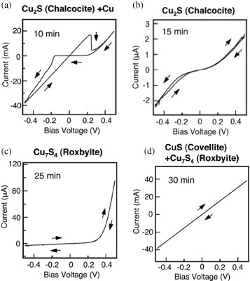
The effect of the sulfurization conditions on the structural and electrical properties has been examined for Cu2S films with various crystal phases, such as mixed-metallic Cu-chalcocite, chalcocite, roxbyite and roxbyite-covellite [Citation30]. The Cu/S atomic ratio of the films decreased with increasing sulfurization time, resulting in Cu-rich, stoichiometric (Cu2S with underlying unreacted Cu), pure stoichiometric and then S-rich films. Similarly to the results for Ag2S films, only the Cu-rich film (Cu-chalcocite) exhibited good switching properties, as shown in figure . The results for Cu2S films also suggest that the supersaturation of metal cations initiates metal filament growth, turning the switch on. Therefore, a well-functioning atomic switch can be prepared using a chalcogenide film formed on a metal electrode that can supply metal cations into the chalcogenide film.
Figure 12 Properties of a gapless Cu2S atomic switch. Only the Cu-rich Cu2S film exhibited good switching characteristics. (Reproduced with permission from [Citation30] ©2008 AIP.)
Recently, gapless-type atomic switches with metal oxides as an ionic conductor have been developed [Citation16], which has accelerated the development of atomic switches for commercialization [Citation37]. In most cases, metal oxides do not contain metal cations that diffuse and form a metal filament in the materials. Consequently, one of the electrodes should be an active electrode. The operating mechanism of these metal-oxide atomic switches has been investigated extensively, revealing that metal filament formation and annihilation are essential for the switching phenomena [Citation38]. Joule heating also has an important role in the turning off process, i.e. the annihilation of the metal filament.
In the operation of a gapless-type atomic switch, a conductive path should be formed between both ends of an ionic conductive material, meaning that the length of the conductive path must be almost equal to the thickness of the ionic conductive layer. Since the thickness is usually greater than a few nanometers, the switching time, particularly in the first switching operation called the ‘forming process’, should depend on the cation diffusion constant [Citation39, Citation40]. A higher bias voltage is usually required in the forming process than in the subsequent cycles. After the forming, switching is thought to occur through the formation and annihilation of a nanoscale metal filament, as in gap-type atomic switches. A very short switching time of 5 ns has been reported for metal oxides [Citation41, Citation42].
Gapless-type atomic switch operation has been demonstrated using various metal oxides, as shown in table . The wide range of switching bias voltages enables the selective use of materials depending on the application. The typical on-resistance is 100 Ω–1 kΩ and the off-resistance is 1 MΩ–1 GΩ, depending on the material and the operating conditions. Thus, the on/off ratio varies between 103 and 107. A lifetime of 1011 cycles [Citation43] and a retention time of 10 years [Citation44] have been reported.
Switching bias voltages of various gapless-type atomic switches.
Three-terminal atomic switches
In electrochemistry, controlling the reduction and oxidation in an electrolyte (solution) by using a gate electrode is a conventional technique. This technique makes it possible to control the formation and annihilation of a metal filament between two Au electrodes in a AgNO3+HNO3 electrolyte, as illustrated in figure (a) [Citation45]. Precise control of the gate voltage leads to switching among the quantized conductances. In other words, one can manipulate the number of atoms forming a point contact [Citation46].
Figure 13 Three-terminal atomic switches: atomic bridge formation (a) in electrolyte solution and (b) in solid electrolyte.
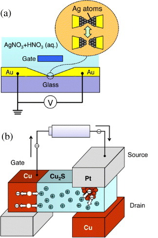
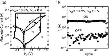
Recently, a similar operation has been achieved in a solid electrolyte using Cu2S [Citation47]. Cu bridge formation and annihilation between the source electrode (Pt) and drain electrode (Cu) were controlled by a gate electrode (Cu), as illustrated in figure (b). When a positive bias voltage was applied to the gate electrode, Cu+ cations were supplied into the Cu2S from the gate electrode by the oxidation of Cu atoms at the surface of the gate electrode. Cu+ cations migrated towards the source and drain electrodes, where they were reduced to form a conductive atomic bridge between the electrodes. When a negative bias voltage was applied to the gate electrode, Cu atoms were extracted from the atomic bridge as a result of their oxidation to Cu+ cations. The atomic bridge then became thinner and eventually disappeared, turning off the switch. Here, the arrangement of the three electrodes should be designed carefully to avoid a metal filament forming between the gate electrode and the other two electrodes. The initialization process, in which an atomic copper bridge is formed between the source and drain electrodes by using the electrodes as a two-terminal atomic switch, is helpful in reducing the effective distance between the source and drain electrodes. Sakamoto et al [Citation48] used a Cu drain electrode for this initialization process. The operating characteristics of the three-terminal atomic switch using Cu2S are shown in figure , where the drain current (ID) increased at a gate voltage (VG) of 0.22 V and decreased at VG=−0.13 V. In the operation, on-resistance and off-resistance were estimated to be on the order of 100 Ω and 100 MΩ, respectively. Consequently, the on/off ratio was about 106. Recently, three-terminal atomic switches based on metal filament formation and annihilation have been integrated into the metal layers of CMOS devices [Citation48] to be used as programmable switches.
Figure 14 Operating characteristics of a three-terminal atomic switch using a solid electrolyte. (Reproduced with permission from [Citation47] ©2006 IEICE.)
Memristors
A passive two-terminal device named a memristor was predicted by Chua in a theoretical study of symmetries in electrical devices and circuits [Citation49]. ‘Memristor’ is an abbreviation of ‘memory resistor’, i.e. a resistor having a memory effect. One of the operation modes of the memristor can be expressed as follows:
where ROFF/RON are the resistances in the off/on states, respectively, μV is the average ion mobility and D is the thickness of an ion conductive layer sandwiched by two electrodes. Therefore, memresistance M(q) is a function of the time-dependent charge q.
Although similar operations were achieved in commercialized devices over 30 years ago [Citation50], the memristor has attracted significant attention only recently [Citation51] because of the approaching ultimate scaling limit of CMOS devices [Citation2]. A recent demonstration of the memristor was achieved using TiO2 as the ionic conductive material sandwiched by Pt and Ti electrodes [Citation52]. Oxygen vacancies are considered to be responsible for the operation of this TiO2 memristor, meaning that this memristive operation was realized using ReRAM technology.
Memristive operation can also be achieved using gapless-type atomic switch technology, in which cations are controlled in an ion conductive material. The ‘memoriode’, which was developed in the 1970s, is an example of memristive operation based on atomic switches. Here, ‘memoriode’ refers to a device (-ode) having a memory effect. The operating characteristics described by equation (3) have been demonstrated in an atomic-switch-based memristor [Citation50], where changes in resistance of a Ag/solid electrolyte/AgX system were controlled by increasing/decreasing the concentration of Ag cations in AgX, and Ag was deposited on the Au electrode in the solid electrolyte. Since the amount of Ag deposition, i.e. the resistance of the system, is a function of the total coulomb current, the system was named a ‘couliode’. A key point of the memristor is that its operating parameter is not bias but integrated current [Citation51], which is the cause of the memory effect. Because of this effect, memristors can also act as a multistate memory.
Gap-type atomic switches also act as memristors [Citation53], in which the height of the grown protrusion is the operating parameter. Since the resistance of gap-type atomic switches is determined by the height and thickness of the protrusion, gap-type atomic switches, which can store information inside a solid electrolyte electrode, exhibit novel characteristics as discussed in section 4.5.
Photo-assisted atomic switches
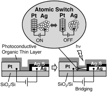
Atomic switches require a small amount of electrons to induce the reduction/oxidation of metal cations/atoms. That is why a gap-type atomic switch requires a nanogap between its two electrodes, which may require a complicated fabrication process. A photo-assisted atomic switch, which does not require a narrow nanogap, has recently been developed [Citation54]. In the photo-assisted atomic switch, a photoconductive material is introduced in a wider nanogap (several tens of nm) between an ion- and electron-conducting electrode and a counter metal electrode, as shown in figure . Light generates a photocurrent between the two biased electrodes, resulting in the growth of a metal filament from the ion- and electron-conducting electrode. The photo-assisted atomic switch is turned on when the growing metal filament reaches the counter electrode. Since the filament does not grow in the dark, the photo-assisted atomic switch acts as a programmable switch, such as that used in an erasable programmable read-only memory (EPROM).
Figure 15 Schematic diagram of a photo-assisted atomic switch. (Reproduced with permission from [Citation54] ©2010 Wiley-VCH Verlag GmbH & Co.)
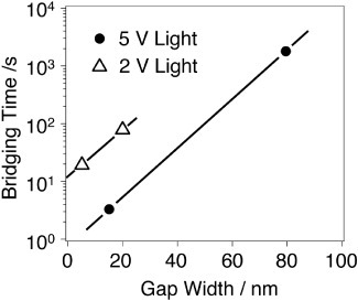
Operation of the photo-assisted atomic switch has been demonstrated using Ag2S as the mixed ionic- and electronic-conductor and N,N’-diheptylperylenetetracarboxylicdiimide (PTCDI) as the photoconductive molecule [Citation54]. The reported switching time for the first demonstration was very long (about 1000 s) because of the large gap size (80 nm) between the two electrodes. However, the switching time was drastically shortened by decreasing the gap size, as shown in figure . Comparison between the plots for applied bias voltages of 5 and 2 V suggests that increasing the bias can also reduce the bridging time. Moreover, much faster switching can also be expected from gap-type atomic switches [Citation25, Citation29]. The switching voltage, retention time and on/off ratio are similar to those of gap-type atomic switches. Cyclic endurance is an issue that needs to be investigated, because a metal filament grows into the photoconductive molecular layer and can damage it.
Figure 16 Plot of bridging time versus gap width. Black dots and white triangles correspond to biases of 5 and 2 V, respectively. (Reproduced with permission from [Citation54] ©2010 Wiley-VCH Verlag GmbH & Co.)
Learning abilities of atomic switches
Neural computing requires learning abilities, which have been imitated by CMOS circuits with analog devices and by software programming [Citation55]. The development of devices having inherent learning abilities will enable the realization of all-hardware neural computing systems.
Learning abilities, such as short-term (ST) and long-term (LT) memories and neuroplasticity, have been demonstrated using Ag2S-based atomic switches [Citation53]. In our brain, information is first stored in the ST memory and then, through repetition of stimuli, is shifted to the LT memory. Although information stored in the ST memory is easily erased, once moved to the LT memory it becomes stable and requires strong and/or multiple unlearning processes for it to be erased. Both ST and LT memories have been realized in a single nanoionic device [Citation53].
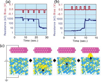
Neuroplasticity refers to changes that occur in the organization of the brain as a result of experience. Namely, a certain number of input signals are required to make a connection in a neural network. The storage of information without any change in the output is required for neuroplasticity; this cannot be achieved with the memory effect or a multistate memory. Neuroplastic behavior has been demonstrated in atomic switches made of small Ag2S grains. Figure (a) shows the experimental trace for turning on an atomic switch with small Ag2S grains using −60 mV, 0.5 s pulses. The resistance of the atomic switch remained constant for the first three input signals but sharply dropped from 1 MΩ to 10 kΩ in the fourth input signal. This result means that the atomic switch with small Ag2S grains stored the information during the first three input steps and ‘fired’ (was turned on) at the fourth input signal. Figure (b) shows the turn-off process, where the resistance of the atomic switch showed no change during the first two input steps but exhibited a small increase in the third input step and a large increase in the fourth step. Therefore, multiple input pulses are required to turn an atomic switch with small Ag2S grains on and off.
Figure 17 (a) Experimental trace for turning on a switch with −60 mV, 0.5 s pulses. (b) Turning off the switch with 60 mV, 0.5 s pulses. (c) Schematic model of the learning mechanism. A series of input signals is required for switching through making the Ag cations cross the grain boundaries. (Reproduced with permission from [Citation53] ©2010 Wiley-VCH Verlag GmbH & Co.)
Applications of atomic switches
Memories
Atomic switches are nonvolatile bipolar switches and require bipolar bias voltages for writing and erasing. Thus, new designs for cell structures, peripheral circuits and architectures are needed for atomic switches to become commercially viable. However, atomic switches have the potential to extend the technology below the 11 nm node, which is sufficient reason for the development of new designs. For instance, switching phenomena have been observed using an ionic conductive nanowire of 20 nm diameter [Citation15]. Atomic force microscopy observation of a conductive area on the surface of an ionic conductive material has suggested that the diameter of the conductive path is at the nanometer scale [Citation56, Citation57].
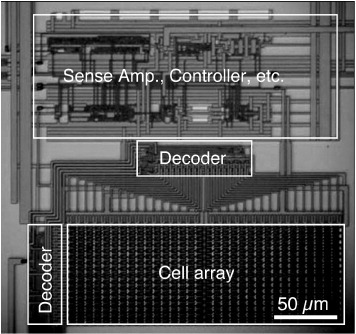
A 1 kB nonvolatile memory chip has been developed using gapless Cu2S atomic switches [Citation58], as shown in figure . The peripheral circuits for reading and writing atomic switches have also been developed on the basis of 1T–1S technology, which uses one transistor (1T) for each atomic switch (1S) to select whether the atomic switch is to be read or written.
Figure 18 A 1 kB nonvolatile memory chip that uses atomic switches. (Reproduced with permission from [Citation58] ©2005 IEEE.)
Logic devices
Two-terminal atomic switches can be used to configure logic circuits such as logic gates [Citation18], as shown in figure . An AND gate consists of two gap-type atomic switches, and input signals (V1 and V2) are applied to Pt electrodes. VOUT measured at one of the ends of a Ag2S wire becomes high (0.5 V) only when a high voltage (0.5 V) is applied to both Pt wires. Thus, it acts as an AND gate, as shown in figure (a). An OR gate is also made of two gap-type atomic switches with two Ag2S wires and a Pt wire, as shown in figure (b). VOUT for this system becomes low only when both of the input signals are low, which is OR gate operation. A NOT gate consists of a single atomic switch with resistors and a capacitor, as shown in figure (c). Here, VOUT becomes low when the input is high, and vice versa. This NOT gate operation is achieved by charging/discharging the current in the capacitor, which turns off/on the atomic switch.
Figure 19 Logic gates configured using atomic switches. (Reproduced with permission from [Citation18] ©2005 NPG.)
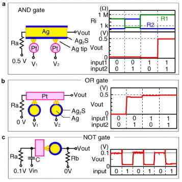
While AND and OR gates can be configured using conventional two-terminal devices, such as rectifiers, resistors and capacitors, NOT gates cannot be formed using them. NOT gates are essential to creating all kinds of logic circuits and three-terminal devices such as semiconductor transistors have been used to construct the NOT gates. The nonvolatility of atomic switches allows the NOT operation to be achieved using only two-terminal devices, as shown in figure (c). Thus, using atomic switches, all three basic logic gates can be constructed with two-terminal devices, meaning that all types of logic circuits can theoretically be designed without resorting to semiconductor transistors.
Crossbar circuits, which have functional two-terminal switches at each crossing point, have been proposed as defect-tolerant logic circuits [Citation59]. The basic operations have been demonstrated using molecular switches [Citation59] and ReRAMs [Citation60]. Both gap-type and gapless-type atomic switches are also useful for configuring crossbar circuits.
In addition, three-terminal atomic switches can also be used in logic circuits [Citation59]. While nonvolatile three-terminal atomic switches are potentially applicable in nonvolatile logic circuits [Citation61], volatile three-terminal atomic switches have an advantage over nonvolatile ones in that they can fully utilize highly integrated CMOS technology [Citation62].
Programmable switches
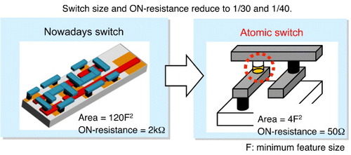
One of the most promising applications of atomic switches is as programmable switches for reconfigurable large-scale integrated circuits (LSIs), such as the field-programmable gate arrays (FPGAs), which can provide various functions by changing the circuits under the control of programmable switching circuits. However, the switching circuit used in conventional FPGAs is composed of a pass transistor combined with either a static random access memory (SRAM) or a flip-flop circuit, which makes the switching circuit as large as 120 F2, where F is the minimum feature size [Citation58]. Consequently, today's FPGAs have a large area reserved for the switching circuits, limiting the device performance. The high on-resistance of the switching circuit (1–2 kΩ) restricts the number of switches on a single chip. Because of these characteristics of present-day switching circuits, FPGAs must use coarse-grained logic cells.
The atomic switch, which is a small nonvolatile device, acts as a switching circuit by itself. Since it can be formed at the crossing point of two wires, the size of the switching circuit is 4F2, 30 times smaller than a conventional switching circuit. The on-resistance of the atomic switch is on the order of 10 Ω, thus reducing the on-resistance of the switching circuit to one-fortieth, as shown in figure . Consequently, a much larger number of switching circuits can be used on a single chip of the FPGA; thus, a large logic cell can be divided into fine logic cells to improve the logical efficiency. Programmable switching was first demonstrated using Cu2S gapless-type atomic switches, which were integrated on the topmost layer of CMOS devices [Citation58], and was recently demonstrated using Ta2O5, thus enabling the integration of atomic switches into the metal layers of CMOS devices [Citation37].
Figure 20 Comparison between semiconductor-transistor-based and atomic-switch-based switching circuits.
Summary
Atomic switches are a new type of nanoionic devices that operate by controlling the formation and annihilation of metal filaments between two electrodes by a solid electrochemical reaction. There are several types of atomic switches including gap-type, gapless-type and three-terminal types. The development of metal-oxide-based atomic switches, which are fully compatible with the CMOS process, has demonstrated the potential for their commercialization. In addition to nonvolatility, new functions of atomic switches, such as memory effects, photosensing and learning abilities, have been developed. The potential for downscaling beyond the 11 nm technology node will also determine the importance of atomic switches as prospective ‘beyond-CMOS’ devices.
References
- MooreG E 1965 Electronics Magazine 19 April. Although he originally predicted the doubling period as every 12 months, he altered it to every 24 months in 1975x
- International Technology Roadmap for Semiconductors, ITRS 2009 edn (www.itrs.net/Links/2009ITRS/Home2009.htms)
- NikonovD EBourianoffG IGarginiP A 2008 J. Nanoelectron. Optoelectron. 3 3 http://dx.doi.org/10.1166/jno.2008.002
- MatsunagaSHayakawaJIkedaSMiuraKHasegawaHEndohTOhnoHHanyuT 2008 Appl. Phys. Express 1 091301 http://dx.doi.org/10.1143/APEX.1.091301
- BaoMKhitunAWuYLeeJ-YWangK LJacobA P 2008 Appl. Phys. Lett. 93 072509 http://dx.doi.org/10.1063/1.2975174
- CowburnR P 2003 Proc. Device Res. Conf. p 111
- van der MolenS JLiaoJKudernacTAgustssonJ SBernardLCalameMvan WeesB JFeringaB LSchonenbergerC 2009 Nano Lett. 9 76 http://dx.doi.org/10.1021/nl802487j
- ZhaoY SFuHPengAMaYXiaoDYaoJ 2008 Adv. Mater. 20 2859 http://dx.doi.org/10.1002/adma.v20:15
- JiangGSongYGuoXZhangDZhuD 2008 Adv. Mater. 20 2888 http://dx.doi.org/10.1002/adma.v20:15
- BallardiniRCeroniPCrediAGandolfiM TMaestriMSemararoMVenturiMBalzaniV 2007 Adv. Funct. Mater. 17 740 http://dx.doi.org/10.1002/(ISSN)1616-3028
- BanerjeeS KRegisterL FTutucEReddyDMacDonaldA H 2009 IEEE Electron Device Lett. 30 158 http://dx.doi.org/10.1109/LED.2008.2009362
- WaserRAonoM 2007 Nat. Mater. 6 833 http://dx.doi.org/10.1038/nmat2023
- ArgallF 1968 Solid-State Electron. 11 535 http://dx.doi.org/10.1016/0038-1101(68)90092-0
- GibbonsJ FBeadleW E 1964 Solid-State Electron. 7 785 http://dx.doi.org/10.1016/0038-1101(64)90131-5
- LiangChTerabeKHasegawaTNegishiRTamuraTAonoM 2005 Small 10 971 http://dx.doi.org/10.1002/(ISSN)1613-6829
- SakamotoTListerKBannoNHasegawaTTerabeKAonoM 2007 Appl. Phys. Lett. 91 092110 http://dx.doi.org/10.1063/1.2777170
- TerabeKHasegawaTNakayamaTAonoM 2001 Riken Rev. 37 7
- TerabeKHasegawaTNakayamaTAonoM 2005 Nature 433 47 http://dx.doi.org/10.1038/nature03190
- SakamotoTSunamuraHKawauraHHasegawaTNakayamaTAonoM 2003 Appl. Phys. Lett. 82 3032 http://dx.doi.org/10.1063/1.1572964
- EiglerD MLutzandC PRudgeW E 1991 Nature 352 600 http://dx.doi.org/10.1038/352600a0
- SmithD P E 1995 Science 269 371 http://dx.doi.org/10.1126/science.269.5222.371
- HasegawaTTerabeKSakamotoTAonoM 2009 MRS Bull. 34 929 http://dx.doi.org/10.1557/mrs2009.215
- TerabeKNakayamaTHasegawaTAonoM 2002 J. Appl. Phys. 91 10110 http://dx.doi.org/10.1063/1.1481775
- KudohTFuekiK 1990 Solid State Ionics Tokyo Kodansha/VCH p 47
- TamuraTHasegawaTTerabeKNakayamaTSakamotoTSunamuraHKawauraHHosakaSAonoM 2006 Japan. J. Appl. Phys. 45 L364 http://dx.doi.org/10.1143/JJAP.45.L364
- PascualJ IMendezJGomez-HerreroJBaroA MGarciaNBinhV T 1993 Phys. Rev. Lett. 71 1852 http://dx.doi.org/10.1103/PhysRevLett.71.1852
- OhnishiHKondoYTakayanagiK 1998 Nature 395 780 http://dx.doi.org/10.1038/27399
- TamuraTHasegawaTTerabeKNakayamaTSakamotoTSunamuraHKawauraHHosakaSAonoM 2007 J. Phys.: Conf. Ser. 61 1157 http://dx.doi.org/10.1088/1742-6596/61/1/229
- NayakATamuraTTsuruokaTTerabeKHosakaSHasegawaTAonoM 2010 J. Phys. Chem. Lett. 1 604 http://dx.doi.org/10.1021/jz900375a
- KunduMHasegawaTTerabeKAonoM 2008 J. Appl. Phys. 103 073523 http://dx.doi.org/10.1063/1.2903599
- KunduMTerabeKHasegawaTAonoM 2006 J. Appl. Phys. 99 103501 http://dx.doi.org/10.1063/1.2199067
- Morales-MasisMvan der MolenS JFuW THesselberthM Bvan RuitenbeekJ M 2009 Nanotechnology 20 095710 http://dx.doi.org/10.1088/0957-4484/20/9/095710
- KozickiM NYunMHiltLSinghA 1999 (Pennington, NJ: Electrochemical Society) p 298
- KozickiM NBalakrishnanMGopalanCRatnakumarCMitkovaM 2005 Proc. Non-Volatile Memory Technology Symp. (NVMTS) 2005 p 7
- HaemoriMNagataTChikyowT 2009 Appl. Phys. Express 2 061401 http://dx.doi.org/10.1143/APEX.2.061401
- LiangChTerabeKTsuruokaTOsadaMHasegawaTAonoM 2007 Adv. Funct. Mater. 17 1466 http://dx.doi.org/10.1002/(ISSN)1616-3028
- TadaM et al 2009 IEDM Technical Digest 09-943
- TsuruokaTTerabeKHasegawaTAonoM 2010 Nanotechnology 21 425205 http://dx.doi.org/10.1088/0957-4484/21/42/425205
- BannoNSakamotoTIguchiNSunamuraHTerabeKHasegawaTAonoM 2008 IEEE Trans. Electron Devices 55 3283 http://dx.doi.org/10.1109/TED.2008.2004246
- WaserRDittmannRStaikovGSzotK 2009 Adv. Mater. 21 2632 http://dx.doi.org/10.1002/adma.v21:25/26
- ArataniK et al 2007 Technical Digest—Int. Electron Devices Meeting p 783
- TsunodaK et al 2007 Tech. Dig., IEEE Int. Electron Device Meeting p 767
- KozickiM NParkMMitkovaM 2005 IEEE Trans. Nanotechnol. p 331 http://dx.doi.org/10.1109/TNANO.2005.846936
- BannoNSakamotoTFujiedaSAonoM 2008 Proc. Int. Reliabil. Phys. Symp., Phoenix p 707
- XieF-QNittlerLObermairCSchimmelT 2004 Phys. Rev. Lett. 93 128303 http://dx.doi.org/10.1103/PhysRevLett.93.128303
- XieF-QMaulRObermairCWenzelWSchonGSchimmelT 2010 Adv. Mater. 22 2033 http://dx.doi.org/10.1002/adma.200902953
- BannoNSakamotoTIguchiNKawauraHKaeriyamaSMizunoMTerabeKHasegawaTAonoM 2006 IEICE Trans. Electron. E89-C 1492 http://dx.doi.org/10.1093/ietele/e89-c.11.1492
- SakamotoTIguchiNAonoM 2010 Appl. Phys. Lett. 96 252104 http://dx.doi.org/10.1063/1.3457861
- ChuaL O 1971 IEEE Trans. Circuit Theory CT-18 507 http://dx.doi.org/10.1109/TCT.1971.1083337
- IkedaHTadaK 1980 Sanyo's Couliodes and Memoriodes; Applications of Solid Electrolytes TakahashiTKozawA Cleveland Academic p 40
- StrukovD BSniderG SStewartD RWilliamsR S 2008 Nature 453 80 http://dx.doi.org/10.1038/nature06932
- YangJ JPickettM DLiXOhlbergD A AStewartD RWilliamsR S 2008 Nat. Nanotechnol. 3 429 http://dx.doi.org/10.1038/nnano.2008.160
- HasegawaTOhnoTTerabeKTsuruokaTNakayamaTGimzewskiJ KAonoM 2010 Adv. Mater. 22 1831 http://dx.doi.org/10.1002/adma.v22:16
- HinoTTanakaHHasegawaTAonoMOgawaT 2010 Small 6 1745 http://dx.doi.org/10.1002/smll.201000472
- MeadC 1990 Proc. IEEE 78 1629 http://dx.doi.org/10.1109/5.58356
- LiangChTerabeKHasegawaTAonoM 2007 Nanotechnology 18 485202 http://dx.doi.org/10.1088/0957-4484/18/48/485202
- SzotKSpeierWBihlmayerGWaserR 2006 Nat. Mater. 5 312 http://dx.doi.org/10.1038/nmat1614
- KaeriyamaSSakamotoTSunamuraHMizunoMKawauraHHasegawaTTerabeKNakayamaTAonoM 2005 IEEE J. Solid-State Circuits 40 168 http://dx.doi.org/10.1109/JSSC.2004.837244
- HeathJ RKuekesP JSniderG SWilliamsR S 1998 Science 280 1716 http://dx.doi.org/10.1126/science.280.5370.1716
- XiaQYangJ JWuWLiXWilliamsR S 2010 Nano Lett. 10 2909 http://dx.doi.org/10.1021/nl1017157
- HanyuTAragakiSHiguchiT 1995 IEE Proc. Circuits Devices Syst. 142 165 http://dx.doi.org/10.1049/ip-cds:19951949
- HasegawaT et al 2011 Appl. Phys. Express 4 015204 http://dx.doi.org/10.1143/APEX.4.015204
- SoniRMeuffelsPPetraruAWeidesMKugelerCWaserRKohlstedtH 2010 J. Appl. Phys. 107 024517 http://dx.doi.org/10.1063/1.3291132
- TsunodaKFukuzumiYJamesonJ RWangZGriffinP BNishiY 2007 Appl. Phys. Lett. 90 113501 http://dx.doi.org/10.1063/1.2712777
- YanX BLiKYinJXiaY DGuoH XChenLLiuZ G 2010 Electrochem. Solid-State Lett. 13 H87 http://dx.doi.org/10.1149/1.3279689
- RahamanS ZMaikapSChiuH CLinC-HWuT-YChenY-STzengP-JChenFKaoM-JTsaiM-J 2010 Electrochem. Solid-State Lett. 13 H159 http://dx.doi.org/10.1149/1.3339449
- LiY TLongS BZhangM HLiuQShaoLZhangSWangYZuoQLiuSLiuM 2010 IEEE Electron Device Lett. 31 117 http://dx.doi.org/10.1109/LED.2009.2036276
- ChaDLeeSJungJAnIKimD-W 2010 J. Korean Phys. Soc. 56 846 http://dx.doi.org/10.3938/jkps.56.846
- KozickiM NGopalanCBalakrishnanMMitkovaM 2006 IEEE Trans. Nanotechnol. 5 535 http://dx.doi.org/10.1109/TNANO.2006.880407
- YangY CPanFZengF 2010 New J. Phys. 12 023008 http://dx.doi.org/10.1088/1367-2630/12/2/023008
- PandianRKooiB JOosthoekJ L Mvan den DoolPPalasantzasGPauzaA 2009 Appl. Phys. Lett. 95 252109 http://dx.doi.org/10.1063/1.3276272
- TangLZhouPChenY RChenL YLvH BTangT ALinY Y 2008 J. Korean Phys. Soc. 53 2283 http://dx.doi.org/10.3938/jkps.53.2283
- AhnJ-KParkK-WHurS-GSeongN-JKimC-SLeeJ-YYoonS-G 2010 J. Mater. Chem. 20 1751 http://dx.doi.org/10.1039/b922398c
- TsujiYSakamotoTBannoNHadaHAonoM 2010 Appl. Phys. Lett. 96 023504 http://dx.doi.org/10.1063/1.3285177
- LiuMAbidZWangWHeXLiuQGuanW 2009 Appl. Phys. Lett. 94 233106 http://dx.doi.org/10.1063/1.3151822
- ChenS-SYangC-PXuL-FYangF-JWangH-BWangHXiongL-BYuYMedvedevaI VBärnerK 2010 Solid State Commun. 150 240 http://dx.doi.org/10.1016/j.ssc.2009.11.021
- HekmatshoarM HMirzayiMMirzayiM 2010 Ionics 16 185 http://dx.doi.org/10.1007/s11581-009-0348-y