Abstract
The ferroelectric domain structure of a PbTiO3 thin film on (100) SrTiO3 has been investigated by transmission electron microscopy (TEM). Two types of a-domain were found: one extended through the film to the surface and another comprised small a-domains confined within the film. Dark-field TEM (DFTEM) observation revealed that 180° domains formed near the substrate and stopped their growth 100 nm away from the substrate. The DFTEM observation also revealed that 90° domain boundaries had head-to-tail structures. To confirm the polarization direction obtained by experiments, diffracted intensities under a two-beam condition were simulated using the extended Darwin–Howie–Whelan equations. On the basis of the obtained results, a ferroelectric domain structure model of PbTiO3 thin films on SrTiO3 is proposed.
Introduction
In recent years, ferroelectric films have been extensively investigated for various applications including those in nonvolatile ferroelectric random access memories (FeRAMs), sensors and actuators in micro-electro-mechanical systems [Citation1–3]. The ferroelectric and piezoelectric properties of these films are affected by the domain structure. Therefore, control of the domain structure of ferroelectric films is important.
PbTiO3 (PTO) is a representative ferroelectric material, which also forms solid solutions such as Pb(Zr,Ti)O3 (PZT). PTO has a very large spontaneous polarization [Citation4–6] and a high ferroelectric phase transition temperature Tc=490 °C [Citation4, Citation5]. The domain structure of PTO films has been studied by x-ray diffraction (XRD) analysis, transmission electron microscopy (TEM) and piezoresponse force microscopy (PFM) [Citation7–11]. The domain structure of PTO films depends on the film thickness and the type of fabrication method. Very thin films show the epitaxial relationship PTO〈100〉 ∥SrTiO3 (STO) 〈100〉 [Citation12, Citation13] and contain 180° domains [Citation14–16] whose formation reduces the depolarizing field. When the film thickness reaches a critical value, which varies between 50 and 300 nm depending on the type of fabrication method [Citation7], the films show a characteristic pattern consisting of alternating c-domains aligned to the surface normal and a-domains with the c-axis aligned along either the [100], , [010], or
crystal axis of the STO substrate [Citation12, Citation13]. a-Domains form to relax the strain associated with the phase transition [Citation13]. In films thicker than 1100 nm, c-domains tilt along the fourfold degenerate [110],
,
, and
STO axes [Citation9–11]. The domain structure model of such thick films has been proposed on the basis of XRD and PFM results [Citation9–11].
Despite the aforementioned studies, details of ferroelectric domain structure, including the polarity of domain walls and the polarization direction, have not been reported yet. In particular, local domain structures at the interface between the film and the substrate, need to be analyzed. TEM is an efficient technique for nanoscale material characterization. In addition, the failure of Friedel's law in electron diffraction can be used to clarify the polarization direction. Friedel's law can be expressed as Ig=I-g, where Ig and I-g are the intensities of two reflections with reciprocal lattice vectors of g and −g, respectively; this law is valid even in crystals lacking a symmetry center, within the kinematical theory of diffraction. However, this law fails owing to the dynamical effect [Citation17]. Therefore, in ferroelectric crystals, ferroelectric regions with the polarization P appear as bright areas in dark-field images taken by selecting reflections with g·P> 0 under the two-beam condition [Citation18–20]. This technique is applied in this study to analyze the ferroelectric domain structure and polarization vector of PTO films at the nanoscale.
Experimental details
PTO films were grown on (100) STO substrates at 600 °C by pulsed metalorganic chemical vapor deposition (pulsed-MOCVD), as described elsewhere [Citation21, Citation22]. Their ferroelectric domain structure was studied by TEM and their polarization direction was determined using the failure of Friedel's law.
TEM samples were prepared as follows. Two cross-sectional slabs were glued with Gatan G2 epoxy so that the film surfaces faced each other. This glued specimen was sliced using a diamond saw, and one of its side was mechanically polished to a mirror finish. This polished side was glued on the TEM specimen support grid with G2 epoxy and the other side was polished until the sample thickness was reduced to below 50 μm. This polished side was then dimpled with a Gatan dimple grinder and ion-milled with a Fischone low-angle milling and polishing system (model 1010). A similar thinning procedure was applied to the preparation of plan-view specimens. JEOL JEM-2000FX, JEM-3010 and Topcon EM-002B microscopes were used for TEM.
Results
Ferroelectric domain structure of PbTiO3 films on (100) SrTiO3
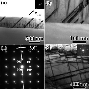
Figures (a)–(d) show bright-field TEM (BFTEM) images and selected area electron diffraction (SAED) patterns of a PTO film on a (100) STO substrate. Two types of a-domain were identified in a cross-sectional image of the film (figure (a)): one grew through the film to the surface and the other stopped its growth within the film. Small a-domains exist within 300 nm from the nearest a-domains. The small a-domains along [101] axis are 50–100 nm in size. The projected domain width of longer a-domains and the distance between them are 30–50 nm and 450–700 nm, respectively. Two adjacent a-domains merged in the magnified image in figure (b). Note that a-domains form a line contact with the substrate. The SAED pattern (figure (c)) taken with an incident beam parallel to the [010] direction reveals that the angle between the surface normal and the [001] axis of c-domains or the [100] axis of a-domains was ∼3.6°, which is larger than that reported previously (2.4°) [Citation9, Citation12, Citation13] because our TEM specimen is very thin and its strain was released during the sample preparation. A plan-view observation (figure (d)) reveals that a-domains intersect at a right angle.
Figure 1 TEM images and diffraction patterns of the PbTiO3 film on SrTiO3: (a) bright-field TEM image when g101 is excited; (b) magnified view showing small a-domains and two merged a-domains; (c) selected area electron diffraction pattern ([010] direction); (d) plan-view image, showing a-domains intersecting at a right angle.
Dark-field TEM (DFTEM) images of the PTO film on the (100) STO substrate were taken to clarify the ferroelectric domain structure. Figures (a) and (b) were obtained using 002 and reflections, respectively, for the [010] electron incidence. SAED patterns were recorded from areas where contrast inversion was observed (marked by circles). A domain with a polarization vector P gives rise to a bright contrast for g·P> 0. Therefore, the contrast in circled areas indicates that 180° domains form near the PTO/STO interface. These 180° domains have a projected width of 10–20 nm, i.e. a period of 20–40 nm. Domain boundaries are perpendicular to the PTO/STO interface and the domain length in the [001] direction is ∼100 nm. The images in figures (a) and (b) were taken from an area more than 100 nm away from the PTO/STO interface using 002 and
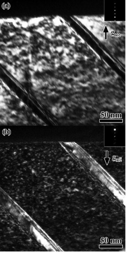
reflections, respectively, for the [010] electron incidence. Contrast inversion was observed in c-domains. This result indicates that the polarization direction in c-domains is parallel to the [001] axis. There is a fine spotty contrast in figures (a) and (b) within c-domains. This contrast showed no inversion upon changing the observation parameters and therefore is likely an artifact introduced during the sample preparation. The polarization direction in a-domains can be determined from DFTEM images taken using 002 and
reflections. However, it is very difficult to set the required diffraction condition for a-domains because of their small size. Hence, the polarization direction of a-domains was determined indirectly by investigating the polarity of 90° domain boundaries.
Figure 2 Cross-sectional DFTEM images and diffraction patterns acquired near the substrate: (a, b) DFTEM images taken using 002 and reflections, respectively. SAED patterns were obtained from the circled regions. The inversion of contrast between the images shows that 180° domains were formed.
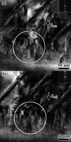
Figure 3 Cross-sectional DFTEM images and diffraction patterns obtained from an area more than 100 nm away from the PbTiO3/SrTiO3 interface: (a, b) DFTEM images taken using 002 and reflections, respectively. Note the contrast inversion between the images.
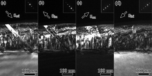
To determine the polarity of 90° domain boundaries, DFTEM images were taken using reflections parallel and perpendicular to the domain boundaries. Figures (a)–(d) were obtained using ,
, 101 and
reflections, respectively, for the [010] electron incidence. A difference in background intensity is observed for diffraction vectors parallel to 90° domain boundaries but not for diffraction vectors perpendicular to 90° domain boundaries. This indicates that 90° domain boundaries have no polarity, i.e. head-to-tail coupling [Citation23].
Figure 4 (a–d) DFTEM images taken using ,
, 101 and
reflections, respectively. The contrast of the 90° domain can be observed in (a) and (b) images, but not in the (c) or (d) image, indicating that 90° domain boundaries have head-to-tail structures.
Simulation of diffracted intensity of PbTiO3
To confirm the polarization direction in ferroelectric domains, the diffracted intensities of PTO were simulated by solving the Darwin–Howie–Whelan equations under a two-beam condition [Citation24, Citation25], extended by Gevers et al [Citation23]. The diffracted intensity, including absorption, is expressed as
where ξ ′0 and ξ ′g are the respective extinction distances of the transmitted and diffracted electron beams, z is the distance from the beam entrance, sg is the excitation error, and θ ′g and θ g are the respective phase angles of the Fourier coefficients of the real and imaginary parts of the electrostatic lattice potential. The parameters required to calculate diffracted intensities were determined from the complex structure factor of PTO calculated by the Weickenmeier–Kohl method [Citation26]. The polarization direction of the unit cell was set parallel to the
direction.
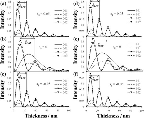
Figures (a)–(c) show the diffracted intensities of the 001, , 002 and
reflections of PTO for sg=+0.05, 0 and −0.05, respectively, and an acceleration voltage of 200 kV. The diffracted intensities and effective extinction distance ξg,eff for sg ≠ 0 were smaller than those for sg=0 (ξg,eff for g=002 or
is shown in figure ). The effective extinction distances for sg ± 0.05 and sg=0 were 16 nm and 27 nm, respectively, when g=002 or
reflection was excited. The diffracted intensity was higher for g=001 than for
, indicating that a domain with a polarization vector P gives rise to a bright contrast for g·P< 0 under a two-beam condition. On the other hand, the diffracted intensity was higher for
than for g=002, indicating that a domain with a polarization vector P produces a bright contrast for g·P > 0. Figures (d)–(f) show the diffracted intensities of 001,
, 002 and
reflections of PTO for sg=+0.05, 0 and −0.05, respectively, and an acceleration voltage of 300 kV. The results are almost the same for 300 kV and 200 kV, with only slightly higher diffracted intensities for 300 kV. In this study, regions with a polarization vector P gave rise to a bright contrast for g·P> 0 under a two-beam condition because 002 and
reflections were used.
Figure 5 Diffracted intensities calculated with the extended Darwin–Howie–Whelan equations: (a, b, c) at 200 kV when the excitation errors are +0.05, 0, and −0.05, and, (d, e, f) at 300 kV when the extinction errors are +0.05, 0, and −0.05, respectively.
Discussion
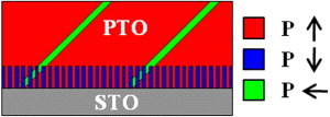
The results of this study reveal that 180° domains were formed near the substrate. The period and length of these 180° domains were 20–40 nm and 100 nm, respectively. Figure shows a summary of the ferroelectric domain structure model of the PTO thin film inferred from the experimental results. 180° domains form near the substrate and stop their growth 100 nm away from it; 90° domains form a line contact with the substrate and 90° domain boundaries have head-to-tail structures.
Figure 6 Ferroelectric domain structure model of PbTiO3 thin film on SrTiO3. 180° domains are formed near the substrate; 90° domain boundaries have head-to-tail structures.
The presence of nanoscale 180° domains is expected to have significant effects on electrical properties [Citation27–29]. The 180° domains near the PTO/STO interface are discussed as follows. The change in the polarization across the interfaces produces an electric field that tends to oppose the polarization [Citation30]. This depolarizing field can be reduced in two ways: through compensation by free charges arriving at the interfaces or by the formation of equal fractions of oppositely polarized (180°) domains. However, the former is unlikely in our case because the substrate is an insulator. Equilibrium 180° domains have been studied by several theoretical treatments, including analytical solutions [Citation27, Citation28, Citation31–36], shell-model calculations [Citation37, Citation38] and Monte Carlo simulations using a first-principles-based effective Hamiltonian [Citation39–42]. Stephenson and Elder showed that the period of 180° domains in PTO films on STO is ∼20 nm when the film thickness is 100 nm [Citation34]. Zhao et al proposed a modified scaling law depending on domain wall width and film thickness [Citation36]. The period of 180° domains calculated using the scaling law was ∼35 nm when the domain wall width and film thickness were 1.2 nm and 100 nm, respectively. In their model, the domain length of 180° domains is equal to the film thickness. Their calculated period of 180° domains agrees with the period of 180° domains obtained in this study (20–40 nm). Note that our films are 400 nm rather than 100 nm thick, and the agreement between the theoretical and experimental results is due to the experimental domain length (100 nm) being equal to the film thickness in the calculation (100 nm). We conclude that the period of 180° domains depends on their length.
Next, we consider how to determine the domain length from published data. In the above discussion, 90° domains are not taken into consideration, but they are formed in PTO films to relax residual strain induced by the phase transition and the difference in thermal expansion coefficient between PTO and STO. Then, the interaction between 90° and 180° domains must be taken into account. As Li et al pointed out, the long-range Coulomb interaction promotes antiparallel dipole alignment and thus 180° domain walls whereas minimization of the gradient energy (interfacial energy) favors 90° domain walls [Citation43]. Meyer and Vanderbilt also pointed out that the energy is about 4 times lower for 90° domain walls than for 180° domain walls [Citation44]. This is one of the factors for stopping the growth of 180° domains because such growth increases interfacial energy. Note that the long-range elastic interaction associated with ferroelectric phase transitions [Citation45] cannot be neglected, and the effects of substrate constraint [Citation46] have to be taken into account for thin films. It is generally presumed that a long-range elastic interaction hinders domain growth. We therefore propose that such an interaction is one of the factors hindering the growth of both 180° and 90° domains (small domains in figures (a) and (b)). However, both interfacial energy (domain wall energy) and elastic interaction can hinder the growth of 180° domains and their contributions are difficult to separate experimentally.
Conclusions
We have investigated the ferroelectric domain structure of PbTiO3 thin films on SrTiO3 by transmission electron microscopy and the major results can be summarized as follows.
PTO thin films on STO show a typical polydomain structure. Cross-sectional BFTEM images show two types of a-domain. One extends through the film to the surface and another stops its growth within the film. a-Domains make a line contact with the substrate. A plan-view observation revealed that a-domains intersect at right angles.
DFTEM revealed ferroelectric domain structures with 180° domains formed near the substrate. These 180° domains stop their growth 100 nm away from the substrate. It was found that 90° domain boundaries show head-to-tail structures.
From these results, we conclude that 180° domains are formed to reduce depolarizing field energy. We also suggested that the length of 180° domains is determined by the competition among the depolarizing field energy, domain wall energy, Coulomb interaction and elastic interaction.
Acknowledgments
This work was supported in part by the Global COE Program ‘Materials Integration International Center of Education and Research, Tohoku University’, financed by MEXT, Japan. TEM observation was carried out at the High-Voltage Electron Microscopy Center of Tohoku University and the Analytical Research Core for Advanced Materials, Institute for Materials Research, Tohoku University. We thank Mr Eiji Aoyagi, Mr Yuichiro Hayasaka and Mr Shun Itoh for assistance with the TEM observation.
References
- PollaD LFrancisL F 1998 Annu. Rev. Mater. Sci. 28 563 http://dx.doi.org/10.1146/annurev.matsci.28.1.563
- SetterNet al 2006 J. Appl. Phys. 100 051606 http://dx.doi.org/10.1063/1.2336999
- MuraltP 2008 J. Am. Ceram. Soc. 91 1385 http://dx.doi.org/10.1111/j.1551-2916.2008.02421.x
- ShiraneGHoshinoSSuzukiK 1950 Phys. Rev. 80 1105 http://dx.doi.org/10.1103/PhysRev.80.1105
- SmolenskiiG A 1951 J. Sov. Tech. Phys. 21 1045
- ShiraneGPepinskyRFrazerB C 1956 Acta Crystallogr. 9 131 http://dx.doi.org/10.1107/S0365110X56000309
- LeeKBaikS 2006 Annu. Rev. Mater. Res. 36 81 http://dx.doi.org/10.1146/annurev.matsci.36.090804.094613
- StemmerSStreifferS KErnstFRühleMHsuW YRajR 1995 Solid State Ionics 75 43 http://dx.doi.org/10.1016/0167-2738(94)00151-H
- NakakiHKimY KYokoyamaSIkariyamaR, FunakuboHNishidaKSaitoK 2007 Appl. Phys. Lett. 91 112904 http://dx.doi.org/10.1063/1.2779239
- NakakiHKimY KYokoyamaSIkariyamaRFunakuboHStreifferS KNishidaKSaitoKGruvermanA 2008 J. Appl. Phys. 104 064121 http://dx.doi.org/10.1063/1.2981193
- UtsugiSFujisawaTIkariyamaRYasuiSNakakiHYamadaTIshikawaMMatsushimaMMoriokaHFunakuboH 2009 Appl. Phys. Lett. 94 052906 http://dx.doi.org/10.1063/1.3078400
- KwakB SErbilABudaiJ DChishlomM FBoatnerL AWilkensB J 1994 Phys. Rev. B 49 14865 http://dx.doi.org/10.1103/PhysRevB.49.14865
- HsuW YRajR 1995 Appl. Phys. Lett. 67 792 http://dx.doi.org/10.1063/1.115469
- StreifferS KEastmanJ AFongD DThompsonCMunkholmAMurtyM V RAucielloOBaiG RStephensonG B 2002 Phys. Rev. Lett. 89 067601 http://dx.doi.org/10.1103/PhysRevLett.89.067601
- FongD DStephensonG BStreifferS KEastmanJ AAucielloOFuossP HThompsonC 2004 Science 304 1650 http://dx.doi.org/10.1126/science.1098252
- ThompsonCFongD DWangR VJiangFStreifferS KLatifiKEastmanJ AFuossP HStephensonG B 2008 Appl. Phys. Lett. 93 182901 http://dx.doi.org/10.1063/1.3013512
- FujimotoF 1959 J. Phys. Soc. Japan 14 1558 http://dx.doi.org/10.1143/JPSJ.14.1558
- TanakaMHonjoG 1964 J. Phys. Soc. Japan 19 954 http://dx.doi.org/10.1143/JPSJ.19.954
- AsadaTKoyamaY 2004 Phys. Rev. B 70 104105 http://dx.doi.org/10.1103/PhysRevB.70.104105
- AsadaTKoyamaY 2007 Phys. Rev. B 75 214111 http://dx.doi.org/10.1103/PhysRevB.75.214111
- NagashimaKArataniMFunakuboH 2000 Japan J. Appl. Phys. Part 2 39 L996 http://dx.doi.org/10.1143/JJAP.39.L996
- NagashimaKFunakuboH 2000 Japan J. Appl. Phys. Part 1 39 212 http://dx.doi.org/10.1143/JJAP.39.212
- GeversRBlankHAmelinckxS 1966 Phys. Status Solidi 13 449 http://dx.doi.org/10.1002/(ISSN)1521-3951
- HashimotoHHowieAWhelanM J 1960 Phil. Mag. 5 967 http://dx.doi.org/10.1080/14786436008238315
- HowieAWhelanM J 1962 Proc. R. Soc. A 267 207 http://dx.doi.org/10.1098/rspa.1962.0093
- WeickenmeierAKohlH 1991 Acta Crystallogr. A 47 590 http://dx.doi.org/10.1107/S0108767391004804
- KopalAMokryPFousekJBahnikT 1999 Ferroelectrics 223 127 http://dx.doi.org/10.1080/00150199908260562
- BratkovskyA MLevanyukA P 2000 Phys. Rev. Lett. 84 3177 http://dx.doi.org/10.1103/PhysRevLett.84.3177
- BratkovskyA MLevanyukA P 2001 Phys. Rev. B 63 132103 http://dx.doi.org/10.1103/PhysRevB.63.132103
- StrukovB ALevanyukA P 1998 Ferroelectric Phenomena in Crystals: Physical Foundations Berlin Springer ISBN-13: 978–3540631323, p 129
- MitsuiTFuruichiJ 1953 Phys. Rev. 90 193 http://dx.doi.org/10.1103/PhysRev.90.193
- BjorkstamJ LOettelR E 1967 Phys. Rev. 159 427 http://dx.doi.org/10.1103/PhysRev.159.427
- KopalABahnikTFousekJ 1997 Ferroelectrics 202 267 http://dx.doi.org/10.1080/00150199708213485
- StephensonG BElderK R 2006 J. Appl. Phys. 100 051601 http://dx.doi.org/10.1063/1.2337360
- LiuGWangR HSunJ 2007 Scr. Mater. 56 337 http://dx.doi.org/10.1016/j.scriptamat.2006.11.009
- ZhaoG PChenLWangJ 2009 J. Appl. Phys. 105 061601 http://dx.doi.org/10.1063/1.3055355
- TinteSStachiottiM G 2001 Phys. Rev. B 64 235403 http://dx.doi.org/10.1103/PhysRevB.64.235403
- StachiottiM G 2004 Appl. Phys. Lett. 84 251 http://dx.doi.org/10.1063/1.1637142
- WuZHuangNLiuZWuJDuanWGuB LZhangX W 2004 Phys. Rev. B 70 104108 http://dx.doi.org/10.1103/PhysRevB.70.104108
- NaumovI IBellaicheLFuH 2004 Nature 432 737 http://dx.doi.org/10.1038/nature03107
- KornevIFuHBellaicheL 2004 Phys. Rev. Lett. 93 196104 http://dx.doi.org/10.1103/PhysRevLett.93.196104
- WuZHuangNWuJDuanWGuB L 2005 Appl. Phys. Lett. 86 202903 http://dx.doi.org/10.1063/1.1929868
- LiB LLiuX PFangFZhuJ LLiuJ M 2006 Phys. Rev. B 73 014107 http://dx.doi.org/10.1103/PhysRevB.73.014107
- MeyerBVanderbiltD 2002 Phys. Rev. B 65 104111 http://dx.doi.org/10.1103/PhysRevB.65.104111
- HuH LChenL Q 1997 Mater. Sci. Eng. A 238 182 http://dx.doi.org/10.1016/S0921-5093(97)00453-X
- LiY LHuS YLiuZ KChenL Q 2002 Acta Mater. 50 395 http://dx.doi.org/10.1016/S1359-6454(01)00360-3