Abstract
Graphene-based nano-objects such as nanotrenches, nanowires, nanobelts and nanoscale superstructures have been grown by surface segregation and precipitation on carbon-doped mono- and polycrystalline nickel substrates in ultrahigh vacuum. The dominant morphologies of the nano-objects were nanowire and nanosheet. Nucleation of graphene sheets occurred at surface defects such as step edges and resulted in the directional growth of nanowires. Surface analysis by scanning tunneling microscopy (STM) has clarified the structure and functionality of the novel nano-objects at atomic resolution. Nanobelts were detected consisting of bilayer graphene sheets with a nanoscale width and a length of several microns. Moiré patterns and one-dimensional reconstruction were observed on multilayer graphite terraces. As a useful functionality, application to repairable high-resolution STM probes is demonstrated.
Introduction
Nanotechnology-driven materials research plays a key role both in basic science and industrial innovations such as next-generation electronic devices. As a promising class of innovative nanomaterials, graphene and graphene-based nano-objects have attracted much interest in both academia and industry because of their unique electronic, mechanical and optical properties [Citation1–5]. These properties stem from such structural characteristics as nanosize, low dimensionality, interatomic-layer coupling, atomic defects, among others [Citation6, Citation7]. Graphene and related nanomaterials such as carbon nanotubes (CNTs) can be produced by mechanical exfoliation [Citation1], chemical vapor deposition (CVD) [Citation8, Citation9], decomposition of SiC [Citation10] and other techniques. Among the various synthesis methods, CVD is promising for industrial applications because of its compatibility with the semiconductor technology. As for the substrates, it should be noted that the Ni(111) surface provides one of the best templates for graphene growth owing to its small mismatch of lattice constant with that of graphene [Citation11].
This article focuses on an unconventional synthesis method of graphene and related materials using internal carbon source and thermal treatment in vacuum [Citation12, Citation13]. Surface enrichment of dopants on various metal surfaces, especially of nickel and its alloys, with dissolved carbon atoms has been studied in ultrahigh vacuum (UHV) from scientific and engineering viewpoints [Citation14–17]. Two-dimensional (2D) enrichment of the topmost surface with solute elements is called ‘surface segregation’, which is defined as the solute accumulation of less than monolayer coverage (θ < 1) at the surface. 3D enrichment is called ‘surface precipitation’, which is defined as 3D nucleation and growth of solute phases. Therefore, the coverage of the precipitated layer is larger than unity (θ > 1). Surface precipitation of carbon on carbon-doped Ni(111) surfaces has attracted particular interest because of its unique properties such as epitaxial graphene growth, existence of stable graphene phase and 2D phase transitions [Citation14, Citation15]. The epitaxial growth of graphene on Ni(111) surfaces is facilitated by the small mismatch of the lattice constants: the hexagonal lattice constant of Ni(111) plane varies between 0.249 and 0.252 nm in the temperature range 573–1173 K [Citation18]. By comparison, the hexagonal lattice constant of graphite basal plane is 0.246 nm in the corresponding temperature range [Citation19]. Furthermore, the growth of graphene-based carbon nanowires was discovered on the graphite(0001) ultrathin films, which were formed by surface precipitation on the carbon-doped Ni(111) substrate [Citation20, Citation21]. This discovery shows that the synthesis of graphene layers by surface segregation and precipitation is accompanied by the creation of graphene-based nanostructures as by-products. One of the motivations of this study is to explore such new structures.
In this paper, we present nanoscale synthesis of graphene-based nanostructures via surface segregation and precipitation on C-doped Ni substrates, as well as their characterization by scanning tunneling microscopy (STM), low-energy electron diffraction (LEED) and Auger electron spectroscopy (AES). Not only monocrystalline Ni(111) surfaces but also polycrystalline Ni plates and wires have been used as the substrates aiming at industrial applications. Novel graphene-based nanostructures have been discovered and characterized and their chemical inertness was applied to the production of robust STM tips.
Experimental details
Monocrystalline Ni(111) plates (99.995% purity, 0.5 mm thickness), polycrystalline Ni plates (99.9% purity, 0.1 mm thickness) and Ni wires (99.995% purity, 0.1 mm diameter) were used as base materials. Doping of carbon was performed by solid-phase diffusion of high-purity carbon (graphite 99.998%) into Ni in high vacuum (∼10−6 Pa) at elevated temperatures for about 14 days in order to reach the thermal equilibrium. The carbon concentration of the Ni substrates was varied from 0.3 to 1.0 at.% by controlling the doping temperature between 1010 and 1290 K, and all carbon concentrations in this paper are given in at.%. The carbon doping level was estimated from the solubility of carbon in nickel [Citation22]. The plate specimens were mirror polished with alumina powder (diameter 0.05–1.0 μm). After ultrasonic degreasing in acetone they were placed in a UHV system (∼10−8 Pa) equipped with LEED, AES, STM and other surface analysis tools. There the samples were heated for several hours to clean their surfaces and gradually cooled down to room temperature. During the cooling, surface segregation and precipitation occurred, and graphene-related nanostructures were produced. Then the samples were characterized by LEED, AES, STM and scanning tunneling spectroscopy (STS) without exposing to air. Electropolished tungsten tips cleaned by 1 keV Ar+ ion sputtering or freshly cut Pt–Ir tips were used for the STM observations.
The C-doped polycrystalline Ni wires were cut and used as STM tips. After the heat treatment in UHV, their surfaces were covered by graphene nanostructures, which were analyzed by field-emission scanning Auger microscopy. To clarify their performance as high-resolution and inert STM probes, atomically clean Si(111)-(7×7) surfaces (n-type, P-doped, 0.01 Ω cm) were measured before and after exposure to the air.
Results and discussion
Graphene-based nano-objects
The C-doped Ni(111) surfaces were first checked by LEED and AES after the carbon enrichment process. A typical LEED pattern and an AES spectrum are shown in figures (a) and (b), respectively. The LEED pattern has a sixfold symmetry, which is consistent with the reciprocal unit cell of the graphite(0001) surface. The AES spectrum shows carbon on the Ni(111) surface as expected. The surface carbon concentration was estimated from the C KLL and Ni LMM peaks as 90%, which corresponds to a multilayer graphene film of a few nanometers in thickness. Thus, the topmost surface is composed of carbon atoms arranged as monocrystalline graphite(0001) with an epitaxial relation to the Ni(111) substrate.
Figure 1 A typical LEED pattern (a) and an Auger electron spectrum of a 0.3% C-doped Ni(111) substrate, which was annealed for surface precipitation. (c) An STM height image of various types of graphene-based nanostructures measured with a tungsten tip at room temperature in UHV (Vs=1.5 V, It=58 pA). Symbols in (c) mean rt: rough terrace, nt: nanotrench, mw: Moiré pattern, nw: nanowire and rc: reconstruction.
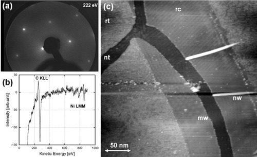
In the case of Ni(111) substrates doped with 0.3% carbon, interesting STM topography images involving various graphene-based nano-objects were obtained at room temperature as shown in figure (c). The sample was annealed at 1150 K for 1 h followed by cooling at 2.2 K min−1 in UHV. Its surface is composed of graphite(0001) terraces and various nanostructures. A long narrow ditch (‘nanotrench’) has been formed in the central area, and two wire-like objects are seen at its edge. The shape and growth of such nanowires resemble those of bean sprouts and therefore these nanowires are called ‘carbon nanosprouts’ [Citation20, Citation21]. A relatively rough area and a smooth area can be distinguished on the topmost terrace. The rough area is composed of surplus carbon atoms, which would be used for the construction of an additional graphene layer. Two periodic patterns are observed on the smooth area: surface reconstruction with 1D periodicity and a Moiré pattern with a 2D periodicity and a sixfold symmetry.
Nanotrench, nanowire and reconstruction
Figures (a) and (b) show a magnified STM topography image and a line profile across the nanotrench formed on the precipitated graphite(0001) thin film, respectively. The 1D reconstruction pattern is recognized both on the right-side upper terrace and on the lowered terrace in the nanotrench. A 2D periodic pattern or a Moiré pattern is seen on the left-side upper terrace. The cross-sectional profile along the white line in the STM image (a) indicates that the depth of the nanotrench is about 330 pm, which agrees with the interlayer distance (335 pm) of graphite(0001). Thus, the graphene-based nanotrench can be defined as a nanoscale ditch formed on multilayer graphene with a monolayer depth. The mechanism of the nanotrench formation is still unclear. Since the step profiles of the confronting sides of the nanotrench are complementary, it may be speculated that the nanotrench is created by tearing of the topmost graphene layer. Rupturing the topmost graphene layer requires significant tensile stress. Even if such stress could exist in the sample, it would be difficult to explain breaking of only the top layer. An alternative explanation could be that the nanotrenches results from the etching of graphene grain boundaries during the annealing. In situ atomic-resolution imaging of the sides of such nanotrenches by high-temperature STM should clarify this issue.
Figure 2 (a) An STM height image of a nanotrench formed in a graphite(0001) terrace on a 0.3% C-doped Ni(111) substrate, measured with a tungsten tip at room temperature in UHV (Vs=1.5 V, It=69 pA). (b) A cross-sectional profile along the white line in panel (a). The depth of the nanotrench (∼330 pm) corresponds to a monolayer height of graphite(0001) terrace.
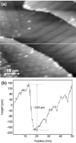
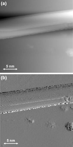
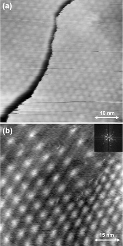
Figure revealed growth of nanowires from the step-edges of the nanotrench. Magnified STM topography and tunneling current images of a nanowire grown on the graphite(0001) terrace are shown in figures (a) and (b), respectively. This nanowire is about ∼2 nm tall, ∼5 nm wide and ∼100 nm long; however, note that the STM topography image is always dilated by the shape of the tip apex with a finite curvature radius [Citation23, Citation24]. The STM current image (b) shows the atomically resolved structure of the nanowire more clearly and indicates the similarity with that of a CNT [Citation25]. Thus, the observed nanowire is made of rolled-up graphene sheets. At first glance, the nanowire looks like a single nanowire as shown in figure (c). However, the atomically resolved STM images in figure suggest that the nanowire consists of two or three graphene sheets with different rolling orientations. The observed complex nanostructure can be attributed to ripples formed on the graphene sheet or to a bundle of a few narrower nanowires.
Figure 3 Height (a) and current (b) STM images of a carbon nanowire grown on a graphite(0001) terrace on a 0.3% C-doped Ni(111) substrate, measured with a tungsten tip in UHV (Vs=−1.52 V, It=0.95 nA).
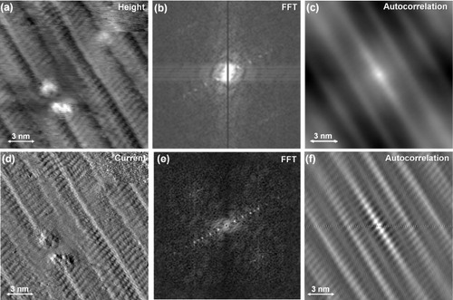
Figures (a)–(f) show atomically resolved STM topography and tunnel-current images of 1D reconstruction pattern formed on the graphite(0001) terrace, the corresponding 2D fast Fourier transform (FFT) images, and the autocorrelation images, respectively. The topmost graphene layer is corrugated along one of the threefold symmetry directions. Both FFT images show equally spaced dots along the specified direction and faint diffraction spots of a 2D atomic lattice, from which the periodicity of the 1D reconstruction was estimated. The autocorrelation images of figures (c) and (f) clearly reveal the one-dimensionality of the reconstruction at the atomic scale. The observed interval and corrugation of the 1D reconstruction are ∼3 nm and ∼50 pm, respectively. Superstructures have been previously observed by STM on a graphite(0001) surface near defects such as atomic vacancies, steps, holes or adsorbed metal particles [Citation26, Citation27]. These superstructures had a threefold symmetry and a periodicity of (√3×√3)a where a=0.246 nm. However, we are unaware of reports on such a 1D surface reconstruction as we have observed on the graphite(0001) surface. The 1D reconstruction on the topmost graphite(0001) planes may be related to the release of stress and strain. A similar 1D reconstruction caused by surface stress on the Au(111) surface is called herringbone reconstruction. There the 23×√3 reconstruction is induced by the spontaneous formation of a stress domain [Citation28]. We hope to present a detailed analysis of the observed 1D reconstruction based on low-temperature STM/STS measurements with higher spatial resolution in the near future.
Figure 4 STM images of a 1D reconstruction pattern formed on a graphite(0001) terrace on a 0.3% C-doped Ni(111) substrate, measured with a tungsten tip (Vs=−1.5 V, It=1.1 nA). (a) An STM height image and (d) an STM current image; (b) and (e) are the FFT images of (a) and (d), respectively; (c) and (f) are the autocorrelation images of (a) and (d), respectively.
Moiré patterns
Giant superstructures with hexagonal symmetry on graphite(0001) and graphene have been observed by atomically resolved STM and noncontact atomic force microscopy [Citation29, Citation30]. These superstructures are Moiré patterns caused by rotational misorientation of the topmost graphene layer relative to the underlying graphite(0001) substrate. Figures (a) and (c) respectively show STM height and current images of a typical Moiré pattern on a graphite(0001) thin film on a 0.4% C-doped Ni(111) substrate. The sample was annealed at 1300 K for 40 min and then at 1060 K for 20 min followed by cooling at a rate of 1.4 K min−1 in UHV. Both STM images clearly show periodic patterns with a hexagonal symmetry. Figure (b) is the FFT image of figure (a) indicating a clear hexagonal lattice in the reciprocal space.
Figure 5 (a) An STM height image of Moiré pattern formed on a graphite(0001) terrace on a 0.4% C-doped Ni(111) substrate after annealing for surface precipitation, measured with a Pt–Ir tip (Vs=0.5 V, It=0.3 nA). Panel (b) is the FFT image of (a) and (c) is a simultaneously observed STM current image.
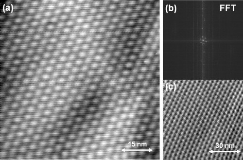
Figure (a) is a unique STM height image hinting the formation mechanism of the Moiré patterns. It suggests that adjacent Moiré patterns were created by the formation of a nanotrench, which tore the topmost graphene layer apart. Such process might induce a rotational misorientation of the topmost layers relative to the graphite(0001) substrate. Another interesting Moiré pattern is shown in figure (b), where the periodicity is not uniform but is gradually changing. The corresponding FFT image shows an elongated spotty pattern with a sixfold symmetry, indicating a linear periodicity change of the Moiré pattern. Uniform Moiré patterns were reported on cleaved graphite(0001) surfaces. In the case of graphite(0001) thin film formed by surface precipitation, intrinsic stress and strain may be more accumulated on the topmost layer, resulting in such unusual Moiré patterns.
Figure 6 STM images of peculiar Moiré patterns formed on graphite(0001) terrace on a 0.4% C-doped Ni(111) substrate measured with a Pt–Ir tip. (a) STM image indicating Moiré patterns formed near a nanotrench on a graphite(0001) terrace (Vs=−0.2 V, It=0.5 nA). (b) An STM height image showing a non-uniform Moiré pattern with a varying periodicity, formed on a graphite(0001) terrace (Vs=0.5 V, It=0.5 nA). The insert is an FFT image of (b) indicating a continuously changing periodicity in reciprocal space.
Graphene nanobelts
Thin strips of graphene called graphene nanoribbons or nanobelts have attracted much attention owing to their unique electronic properties and potential applications as integrated circuit interconnects [Citation31, Citation32]. The synthesis of graphene nanobelts by surface precipitation was first realized on a polycrystalline C-doped (0.4%) Ni sheet. The surface precipitation was induced by dc current heating at 1140 K for 30 min followed by a gradual cooling at a rate of 3.5 K min−1 in UHV. The STM height image of figure (a) shows graphene-based nanowires and nanobelts on a flat graphite(0001) terrace. The wavy shape in the upper-left part of a nanowire is not an artifact such as drift or instability, because it does not show up in other sample areas. It is caused by the lateral dragging of the nanowire by the scanning tip revealing weak adhesion of the nanowire to the substrate. Two belt-like structures (nanobelts) are observed in the right and left parts of the image and are characterized by constant width and height at a relatively long length.
Figure 7 (a) An STM height image of graphene-based nanowires (nw) and nanobelts (nb) formed on a polycrystalline 0.4% C-doped Ni sheet, measured with a Pt–Ir tip at room temperature in UHV (Vs=0.79 V, It=0.1 nA). (b) An STM height image of a graphene nanobelt formed on a 0.4% C-doped Ni(111) substrate, measured with a Pt–Ir tip at room temperature in UHV (Vs=−0.96 V, It=0.1 nA).
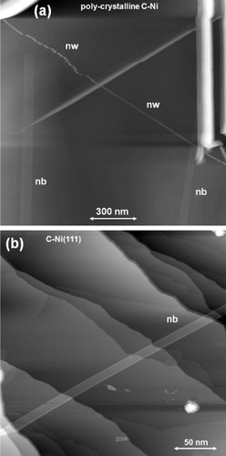
After the discovery of the nanobelts on the polycrystalline C-doped Ni substrate, similar belt-like structures were also observed on the C-doped (0.4%) Ni(111) substrate, as shown in the STM image of figure (b). An interesting and common feature of the nanobelts is protrusions at their both sides. Furthermore, the nanobelts can smoothly follow the underlying steps and terraces of the graphite(0001) surface, indicating their supreme flexibility and elasticity [Citation33].
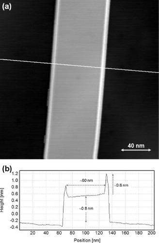
A magnified STM topography image and a cross-sectional profile of the right-side nanobelt in figure (a) are shown in figures (a) and (b), respectively. The height and width of the nanobelts are ∼0.8 nm and ∼60 nm, respectively. This height value is similar to that of bilayer graphene (0.67 nm). The protrusions observed at the both sides of the nanobelts are ∼1.4 nm above the graphite(0001) surface. Atomic-resolution images of the protrusion suggest that the protrusion is composed of the rolled-up graphene and is thus similar to graphene-based nanowires.
Figure 8 (a) An STM height image of a carbon nanobelt formed on a graphite basal plane of a polycrystalline C-doped Ni sheet, measured with a Pt–Ir tip (Vs=0.79 V, It=0.1 nA). (b) Cross-sectional profile along the white line in panel (a). The height of the nanobelt (∼0.8 nm) corresponds to a height of graphene bilayer.
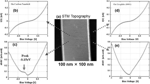
Electronic properties of the nanobelt were characterized by STS as shown in figure . These site-specific STS measurements suggest that the current–voltage characteristics of the nanobelt are apparently similar to those of the graphite(0001) terrace. The I–V curve shows a linear increase of current with increasing voltage around zero bias (Fermi level) indicating semi-metallic conductivity in the nanobelt. The origin of a small peak observed near the Fermi level in the differentiated spectrum is unclear, but it may be attributed to the so-called defect state observed near atomic vacancies [Citation27, Citation34].
Figure 9 Scanning tunneling spectroscopy of a carbon nanobelt measured with a Pt–Ir tip at room temperature. (a) An STM height image (Vs=0.7 V, It=0.1 nA); (b) and (d) current–voltage (I–V) curves of the nanobelt and a graphite terrace; (c) and (e) differentiated (dI/dV) curves of the nanobelt and graphite terrace.
Growth model
Based on the above observations, a schematic growth model of graphene-based nanostructures on a C-doped Ni(111) substrate in vacuum was developed as shown in figure .
Figure 10 Schematic growth model of graphene-based nanostructures on a carbon-doped Ni(111) substrate at elevated temperatures in UHV. At high temperatures, surface carbon atoms are enriched by surface segregation up to a few atomic percent, while the majority of carbon atoms are still dissolved in the bulk. A monolayer graphene phase appears upon cooling where the surface coverage is nearly unity. Further decrease of temperature initiates surface precipitation and the growth of multilayer graphene. Graphene-based structures such as nanowires can grow at defective sites such as steps.
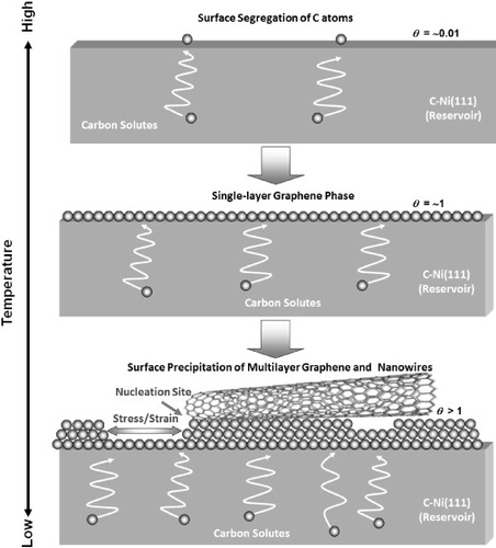
The high-temperature phase is surface segregation of the solute carbon atoms. The coverage of carbon segregates is a few atomic percent (θ=∼0.01), while most of carbon atoms are still dissolved in the bulk. Previous x-ray photoelectron spectroscopy (XPS) measurements revealed that the chemical state of the segregated carbon is atomic like and the carbon atoms are sparsely distributed on the surface [Citation15].
A monolayer graphene phase appears upon cooling from the surface segregation stage. This 2D phase corresponds to a surface coverage θ=∼1. Upon further cooling, the system reaches the temperature at which the bulk carbon concentration exceeds carbon solubility. Then multilayers of carbon start to precipitate on the Ni(111) surface that is already covered with monolayer graphene. Since graphite(0001) basal plane is chemically stable, the growth rate on the (0001) terraces is relatively low. Thus, surface defects such as steps, domain boundaries, atomic vacancies and screw dislocations serve as effective nucleation and growth sites for graphene sheets and other graphene-like nanostructures like nanowires and nanobelts. The nucleation and growth sites are located not only on the topmost surface, but also at the internal interfaces between the Ni(111) substrate and the graphene overlayers. Therefore, tensile stress and strain may accumulate as the surface precipitation proceeds that may result in the formation of nanotrenches on the topmost graphene layer. These defects may produce Moiré patterns due to rotational misorientation and offer additional nucleation sites for graphene-based nanostructures. The origin of the observed 1D surface reconstruction may also be attributed to the surface stress and strain.
The proposed model is a variation of layer-plus-island growth, or the so-called Stranski–Krastanov mode, which is consistent with the previous in-situ XPS analysis [Citation35]. It means that the islands of graphene nanostructures grow on the pre-existing graphene monolayer on the C-doped Ni(111) surface.
The difference between the Ni(111) and polycrystalline Ni substrates is the growth mode. Only Ni(111) substrates have epitaxial relationship with the graphite overlayers grown by surface segregation and precipitation, where the carbon atoms are preferentially arranged in the graphite structure with the epitaxial relationships
Although the graphene overlayers grown on polycrystalline Ni substrates have no such epitaxial relationship, previous reflection high-energy electron diffraction analysis reveals a c-axis oriented growth where the strong (000n) diffraction spots are aligned normal to the surface [Citation16]. It suggests that the graphite(0001) basal planes preferentially cover the polycrystalline Ni surface. The STM image of the graphite overlayer shown in figure clearly demonstrates that the surface is completely covered by the graphite basal planes.
Application to STM probes
As a potential application, STM probes were coated with graphene-based nanostructures aiming to provide the probes with chemical inertness, anti-oxidation ability, electric conductivity and sharp protrusions. Figures (a) and (b) show scanning electron microscopy images of the surface of a C-doped (1.0%) Ni tip with graphitic carbon overlayers formed by surface precipitation. Many nanowires are observed in the graphite overlayers on the C-doped Ni tip, and some are protruding from the surface as shown in figure (b). Auger electron spectra of the surfaces of the C-doped Ni tip before and after the heat treatment are shown in figure (c). They indicate that the surface is fully covered by precipitated carbon atoms after annealing at 1073 K for 1 h in UHV.
Figure 11 (a) An SEM image of a 1.0% C-doped Ni tip with a graphitic overlayer formed by surface precipitation in UHV. (b) An SEM image of a carbon nanowire protruding from the surface. (c) Auger electron spectra of the surfaces of a C-doped Ni tip before and after annealing for surface precipitation.
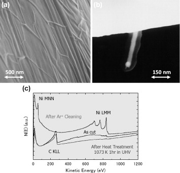
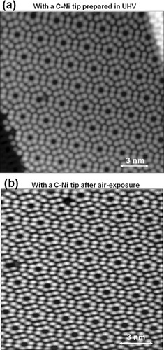
Figure (a) shows an STM height image of an n-type Si(111) surface observed at 80 K in UHV with the C-doped Ni tip with graphitic overlayers. Atomically resolved 7×7 reconstruction and the individual atoms at the step edges are clearly seen indicating a performance similar to that of conventional electropolished tungsten tips. Such tungsten tips are widely used in UHV–STM, but they require in situ cleaning in UHV by electron bombardment or ion sputtering, to remove the oxide layer before the measurement. In order to demonstrate the chemical inertness of the C-doped Ni tip with graphitic overlayers, the tip was exposed to air (T=301 K, relative humidity 59%) for 1 h, and the Si(111) surface was scanned again. Atomically resolved 7×7 reconstruction is clearly observed after exposure in figure (b) indicating the tip stability to chemisorption and oxidation under ambient conditions. Another apparent advantage of the C-doped Ni probe is reparability as the graphitic overlayer can be recovered by annealing in UHV.
Figure 12 (a) An STM height image of an n-type Si(111) surface observed at 80 K with a 1.0% C-doped Ni tip with graphitic overlayers formed by surface precipitation (Vs=1.7 V, It=30 pA). (b) The Si(111) surface observed under the same scanning conditions after exposing the tip to air (T=301 K, humidity=59%) for 1 h.
Conclusions
Graphene-based nanostructures such as nanotrenches, nanowires and nanobelts can be grown on carbon-doped nickel substrates in UHV using surface segregation and precipitation phenomena. Surface analysis with STM clarified the structure and functionality of the novel nano-objects down to the atomic resolution. Their dominant morphologies are nanowire and nanosheet. Nucleation and growth of graphene sheets at surface defects such as step edges may result in the directional growth of nanowires. Graphene-based nanobelts were discovered consisting of bilayer graphene of nanometer width and micrometer length. Superstructures such as Moiré patterns and 1D reconstruction were observed on highly strained graphite terraces. The growth mechanism of the observed nanostructures is based on a bulk-to-surface precipitation of internal carbon atoms. Application of these nanostructures to repairable high-resolution STM probes is demonstrated.
Acknowledgments
The author is grateful to T Kumakura and M Kitahara for their technical assistance. This work was in part supported by the World Premier International Research Center (WPI) Initiative on Materials Nanoarchitectonics, MEXT, Japan.
References
- GeimA KNovoselovK S 2007 Nat. Mater. 6 183 http://dx.doi.org/10.1038/nmat1849
- XiaFMuellerTLinY MValdes-GarciaY AAvourisPh 2009 Nat. Nanotechnol. 476 839 http://dx.doi.org/10.1038/nnano.2009.292
- WuXHuYRuanMMadiomananaN KHankinsonJSprinkleMBergerCde HeerW A 2009 Appl. Phys. Lett. 95 223108 http://dx.doi.org/10.1063/1.3266524
- MintmireJ WDunlapB IWhiteC T 1992 Phys. Rev. Lett. 68 631 http://dx.doi.org/10.1103/PhysRevLett.68.631
- DekkerC 1999 Phys. Today 52 22 http://dx.doi.org/10.1063/1.882658
- PartoensBPeetersF M 2006 Phys. Rev. B 74 075404 http://dx.doi.org/10.1103/PhysRevB.74.075404
- LahiriJLinYBozkurtPOleynikIIBatzillM 2010 Nat. Nanotechnol. 5 326 http://dx.doi.org/10.1038/nnano.2010.53
- ReinaAJiaX THoJNezichDSonHBulovicVDresselhausM SKongJ 2009 Nano Lett. 9 30 http://dx.doi.org/10.1021/nl801827v
- DaiHRintzlerA GNikolaevPThessAColbertD TSmalleyR E 1996 Chem. Phys. Lett. 260 471 http://dx.doi.org/10.1016/0009-2614(96)00862-7
- EmtsevK V et al 2009 Nat. Mater. 8 203 http://dx.doi.org/10.1038/nmat2382
- GamoYNagashimaAWakabayashiMTeraiMOshimaC 1997 Surf. Sci. 374 61 http://dx.doi.org/10.1016/S0039-6028(96)00785-6
- GaoJ HFujitaDXuM SOnishiKMiyamotoS 2010 ACS Nano 4 1026 http://dx.doi.org/10.1021/nn901255u
- XuMFujitaDSagisakaKWatanabeEHanagataN 2011 ACS Nano 5 1522 http://dx.doi.org/10.1021/nn103428k
- SheltonJ CPatilH RBlakelyJ M 1974 Surf. Sci. 43 493 http://dx.doi.org/10.1016/0039-6028(74)90272-6
- FujitaDYoshiharaK 1994 J. Vac. Sci. Techno1. A 12 2134 http://dx.doi.org/10.1116/1.579150
- FujitaDHommaT 1992 Surf. Interface Anal. 19 430 http://dx.doi.org/10.1002/(ISSN)1096-9918
- YamazakiSTanakaMTanakaSFujinamiMUemoriRFujitaDHommaTOnoM 1991 J. Vac. Sci. Technol. B 9 883 http://dx.doi.org/10.1116/1.585488
- WiseE M 1961 Metal Handbook vol 1 8th edn USA American Society for Metals p 1271
- MorganW C 1972 Carbon 10 73 http://dx.doi.org/10.1016/0008-6223(72)90011-5
- FujitaDOhgiTOnishiKKumakuraTHaradaM 2003 Japan. J. Appl. Phys. 42 1391 http://dx.doi.org/10.1143/JJAP.42.1391
- FujitaDKumakuraTOnishiKSagisakaKOhgiTHaradaM 2004 Surf. Sci. 566–568 361 http://dx.doi.org/10.1016/j.susc.2004.05.073
- DunnW WMcLellanR BOatesW A 1968 Trans. AIME 242 129
- GuoXLFujitaD 2007 Japan. J. Appl. Phys. 46 5568 http://dx.doi.org/10.1143/JJAP.46.5568
- XuM SFujitaDOnishiK 2009 Rev. Sci. Instrum. 80 043703 http://dx.doi.org/10.1063/1.3115182
- VenemaL CWildöerJ W GDekkerCRinzlerG ASmalleyR E 1997 Appl. Phys. A 66 S153 http://dx.doi.org/10.1007/s003390051120
- Valenzuela-BenavidesJMorales de laGarzaL 1995 Surf. Sci. 330 227 http://dx.doi.org/10.1016/0039-6028(95)00240-5
- NiimiYNatsuiTKambaraHFukuyamaH 2006 Physica E 34 100 http://dx.doi.org/10.1016/j.physe.2006.02.037
- NarasimhanSVanderbiltD 1992 Phys. Rev. Lett. 69 1564 http://dx.doi.org/10.1103/PhysRevLett.69.1564
- XhieJSattlerKGeMVenkateswaranN 1993 Phys. Rev. B 47 15835 http://dx.doi.org/10.1103/PhysRevB.47.15835
- SunZHämäläinenS KSainioJLahtinenJVanmaekelberghDLiljerothP 2011 Phys. Rev. B 83 081415 http://dx.doi.org/10.1103/PhysRevB.83.081415
- NakadaKFujitaMDresselhausGDresselhausM S 1996 Phys. Rev. B 54 17594 http://dx.doi.org/10.1103/PhysRevB.54.17954
- JiaoLZhangLWangXDiankovGDaiH 2009 Nature 458 877 http://dx.doi.org/10.1038/nature07919
- LeeCWeiXKysarJ WHoneJ 2008 Science 321 385 http://dx.doi.org/10.1126/science.1157996
- FerroYThomasCAngotTGénésioPAlloucheA 2007 J. Nucl. Mater. 363–365 1206 http://dx.doi.org/10.1016/j.jnucmat.2007.01.254
- FujitaDSchlebergerMTougaardS 1995 Surf. Sci. 331–333 348 http://dx.doi.org/10.1016/0039-6028(95)00312-6