Abstract
Thin films are used in a wide variety of computing and communication applications although their fatigue behavior and its dependence on alloying elements are not very well known. In this paper, we present an experimental implementation of a novel high-throughput fatigue testing method for metallic thin films. The methodology uses the fact that the surface strain amplitude of a vibrating cantilever decreases linearly from the fixed end to the free end. Therefore, a thin film attached to a vibrating cantilever will experience a gradient of strain and corresponding stress amplitudes along the cantilever. Each cantilever can be used to extract a lifetime diagram by measuring the fatigue-induced damage front that progresses along the cantilever during up to 108 load cycles.
Introduction
Thin films are key components in microelectronics and micro-electro-mechanical systems (MEMS). While it is common knowledge that, for example, the flow stress in pure thin films differs significantly from that in bulk materials [Citation1, Citation2], there still remain open questions concerning fatigue lifetime and the governing failure mechanisms. Fatigue properties are particularly important in MEMS where the operation frequency and stress amplitude can be lifetime limiting. Therefore, the reliable application of thin films requires the understanding of fatigue mechanisms and the development of fatigue-resistant thin-film alloys.
Fatigue is defined as the failure of a material due to cyclic loading at a level below the ultimate strength [Citation3]. Fatigue properties are usually represented in so-called S–N diagrams where the tolerable stress amplitude (σa) is plotted as a function of the number of cycles to failure Nf [Citation4]. Usually, establishing an S–N diagram is a tedious process because data for each stress level are obtained from a separate specimen; hence, probing the high and very high cycle fatigue regime (HCF and VHCF) is rather time consuming. In this paper, we propose a new high-throughput fatigue testing methodology for thin films based on thin film materials libraries deposited on micro-machined Si cantilever arrays. The motivation for developing this technique is to understand the effect of alloying elements on the fatigue behavior of thin metallic films and to apply this knowledge to the design of fatigue-resistant alloys. We demonstrate the feasibility of this method on the example of Cu thin films.
Fatigue in thin films
In bulk metals, fatigue damage mechanisms have been studied since the 19th century and summarized in textbooks, for example [Citation3]. The damage induced by fatigue testing of metallic bulk materials starts with crack nucleation, followed by stable crack growth and fracture after reaching a critical crack length.
The origin of crack nucleation can be defects in the material or irreversible gliding processes of dislocations on preferred glide planes through the sample, leading to persistent slip bands (PSBs). Dislocation-related processes lead to surface roughening by the formation of extrusions and intrusions from which cracks are nucleated. A microcrack propagates along the plane with the highest Schmid factor until it reorients perpendicular to the highest normal load (mode I crack). From this moment, a stable crack growth takes place. The mechanism of stable crack propagation is plastic flow at the crack tip, which leads to continuous blunting and resharpening of the crack tip profile with every cycle. Macroscopically, this results in fatigue striations on the fracture surface. Once the crack exceeds a critical length, where the stress intensity factor reaches the fracture toughness, unstable crack growth is initiated and the sample fails.
In thin-film applications, at least one dimension of the specimen is less than a few micrometers. This dimensional constraint affects the fatigue behavior [Citation5]. Dislocations in thin films are located closer to the free surface and, therefore, are attracted by image forces. As a result, they can rearrange and escape more easily than those in bulk materials. For the formation of a complex dislocation structure such as PSBs, with a characteristic length scale of about 1 μm, the availability and activation of dislocation sources becomes more limited with decreasing length scale.
This argument has been supported by the observation of fatigue processes in freestanding thin films. Read [Citation6] has found no dislocation structures in freestanding, 1.1 μm thick, damaged Cu samples. In contrast, thin films on substrates have an additional interface to the substrate. This interface, together with the substrate itself, affects the damage formation. The substrate properties have to be differentiated in polymer-based, very compliant substrates and, for example, Si-based, rigid substrates. Polymer-based substrates are of great interest, such as for printable or flexible electronics and may show failure in the low cycle fatigue (LCF) regime with lifetimes of up to 105 cycles [Citation7]. Thin metal films on Si or similarly rigid substrates are ubiquitous in microprocessors, communication devices and MEMS. Such devices typically experience smaller cyclic strain amplitudes, often originating from temperature changes in combination with a thermal mismatch between the metallization and the substrate. The expected lifetime is typically in the high or even very high cycle fatigue (HCF and VHCF) regime. Fatigue damage in the LCF and HCF regimes is sensitive to microstructural parameters like grain size and film thickness [Citation8] with the trend that lifetime increases with decreasing film thickness and grain size. Zhang et al [Citation5] reported that film thickness and grain size have similar effects on the fatigue damage and, since the film thickness limits the grain size in such films, it is difficult to differentiate between these effects. Extensive investigations using transmission electron microscopy (TEM) on Cu thin films revealed that the formation of dislocation structures changes considerably with film thickness and grain size [Citation5]. Thin films of 3 μm thickness still show bulk-like fatigue damage, with clear dislocation structures. In contrast, thinner films with a thickness or grain sizes of less than 500 nm contain only single dislocations [Citation7] and no structures with a long-range order. Further observations indicate that the smallest dimension (either film thickness or grain size) affects the damage mechanism as the size and number of extrusions decrease with decreasing grain size or film thickness [Citation5]. Crack formation also depends on the film thickness: nucleation and (in most cases) propagation of cracks in thick films are controlled by extrusions in a transcrystalline manner, whereas thinner films exhibit intergranular crack propagation. A similar damage formation is observed in Ag thin films on Si substrates [Citation9] and Al thin films subjected to high-frequency loads [Citation10].
Thin films of pure metals are rarely used in technological applications and are often supplanted by alloys. Park et al [Citation11] have investigated the lifetime of Al-3% Ti thin films. They found that these alloyed thin films have a longer fatigue lifetime than bulk Al at the same stress, but are more fatigue sensitive as the lifetime strongly changes for different stress levels. Other examples of fatigue in complex material systems can be found in multilayer systems [Citation12] and the effect of interfaces on fatigue. However, these are specific cases of alloy systems, and there is a lack of systematic knowledge on the effect of alloy composition on the fatigue lifetime and damage mechanisms. To provide a systematic understanding, different alloy systems will be studied using a new combinatorial approach of high-throughput sample fabrication with Si cantilever arrays and fatigue testing.
Cantilever-based high-throughput experiments
Micro-machined Si cantilever arrays are frequently used in combinatorial and high-throughput experimentation and are an important example of MEMS tools [Citation13]. Thin films can be deposited on top of an array of Si cantilevers, and their composition can be varied by using different sputter sources and variable shutters. Such experiments have been carried out to identify and characterize the shape memory [Citation14, Citation15], ferromagnetic shape memory [Citation16, Citation17] and magnetostrictive properties [Citation18] of thin film alloys. Furthermore, material systems for hydrogen storage [Citation19, Citation20] have been studied, and a high-throughput measurement method for ex situ thin film stress measurements [Citation21, Citation22] and chemical sensing [Citation23] was investigated.
Methodology and experimental implementation
Basic idea
First, a thin film is deposited onto the surface of a Si cantilever. Excitation of the cantilever at the resonance frequency of the first bending mode cyclically strains the deposited film with the amplitude equal to the surface strain of the cantilever (see figure ). From beam theory, it is known that the strain varies linearly from the fixed to the free end of the cantilever. Therefore, the strain amplitude at any spot on the surface of the cantilever can be calculated from the maximum deflection of the free end of the cantilever. This is true as long as the film is much thinner than the cantilever and the stiffness of the beam is not affected by the stiffness of the film. The strain is maximum near the fixed end and is zero at the free end of the cantilever (figure (b)). Because of the variation of the strain amplitude, the fatigue lifetime of the film should vary along the cantilever. It is expected that the damaged part of the film will grow with increasing number of cycles, starting from the fixed end of the cantilever.
Figure 1 FE simulation of a Si cantilever (l=12 mm; h=200 μm) excited at its resonance frequency: (a) Comparison of simulation and experimental data at the maximum deflection of the cantilever versus the position along the cantilever. (b) The strain amplitude of the vibrating cantilever decreases linearly along the cantilever with a maximum at the fixed end and zero stress amplitude at the free end. A Young's modulus of 120 GPa for Cu was used to calculate the stress in the thin film.
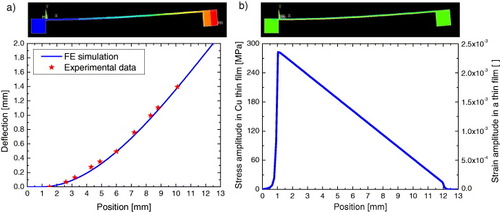
Stress in the film was calculated from its Young's modulus by finite element (FE) simulations (Multiphysics, ANSYS) using a simplified 2D model of the Si cantilever (length 12 mm, thickness 100 μm). The simulations took into account the weight that was attached at the free end of the cantilever to determine its resonance frequency. The model was meshed by 50 μm rectangular elements with eight nodes (Plane82). Figure shows the values of deflection and calculated stress amplitude in a Cu thin film along the position of the cantilever. Within the thin film approximation, we can assume that the strain at the surface of the cantilever is the same as in the attached thin film. As expected, the calculated stress amplitude (figure (b)) in the thin film reaches its maximum at the fixed end, close to the shoulder of the cantilever, and decreases linearly towards the free end. This gradient along the cantilever affects the local lifetime of the thin film, and by detecting the damage front along the cantilever during the fatigue experiment, as shown schematically in figure , an S–N diagram can be acquired. Thus, the fatigue properties of an entire class of materials can be studied by testing a Si cantilever array with deposited thin films of different alloy concentrations.
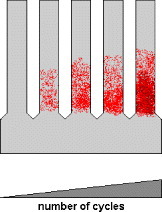
Figure 2 Schematic showing the expected fatigue damage formation along the cantilevers with increasing number of cycles.
High-throughput fatigue testing setup
Following the method described in the previous section, we have developed a novel experimental setup that allows us to obtain an S–N diagram for each cantilever by observing the propagation of the fatigue damage along the long axis of a coated cantilever. A possible approach to fatigue measurements using a vibrating cantilever was proposed by Wang et al [Citation24]. They investigated the frequency shift due to fatigue damage in Cu–Nb self-supported thin films and were mainly interested in fatigue crack initiation. In our method, thin films are attached to a Si substrate, and their local damage is detected by optical reflectivity.
The setup consists of the actuation part, the sample and the optical path. Two setups with different optical principles were implemented (figure ). Vibration is induced by a piezoelectric actuator (Physik Instrumente, Waldbronn, Germany) with a travel range of 90 μm. The actuator is attached to an x–z stage, which allows automated scanning of the cantilever array. The cantilevers are aligned perpendicular to the motion of the piezoactuator. Therefore, the actuator can induce the bending of the cantilevers at the resonance frequency of the first bending mode. The resonance frequencies are tuned by gluing different weights to the free ends of the cantilevers. So, by choosing different masses for each individual cantilever, the resonance can be tuned to different frequencies and only one sample is tested at a time. The hardware and data transfer in the setup are controlled by a LabVIEW program (National Instruments).
Figure 3 Top-view schematics of fatigue testing setups: (a) camera-based setup; the piezoelectric actuator excites the sample (S) and the camera (Cam) detects the deflection from the side. (b) Area detector setup, where the displacement and reflectivity changes of the cantilever are monitored by measuring the reflected laser spot on the area detector.
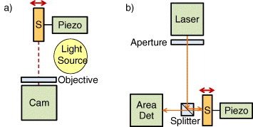
Figure (a) shows a schematic of the setup where a camera (6.6 Mpx CMOS, PixeLink) is used to measure the cantilever deflection from the side. The detection of the deflection can be improved by applying fluorescent paint to the edge of the cantilever and illuminating it by a black light source.
An edge detection algorithm is used to measure the deflection along the cantilever from the captured camera image. The image is taken with an exposure time corresponding to hundreds of cycles and therefore shows a blurred cantilever (figure (a)). Since the cantilever is slowest at its maximum deflection in each cycle, this deflection can be visualized at the resonance frequency of the cantilever, so that its edges can be detected more easily. The red lines in figure (a) represent the detected edges along the cantilever. The good agreement of the FE simulations described above with the experimental data (figure (a)) indicates the validity of the assumptions of our model, such as the linear elastic material properties.
Figure 4 (a) Optical image of a vibrating cantilever. The red lines indicate the edge detection positions. (b) Frequency sweep plot where deflection at a specific position along the cantilever is plotted vs. frequency. The excitation amplitude of the actuator was 3.6 μm. (c) Frequency sweep plot illustrating the normalized resonance peaks of two cantilevers with different weights glued to their ends.
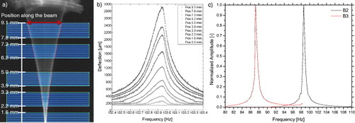
The measured deflections along the cantilever are plotted versus frequency in figure (b). The resonance frequency can be deduced precisely from the maximum in deflection at all positions along the cantilever. The advantage of this setup is that the deflection can be measured at any position of the cantilever.
Only one cantilever was tested at a time by tuning the piezo actuator to the corresponding resonance frequency. The FWHM of the resonance peaks is smaller than 1 Hz and the amplitude drops to less than 5% of the maximum at 5 Hz above or below the resonance frequency (figure (c)). These parameters were controlled beforehand to ensure that the out-of-tune cantilevers are not damaged during the cyclic loading of the cantilever under investigation.
In the second setup (figure (b)), a laser (Lasiris, 635 nm) is directed onto the cantilever and the reflected beam is detected by an area detector (Analog, Spot On), which can measure the reflected laser beam position and intensity with up to 20 kHz. The cyclical displacement of the laser spot on the detector by vibrating the cantilever can be analyzed to control the maximum strain amplitude of the cantilever. Furthermore, a motorized x–z stage is used to scan the fatigued cantilever for a change in curvature and local reflectivity due to damage formation in the thin film. This allows the automated detection of the damage front along the cantilever.
Fabrication of the cantilever array wafer
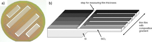
The cantilevers in the array had a variable length of 10–12 mm, a width of 1 mm and a thickness of 100–200 μm; they were separated by 1 mm. Double-side polished 4 inch (100) Si wafers (thickness ∼500 μm) were thermally oxidized, resulting in a 300 nm-thick silicon oxide layer. A 100 nm silicon nitride layer, used as the mask for the later KOH etching, was produced by low-pressure chemical vapor deposition. This silicon nitride film also compensates stresses in the substrate induced by the silicon oxide layer, resulting in flat cantilevers. Furthermore, it serves as a diffusion barrier to prevent a reaction between Si and the films of interest. Photolithography on the backside was performed using the AZ1518 photoresist and a SUSS MA6 mask aligner. The structures were aligned in the [100] direction to produce cantilevers with perpendicular sidewalls. The pattern transfer (local removal of silicon nitride and silicon oxide) was performed by reactive ion etching, and the photoresist was removed in oxygen plasma. A KOH wet etch process (30% KOH at 80 °C) was applied for the final release of the cantilevers with a duration dependent on the cantilever thickness. Figure (a) shows a photograph of a micro-machined Si wafer. Lines were etched on the wafers to facilitate their breaking into four cantilever arrays.
Figure 5 (a) Micro-machined Si wafer with four cantilever arrays (16 and 32 cantilevers); (b) schematic of the cantilever array. The deposited films form a continuous composition gradient on the cantilevers.
Fabrication of thin films
Cu films of 1 μm thickness were deposited on the fabricated cantilever arrays using a combinatorial rf magnetron sputtering system (DCA, Finland). Deposition was carried out in Ar atmosphere; the substrates were not heated and were kept at ground potential. A Cu target of 100 mm diameter and 99.999% purity was positioned 140 mm above the substrate. The base pressure prior to deposition was 2.66×10⁻⁶ Pa, while the pressure during deposition was adjusted between 0.266 and 1.999 Pa. The sputter power was kept at 200 W. To improve the adhesion of Cu films to the substrate, we have applied rf bias with a power ranging from 25 to 50 W. After the deposition, the film thickness was measured using a mechanical profilometer (Ambios, XP2).
The following approach can be used for the future deposition of materials libraries on cantilever arrays. Binary films can be fabricated by either co-deposition, where two elements are simultaneously sputtered from two targets, or sequential wedge-type multilayer deposition. The resulting composition depends on the geometry of the chamber and the sputtering rates of the targets. The sequential deposition allows the deposition of nanoscaled wedge-type layers where the compositional gradients are adjusted by the use of moving shutters. The long axes of the cantilevers are oriented at 90° to the gradient direction to minimize the compositional variation over one cantilever. A metallic or Si shadow mask is applied for individual deposition on a cantilever array within the wafer. For ternary systems, it is beneficial to deposit pseudo-binary composition spreads on the cantilever array using the wedge-type multilayer approach, i.e., a repeated deposition of opposing wedge-type films of two elements with an intermediate, uniform layer of the third element [Citation14].
Results and discussion
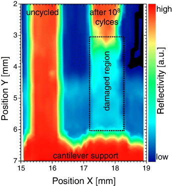
The new setup was tested on a 1 μm thick Cu film with grain sizes in the range of 200–400 nm. The cantilever with an attached weight had a resonance frequency of 467 Hz and a calculated maximum stress amplitude of about 300 MPa at the fixed end of the cantilever. During a 108 cycle test, the resonance frequency increased by less than 1 Hz. In contrast, the intensity of the laser spot on the area detector decreased by about 70% due to the fatigue-induced roughening and subsequent decrease in reflectivity of the film surface. As described above, an x–z stage can be used to scan the cantilever array while measuring the intensity of the reflected laser beam, and the 2D scan of the reflectivity allows us to determine the position of the fatigue-induced damage front (figure ). The 2D scan shows two cantilevers and the cantilever support. The right cantilever has been cycled in resonance, to damage the film deposited on it, while the left cantilever remains in the as-deposited state. For the right cantilever, the damage front has reached a distance of 3 mm from the support, which is equivalent to a stress amplitude of 190 MPa. This means that the 1 μm Cu thin film fails at a stress of 190 MPa after 108 cycles.
Figure 6 2D scan of the relative reflectivity. Left part shows an undamaged cantilever with high reflectivity, which has not been cycled in resonance. A strong decrease in the reflectivity is observed after 108 cycles in resonance in the right cantilever.
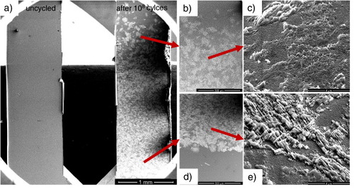
After the test, micrographs of the same cantilevers were taken using a scanning electron microscope (SEM, figure ). Figure (a) compares the as-deposited and fatigued thin films. The out of tune cantilever has a smooth surface, whereas the cycled Cu thin film shows severe fatigue damage, which varies along the length of the cantilever, as expected. Figures (b)–(e) show the regions near the free and fixed ends of the cantilever, respectively. Many closely spaced extrusions are visible in the highly stressed region (figures (d) and (e)) near the fixed end; the extrusions are less abundant and pronounced near the free end of the cantilever.
Figure 7 SEM images showing a 1 μm-thick Cu film: uncycled (a, left) and after 108 cycles (a, right), and extrusion formation in the regions with low (b,c) and high (d,e,) stress.
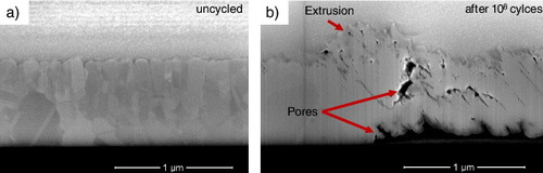
The damage morphology observed here is somewhat different from what was described in [Citation5]. Zhang et al observed mainly grain boundary cracking and almost no extrusion formation for 1 μm thin films with grain sizes smaller than the film thickness. They attributed this to inhibited dislocation creation and motion in the small volume. In our Cu thin films, clear extrusions are observed over a large area of many grains. As the grain size has increased after cycling, it can be argued that grain growth is a prerequisite for extrusion formation since more volume is created to allow dislocation structures to form. Note that we conducted fatigue tests in the HCF regime, which might have different mechanisms of fatigue damage. Besides the surface damage, we also observed the microstructure of the cross section (figure ). Figure (a) shows the cross-section of the as-deposited Cu film, which was prepared using a focused ion beam microscope. After 108 cycles (figure (b)), the thin film displays cracks and pores at the interface to the underlying substrate, which is similar to previous observations [Citation5, Citation9]. Further electron microscopy observations are necessary to clarify the fatigue damage mechanisms.
Figure 8 Cross sections of a Cu thin film: (a) as-deposited, (b) cut through an extrusion of a Cu thin film after 108 cycles. Note the pore formation inside the film and along the interface to the underlying substrate.
Summary and outlook
We have presented a novel high-throughput methodology which allows measuring fatigue lifetime and damage formation in metallic thin films on Si cantilevers. The use of a cantilever array allows fatigue testing of thin films with a range of stress amplitudes. Scanning the film reflectivity during fatigue testing allows detection of the damage front. The stress level at the position of the damage front can be calculated from the measured absolute deflection of the cantilever by FE simulation. By plotting the damage front position versus the applied cycle number, a lifetime diagram can be rapidly constructed for each cantilever.
This new approach will be used in the future to study the fatigue properties of thin films libraries deposited on cantilever arrays, and the materials of interest include binary (Al–Cu, Al–Mg, Al–B) and ternary (Al–Cu–Mg, Al–Mg–Si) alloys. The new method will enable the reliable and rapid correlation of compositional and structural data with the fatigue behavior.
Acknowledgments
We thank the German Research Foundation (DFG) for funding (SFB 499 N01, EB 362/3-1, LU 1175/6-1) and Ewald Ernst, Benjamin Rupp, Sven Bundschuh, Alan Savan and Michael Ehmann for their support in the laboratory. MEMS processing was partly performed by the Caesar Micro Systems Technology Group, Bonn, Germany.
Related Research Data
References
- NixW 1989 Metall. Mater. Trans. A 20 2217 http://dx.doi.org/10.1007/BF02666659
- ArztE 1998 Acta Mater. 46 5611 http://dx.doi.org/10.1016/S1359-6454(98)00231-6
- SubraS 1998 Fatigue of Materials Cambridge Cambridge University Press
- WöhlerA 1860 Z. Bauwesen 10
- ZhangG PVolkertC ASchwaigerRWellnerPArztEKraftO 2006 Acta Mater. 54 3127 http://dx.doi.org/10.1016/j.actamat.2006.03.013
- ReadD T 1998 Int. J. Fatigue 20 203 http://dx.doi.org/10.1016/S0142-1123(97)00080-7
- SchwaigerRDehmGKraftO 2003 Phil. Mag. 83 693 http://dx.doi.org/10.1080/0141861021000056690
- WangDVolkertC AKraftO 2008 Mater. Sci. Eng. A 493 267 http://dx.doi.org/10.1016/j.msea.2007.06.092
- SchwaigerRKraftO 1999 Scr. Mater. 41 823 http://dx.doi.org/10.1016/S1359-6462(99)00231-6
- EberlCSpolenakRKraftOKubatFRuileWArztE 2006 J. Appl. Phys. 99 113501 http://dx.doi.org/10.1063/1.2189970
- ParkJ HMyungM SKimY J 2008 Sensors Actuators A 147 561 http://dx.doi.org/10.1016/j.sna.2008.06.003
- LiY PZhangG P 2010 Acta Mater. 58 3877 http://dx.doi.org/10.1016/j.actamat.2010.03.042
- LudwigACaoJBruggerJTakeuchiI 2005 Meas. Sci. Technol. 16 111 http://dx.doi.org/10.1088/0957-0233/16/1/015
- ZarnettaREhmannMSavanALudwigA 2010 Smart Mater. Struct. 19 065032 http://dx.doi.org/10.1088/0964-1726/19/6/065032
- ZarnettaRKönigDZamponiCAghajaniAFrenzelJEggelerGLudwigA 2009 Acta Mater. 57 4169 http://dx.doi.org/10.1016/j.actamat.2009.05.014
- TakeuchiIet al 2003 Nat. Mater. 2 180 http://dx.doi.org/10.1038/nmat829
- FamoduOHattrick-SimpersJAronovaMChangK-SOkazakiTFuruyaYKnaussLBenderskyLBiancanielloF 2004 Mater. Trans. 45 173 http://dx.doi.org/10.2320/matertrans.45.173
- Hattrick-SimpersJ Ret al 2008 Appl. Phys. Lett. 93 102507 http://dx.doi.org/10.1063/1.2980034
- LudwigACaoJDamBGremaudR 2007 Appl. Surf. Sci. 254 682 http://dx.doi.org/10.1016/j.apsusc.2007.05.093
- LudwigACaoJSavanAEhmannM 2007 J. Alloys Compd. 446–447 516 http://dx.doi.org/10.1016/j.jallcom.2007.01.069
- WooN CNgB Gvan DoverR B 2007 Rev. Sci. Instrum. 78 072208 http://dx.doi.org/10.1063/1.2755779
- KimH-JHanJ-HKaiserROhK HVlassakJ J 2008 Rev. Sci. Instrum. 79 045112 http://dx.doi.org/10.1063/1.2912826
- LimS-HRaoraneDSatyanarayanaSMajumdarA 2006 Sensors Actuators B 119 466 http://dx.doi.org/10.1016/j.snb.2006.01.032
- WangY-CHoechbauerTSwadenerJ GMisraAHoaglandR GNastasiM 2006 Exp. Mech. 46 503 http://dx.doi.org/10.1007/s11340-006-7556-4