Abstract
This work describes novel surface-enhanced Raman scattering (SERS) substrates based on ferroelectric periodically poled LiNbO3 templates. The templates comprise silver nanoparticles (AgNPs), the size and position of which are tailored by ferroelectric lithography. The substrate has uniform and large sampling areas that show SERS effective with excellent signal reproducibility, for which the fabrication protocol is advantageous in its simplicity. We demonstrate ferroelectric-based SERS substrates with particle sizes ranging from 30 to 70 nm and present tunable SERS effect from Raman active 4-mercaptopyridine molecules attached to AgNPs when excited by a laser source at 514 nm.
1. Introduction
Surface-enhanced Raman scattering (SERS) has received a great deal of attention for its utility as a sensitive technique for chemical and biological analysis at the molecular level [Citation1–Citation4]. The high sensitivity of SERS is believed to be a result of the great enhancement of the Raman scattering cross section of molecules on metal nanoparticles. This phenomenon has been demonstrated to arise from two important factors: chemical enhancement (0–102) and electromagnetic enhancement (104–1012). The major contribution to the SERS enhancement comes from the electromagnetic enhancement mechanism, in which plasmon excitation in the particle creates an enhanced local electric field near the particle surface depending on the optical properties of metal nanoparticles in terms of size, shape, interparticle separation and dielectric environment [Citation5–Citation8].
Although SERS has been known for nearly four decades, the search for a suitable substrate is still an active area of research. An ideal SERS substrate should be reproducible while exhibiting high SERS enhancement over large areas at a low cost. Self-assembly techniques [Citation9–Citation11], nano-lithography techniques [Citation12–Citation15] and their combinations [Citation16–Citation19] have been employed to fabricate and optimize SERS substrates for detection of and discrimination between analytes. While techniques such as electron beam lithography are capable of the creation of high-quality arrays of metallic nanostructures, they often involve a fabrication with a multi-step lithography, leading to a time-consuming and high-cost process [Citation20]. Ferroelectric lithography is a time- and cost-effective technique which enables the creation of metallic nanostructures over large lateral sample sizes from millimeters to centimeters, and its surface assembly processes can be controlled with nanoscale precision [Citation21–Citation24].
Ferroelectric materials have reversible spontaneous polarization. Polarization inversion results in domain patterns with polar surfaces that exhibit surface-bound charges. The different domains have surfaces with different electronic properties including electron affinity [Citation25] and surface potential [Citation26, Citation27]. Ferroelectric LiNbO3 single crystal is favorable for the creation of high-quality patterns of metallic nanostructures due to its large polarization existing only along the crystallographic Z-axis. A number of studies have shown that silver nanoparticles (AgNPs) with nano- and microstructures can be created via photochemical reduction of Ag+ to Ago from an aqueous solution onto the domain surfaces of LiNbO3 [Citation21, Citation28–Citation33]. Upon above-bandgap illumination, photochemical deposition occurs on the polarized domains [Citation21, Citation31–Citation33] and domain boundaries [Citation28, Citation29] yielding silver nanoparticle micro-surfaces and nanowires, respectively. It has been demonstrated that the variation of deposition location is caused by factors including electric field distribution on LiNbO3, illumination wavelength and the ratio of Ag+ ion and photon flux [Citation34, Citation35]. Although ferroelectric lithography has been studied for years, there are still many challenges in fabricating metallic nanostructures with highly uniform and size-controlled nanoparticles. As a result, very limited research has been performed on SERS applications of metallic nanostructures on ferroelectrics. Recently, Carville et al [Citation36] demonstrated a chemical patterning technique via proton exchange to modulate the polarization at the surface of LiNbO3 crystal which can be used as a template for fabrication of silver nanostructures. The AgNPs deposited in the proton diffusion region (1.5 μm width) below the patterning mask showing an enhanced particle density at the boundary between LiNbO3 and proton-exchanged regions. The patterned AgNP arrays have been further demonstrated to be plasmon active [Citation37]. Compared to the chemical patterning technique, the electric poling is a well-established technique which allows the creation of periodically poled LiNbO3 (PPLN) with a controllable period of a few tens of microns repeated across the sample. Metallic nanoparticle arrays can be fabricated via photochemical deposition on polarized domain surfaces of the PPLN, which enable SERS to detect low concentrations of molecules. Our previous work has confirmed that AgNP arrays fabricated on LiNbO3 domain surfaces can effectively detect the multifunctional fusion protein (MBP–GFP–AgBP) absorbed on the AgNPs showing enhanced Raman spectra of the protein [Citation31].
In this work, we focus on the fabrication of large-scale metallic nanoparticle arrays with uniform and size-controlled AgNPs based on PPLN templates, which can be used as tunable and highly reproducible SERS substrates. With an appropriate above-bandgap illumination and an optimum ratio of Ag+ ion and photon flux, we are able to generate AgNP arrays via the fabrication of uniform AgNPs over the positively poled (+ Z) domain surfaces (∼ 15 μm width). The size of AgNPs is controlled by varying the illumination time while maintaining the ratio of the Ag+ ion and photon flux. SERS results indicate tunable Raman spectra of 4-mercaptopyridine (4MP) by tuning the size of AgNPs. Small deviation (∼ 7%) in SERS signals collected from random spots across the AgNP arrays and large-area uniformity of Raman enhancement seen from the SERS mapping demonstrated highly reproducible large-scale ferroelectric-based SERS substrates.
2. Experimental details
2.1. Preparation of LiNbO3 samples
The LiNbO3 samples were cut from a 0.5 mm-thick Z-cut LiNbO3 wafer (Oxide Ltd, Japan). Polarization inversion was performed with a conventional electric poling technique using a patterned photoresist covered by a metal film on the positive surface and a continuous liquid electrode of LiCl aqueous solution on the negative surface. PPLN was then diced into pieces of 5 × 8 mm2 (Swing Ltd, Japan) and were used as photochemical deposition templates after ultrasonic cleaning in acetone, alcohol and deionized (DI) water sequentially.
2.2. Fabrication of SERS substrate
Photochemical deposition was performed by placing a 1 mM AgNO3 aqueous solution over the PPLN templates under above-bandgap light illumination. A UV spot light source (Hamamatsu 5662) equipped with a 200 W mercury–xenon lamp and a 313 nm bandpass filter was used for the illumination with an intensity of 120 mW cm2. The illumination time was varied from 15 to 25 min in order to create a variety in the sizes of photochemically deposited AgNPs. After the deposition, the samples were rinsed in DI water and then blown dry with nitrogen. A tapping mode atomic force microscope (AFM) (Asylum Research) was used to examine the morphology of as-deposited AgNPs.
2.3. Raman spectroscopy
4MP was used as a probe molecule for SERS measurement. The substrates were immersed in a 3 mM 4MP aqueous solution for 3 h to form a 4MP monolayer onto the AgNPs. They were then taken out, rinsed with DI water to remove any unabsorbed 4MP molecules, and dried with a stream of air. Raman spectroscopy was conducted using a Renishaw InVia Raman spectrometer attached to a Leica DMLM upright microscope. A 50 × (NA = 0.8) objective was used to focus the laser on a target area and to collect the scattering light from the sample surface. A spot of 2 μm diameter and 514 nm laser excitation from a diode laser at a power of 3 mW was used to irradiate the sample surfaces. The irradiation time for SERS spectra was 10 s.
2.4. Absorption spectroscopy
UV–vis absorption spectra were recorded on a Perkin-Elmer model Lambda 900 UV–Vis–near-IR spectrophotometer. 30, 50 and 70 nm AgNPs for absorption measurements were photochemically deposited on the positively poled LiNbO3 surfaces and measured using bare LiNbO3 substrate as reference.
3. Results and discussion
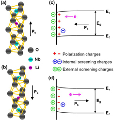
Essential to the ferroelectric lithography is the use of ferroelectric materials, which can be patterned as charged domain surfaces corresponding with polarizations. LiNbO3 single crystal is characterized by hexagonal symmetry with its polarization only along the crystallographic Z-axis resulting in two possible polarization orientations with 180° domain boundaries (figures (a) and (b)). Unlike ferroelectric materials such as lead zirconium titanate (PZT) having a large density of defects (1014 cm−2) due to oxygen vacancies, LiNbO3 single crystal has a low defect density (1012 cm−2) leading to a weak internal screening and small band bending near the surface (figures (c) and (d)). Therefore, when the LiNbO3 exposes to an aqueous AgNO3 solution, polarization charges are screened mainly by external charged ions and molecules from the solution forming an electrical double layer [Citation38]. On the +Z domain surface, the first screening layer consisting of NO3− ions, free electrons and polarized H2O molecules is compensated by the second layer of positively charged presences including Ag+ ions [Citation39]. The same screening mechanism occurs on the negatively poled (− Z) domain surface. Under an above-bandgap illumination (> 3.9 eV), the photon absorption process produces electron–hole pairs near the surface. Note that the small band bending in LiNbO3 results in a small internal field which cannot be a driving force of carrier transport. Glass et al [Citation40] attributed the photogalvanic current in LiNbO3 crystals under zero external field to an asymmetric charge transfer process and Franck–Condon shifts of the excited ions along the polar axis. The photoexcited electrons move preferentially in the +Z direction, which may lead to a dissociation of negative screening charges from the surface and thus enable transport of the Ag+ ions to the surface. As a result, reaction of Ag+ + e = Ag0 occurs preferentially on the +Z surface, and the reduced Ag atoms nucleate and grow continuously to form larger particles. There is also the possibility of a small amount of Ag atom nucleation on the −Z domain surface due to electron diffusion; however, this can be suppressed by adjusting the ratio of Ag+ ion and photon flux.
Figure 1. Schematic diagram of crystal structure and associated band structure of LiNbO3. (a), (b) Polarization orientation induced by a displacement of Nb within the same octahedron and a motion of Li from one octahedron to the adjacent vacant octahedron. (c), (d) Small band bending for LiNbO3 with dominated external screening.
The Ag+ ion flux, Ji, depends on the concentration and mass of the solute, which can be expressed as
1
where v0 is the average velocity of a solution particle toward a surface and C0 is the particle concentration in the bulk AgNO3 solution. The average velocity, v0, is considered as the surface collision velocity within a mean free path distance from the surface [Citation41]. This velocity is not dependent on solvent properties such as viscosity; thus it can be approximated as
2
where k is the Boltzmann constant, T is the temperature in kelvins and m is the mass of the particle in the solution.
The photon flux, Jp, is determined by the light wavelength and illumination intensity
3
where I0 is the illumination intensity, λ is the light wavelength, h is Planck's constant and c is the speed of light.
The present results of photochemical deposition were produced using a 1 mM AgNO3 aqueous solution and a 313 nm UV light with an intensity of 120 mW cm2. According to equations (Equation11 ) and (Equation2
2 ), the Ag+ ion flux can be calculated to be 1021 cm−2 s−1, and the photon flux of 1017 cm−2 s−1 is determined from equation (Equation3
3 ), resulting in a ratio of Ag+ ion and photon flux of 104. This is an optimum value for the generation of AgNPs on the +Z domain surface, which is in good agreement with reported data from Sun et al [Citation34].
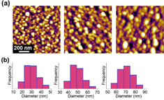
Figure (a) shows a simple setting of the ferroelectric photochemical reaction. The dark field image (figure (b)) displays a large area of AgNP arrays fabricated by the photochemical deposition. The AFM photographic (figure (c)) and three-dimensional (3D) (figure (d)) images demonstrate the distribution of AgNPs deposited over the +Z domain surfaces. To generate AgNPs of different sizes, we tuned the illumination time while keeping the same ratio of Ag+ ion and photon flux. The size of the AgNPs was determined from the visual analysis of AFM topographic images. Single particle diameter is determined from the AFM cross-section profile across the center of the particle. The average particle diameter is calculated statistically with areas of 1 × 1 μm2 at ten different regions in the pattern for each sample. Figure (a) displays AFM topographic images of the AgNPs with average diameters of 30, 50 and 70 nm, which were produced at the UV illumination time of 15, 20 and 25 min, respectively. Size distribution of the AgNPs is shown in histograms (figure (b)), corresponding to the AFM topographic images (figure (a)).
Figure 2. (a) Schematic diagram of photochemical reaction. (b) Dark field image showing large-scale AgNP arrays fabricated via the photochemical deposition. (c) Zoom-in image of AgNP arrays from AFM topography. (d) 3D AFM image of the same area as shown in (c).
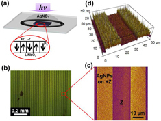
Figure 3. (a) AFM topographic images of photochemically deposited AgNPs at the average diameter of 30, 50 and 70 nm, generated with different illumination time of 15, 20 and 25 min, respectively. (b) Size distribution of the AgNPs on LiNbO3, corresponding with the above AFM topographic images. The scale bar in (a) applies to all three images.
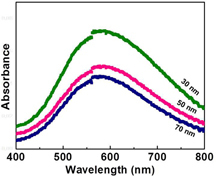
UV–vis spectrum shows far-field properties related to extinction efficiencies. It is sensitive to the formation of AgNPs because AgNPs exhibit an intense absorption peak due to the local surface plasmon resonance. Figure shows the UV–vis spectra of the AgNPs of three different sizes. The increase in absorbance indicates the increase in the number density of AgNPs, consistent with the AFM characterization as shown in figure . However, no visible shift of the absorption peaks was observed in figure , implying that the far-field absorption spectral behavior cannot provide information on the trend of the enhancement. A recent finite-difference time-domain electromagnetic simulation shows that while the far-field reflectance spectra remain the same, the near-field electric field distribution and the intensity vary when the incident light polarization changes [Citation42]. Another recently published result from Altun et al [Citation43] demonstrates that SERS-active substrates made by gold on hafnia-coated carbon nanotubes exhibit strong SERS effect but do not show a visible plasmon resonance in the far field.
Figure 4. UV–Vis absorption spectra of the given AgNPs of three different sizes on the LiNbO3 substrates.
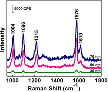
The AgNP arrays fabricated by photochemical deposition on the PPLN are then used as ferroelectric-based SERS substrates. SERS properties of the substrates were evaluated using 4MP, a well-known probe molecule for SERS study because it has a large scattering cross section and forms a monolayer on metal surfaces, making the estimate of surface coverage convenient [Citation14, Citation44]. A 4MP monolayer was absorbed onto the AgNPs by immersing the substrates into a dilute aqueous solution of 4MP. Figure shows the SERS spectra of 4MP recorded on the ferroelectric-based SERS substrates with the AgNPs in the average diameter of 30, 50 and 70 nm. All of the Raman bands match well with the characteristics of the Raman spectrum of 4MP [Citation45]. The bands at 1004 and 1096 cm−1 are assigned to the ring breathing mode. The band at 1215 is assigned to the C–H bending mode, and 1576 and 1610 cm−1 are assigned to the modes. We attribute the Raman enhancement to the non-uniform coupling (narrow gaps) of nanoparticles. The gap size is constrained by Ag atom nucleation density and particle size. The nucleation density depends mainly on the ratio of Ag+ ion and photon flux, which is kept at a constant value in this work. As the particles grow larger, the gap between particles becomes narrower. The smallest size may have a small local electric field due to a relatively large gap between the particles, thus the signal enhancement is low for the substrate with 30 nm AgNPs. The enhancement performance of the substrate, however, significantly improved as the size of the nanoparticles was increased. The substrate with 70 nm AgNPs exhibits the highest enhancement among the given three samples. It is well known that the major mechanism of SERS is electromagnetic enhancement, which involves enhancements in the field intensity as a result of plasmon resonance excitation. In this mechanism, the enhancement factor (EF) at probe molecules is approximated by EF = |E|4, where E is the local electric field enhancement factor at the incident frequency [Citation46]. The high enhancement produced in this work is considered as a largely enhanced local electric field induced by a narrow gap from the substrate with 70 nm AgNPs.
Figure 5. SERS spectra of 4MP absorbed on the SERS substrates with AgNPs of different sizes on the LiNbO3 substrates. All SERS spectra were measured under the 514 nm excitation. The laser power focused on samples was 3 mW. The acquisition time was 10 s.
To estimate the enhancement ability of the ferroelectric-based SERS substrates, we calculated the enhancement factor by comparing the intensity of the appropriate 4MP peak (1096 cm−1) measured in the SERS experiments with the intensity of the corresponding peak measured from a bulk sample of 4MP. The SERS enhancement factor is defined as following:
4
where Isurf is the intensity of the SERS spectrum of the surface-adsorbed 4MP molecules, Ibulk is the intensity from the bulk 4MP molecules in the conventional Raman spectrum and Nsurf and Nbulk are the number of molecules adsorbed on the SERS substrates and in the bulk sample, respectively. To acquire the Raman spectrum of the bulk 4MP, we used a 0.5 M aqueous solution. In order to determine the number of molecules that contributed to the Ibulk signal, we had to determine the confocal depth profile of our microscope [Citation47]. For the optical configuration and microscope employed in this work, the 514 nm laser was focused into a circle with a diameter of 2 μm, and the confocal depth was 10 μm giving a focal volume of 0.03 pl, and thus Nbulk, for a 0.5 M solution, would be 9 × 10⁹ 4MP molecules. The Nsurf was estimated to be ∼3.9 × 10⁶ per laser spot size by adapting the packing density of 6.8 × 10¹⁴ molecules·cm−2 [Citation48]. Using the 1096 cm−1 band, the Ibulk was 110. From these numbers, the EF value was calculated as 3.8 × 10⁶, 2.5 × 10⁶ and 3.6 × 10⁵ for the substrates with 70, 50 and 30 nm AgNPs, respectively. A rough estimate of the EF gives a direct indication about the SERS trend observed.
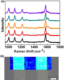
Applications of SERS are often limited by challenges in reproducibility in the SERS signals. A significant advantage of the ferroelectric-based SERS substrates is their large-scale uniformity of Raman enhancement, and in turn high reproducibility of probe molecules owing to the enhanced local electric field. To evaluate this capability, SERS spectra were taken from five randomly chosen positions separated by a few micrometers across the AgNP arrays with the three different nanoparticle sizes. Figure (a) shows the data recorded from the 50 nm AgNPs substrate. The spectra are consistent in shape, and the relative standard deviation (RSD) in the spot-to-spot intensity of Raman band (1096 cm−1) of 4MP is approximately 7%, which is comparable with the recently reported commercialized substrate but at a much lower SERS signal intensity [Citation49]. We further detected the uniformity of Raman enhancement from a two-dimensional point-by-point SERS mapping of 4MP molecules. The SERS mapping was achieved in an area of 50 × 16 μm2 at a vibration peak of 1096 cm−1. Figure (b) shows SERS mapping image overlapped upon bright field optical image of the focused sample region on the 50 nm AgNPs substrate. Large light blue regions indicate areas of high enhancement and the RSD in intensities of Raman band (1096 cm−1) of 4MP is approximately 10%. Coupling with the tenability and the reproducibility, ferroelectric-based SERS substrates provide a promising platform in analytical studies. Moreover, its simplicity in fabrication will lead to a cost-effective manufacturing.
Figure 6. (a) Reproducibility in SERS signals across the AgNP arrays. The signals were collected from random positions separated by a few micrometers on the substrate with 50 nm AgNPs. (b) Two-dimensional SERS mapping of 4MP absorbed on the 50 nm AgNPs substrate showing a large-scale uniformity of SERS signals across the substrate.
4. Conclusion
In summary, we have made ferroelectric-based SERS substrates that show tunable and highly reproducible SERS effect over large areas. The ferroelectric-based SERS substrates were self-assembled with AgNP arrays by making use of the unique properties of LiNbO3, including polarization-induced surface charges, screen states and photogalvanic effect. Varying the size of the AgNPs allows the tuning of the gap between nanoparticles and thus the local enhanced electric field and the SERS enhancement factor was maximized for a given substrate with 70 nm AgNPs. Moreover, the ferroelectric-based SERS substrates were demonstrated to have high reproducibility across the AgNP arrays with small signal deviation and large-scale uniformity of Raman enhancement, overcoming a common drawback of the most of existing SERS substrates. The tenability, high reproducibility and simplicity in fabrication make the ferroelectric-based SERS substrate a viable contender for SERS, both in fundamental studies and in analytical fields.
Acknowledgments
This work was supported by the World Premier Institute Initiative for Materials Nanoarchitectonics (MANA) in National Institute for Materials Science, Japan. XL acknowledges Dr S Takekawa for help preparing the PPLN samples and Dr H Xin for help with UV–Vis absorption spectra measurements. Part of this work was conducted at the University of Washington NanoTech User Facility, a member of the NSF National Nanotechnology Infrastructure Network (NNIN).
References
- BellS E JSirimuthuN M S 2006 J. Am. Chem. Soc. 128 15580 10.1021/ja066263w
- KneippKKneippHItzkanIDasariR RFeldM S 1999 Chem. Rev. 99 2957 10.1021/cr980133r
- NieS MEmeryS R 1997 Science 275 1102 10.1126/science.275.5303.1102
- SackmannMMaternyA 2006 J. Raman Spectrosc. 37 305 10.1002/jrs.1443
- XuH XAizpuruaJKallMApellP 2000 Phys. Rev. E 62 4318 10.1103/PhysRevE.62.4318
- HicksE MZouS LSchatzG CSpearsK GVan DuyneR PGunnarssonLRindzeviciusTKasemoBKallM 2005 Nano Lett. 5 1065 10.1021/nl0505492
- SherryL JChangS HSchatzG CVan DuyneR PWileyB JXiaY N 2005 Nano Lett. 5 2034 10.1021/nl0515753
- ZhangX YHicksE MZhaoJSchatzG CVan DuyneR P 2005 Nano Lett. 5 1503 10.1021/nl050873x
- BaumbergJ JKelfT ASugawaraYCintraSAbdelsalam M EBartlettP NRussellA E 2005 Nano Lett. 5 2262 10.1021/nl051618f
- MuCZhangJ PXuD S 2010 Nanotechnology 21 015604 10.1088/0957-4484/21/1/015604
- WangHLevinC SHalasN J 2005 J. Am. Chem. Soc. 127 14992 10.1021/ja055633y
- HatabN AHsuehC HGaddisA LRettererS TLiJ HEresGZhangZ YGuB H 2010 Nano Lett. 10 4952 10.1021/nl102963g
- WardD RGradyN KLevinC SHalasN JWuY PNordlanderPNatelsonD 2007 Nano Lett. 7 1396 10.1021/nl070625w
- YuQ MGuanPQinDGoldenGWallaceP M 2008 Nano Lett. 8 1923 10.1021/nl0806163
- YuQ MBraswellSChristinBXuJ JWallaceP MGongHKaminskyD 2010 Nanotechnology 21 355301 10.1088/0957-4484/21/35/355301
- AlexanderK DHamptonM JZhangS PDhawanAXuH XLopezR 2009 J. Raman Spectrosc. 40 2171 10.1002/jrs.2392
- LeeS YHungLLangG SCornettJ EMayergoyzI DRabinO 2010 Acs Nano 4 5763 10.1021/nn101484a
- StoerzingerK AHasanWLinJ YRoblesAOdomT W 2010 J. Phys. Chem. Lett. 1 1046 10.1021/jz100095b
- YanBThubagereAPremasiriW RZieglerL DDal NegroLReinhardB M 2009 ACS Nano 3 1190 10.1021/nn800836f
- KleinmanS LFrontieraR RHenryA IDieringerJ AVan DuyneR P 2013 Phys. Chem. Chem. Phys. 15 21 10.1039/c2cp42598j
- LiuXKitamuraKTerabeKHatanoHOhashiN 2007 Appl. Phys. Lett. 91 044101 10.1063/1.2759472
- LiD BBonnellD A 2008 Annu. Rev. Mater Res. 38 351 10.1146/annurev.matsci.37.052506.084303
- BonnellD AKalininS VKholkinA LGruvermanA 2009 MRS Bull. 34 648 10.1557/mrs2009.176
- GiocondiJ LRohrerG S 2001 Chem. Mater. 13 241 10.1021/cM00890h
- YangW CRodriguezB JGruvermanANemanichR J 2004 Appl. Phys. Lett. 85 2316 10.1063/1.1790604
- KalininS VBonnellD A 2001 Phys. Rev. B 63 125411 10.1103/PhysRevB.63.125411
- LiuX YKitamuraKTerabeK 2006 Appl. Phys. Lett. 89 132905 10.1063/1.2358115
- HansonJ NRodriguezB JNemanichR JGruvermanA 2006 Nanotechnology 17 4946 10.1088/0957-4484/17/19/028
- HaussmannAMildePErlerCEngL M 2009 Nano Lett. 9 763 10.1021/nl8033784
- DunnSTiwariD 2008 Appl. Phys. Lett. 93 092905 10.1063/1.2978195
- HnilovaMLiuXYucaEJiaCWilsonBKaratasA YGresswellCOhuchiFKitamuraKTamerlerC 2012 ACS Appl. Mater Int. 4 1865 10.1021/am300177t
- LiuX YHatanoHTakekawaSOhuchiFKitamuraK 2011 Appl. Phys. Lett. 99 053102
- LiuX YOhuchiFKitamuraK 2008 Funct. Mater Lett. 1 177 10.1142/S1793604708000344
- SunYEllerB SNemanichR J 2011 J. Appl. Phys. 110 084303 10.1063/1.3647752
- SunYNemanichR J 2011 J. Appl. Phys. 109 104302 10.1063/1.3580509
- CarvilleN CManzoMDammSCastiellaMCollinsLDenningDWeberS A LGalloKRiceJ HRodriguezB J 2012 ACS Nano 6 7373 10.1021/nn3025145
- DammSCarvilleN CRodriguezB JManzoMGalloKRiceJ H 2012 J. Phys. Chem. C 116 26543 10.1021/jp310248w
- HendersonDBodaD 2009 Phys. Chem. Chem. Phys. 11 3822 10.1039/b815946g
- JonesP MDunnS 2009 J. Phys. D: Appl. Phys. 42 065408 10.1088/0022-3727/42/6/065408
- GlassA MLindeD V DNegranT J 1974 Appl. Phys. Lett. 25 233 10.1063/1.1655453
- AndersenO SFeldbergS W 1996 J. Phys. Chem. 100 4622 10.1021/jp952687t
- WangD QYuX LYuQ M 2012 Nanotechnology 23 405201 10.1088/0957-4484/23/40/405201
- AltunA OYounS KYazdaniNBondTParkH G 2013 Adv. Mater 25 4431 10.1002/adma.201300571
- McLellanJ MXiongY JHuMXiaY N 2006 Chem. Phys. Lett. 417 230 10.1016/j.cplett.2005.10.028
- BaldwinJ AVlckovaBAndrewsM PButlerI S 1997 Langmuir 13 3744 10.1021/la960719d
- SchatzG CYoungM AVan DuyneR P 2006 Top. Appl. Phys. 103 19
- CaiW BRenBLiX QSheC XLiuF MCaiX WTianZ Q 1998 Surf. Sci. 406 9 10.1016/S0039-6028(97)01030-3
- HaynesC LVan DuyneR P 2003 J. Phys. Chem. B 107 7426 10.1021/jp027749b
- DinishU SYawF CAgarwalAOlivoM 2011 Biosens. Bioelectron. 26 1987 10.1016/j.bios.2010.08.069