
Abstract
This review describes a series of representative synthesis processes, which have been developed in the last two decades to prepare silicon quantum dots (QDs). The methods include both top-down and bottom-up approaches, and their methodological advantages and disadvantages are presented. Considerable efforts in surface functionalization of QDs have categorized it into (i) a two-step process and (ii) in situ surface derivatization. Photophysical properties of QDs are summarized to highlight the continuous tuning of photoluminescence color from the near-UV through visible to the near-IR range. The emission features strongly depend on the silicon nanostructures including QD surface configurations. Possible mechanisms of photoluminescence have been summarized to ascertain the future challenges toward industrial use of silicon-based light emitters.
Introduction
Nanostructured materials with precisely controlled structures as seen in nanotubes [Citation1], nanoparticles [Citation2], nanosheets [Citation3], nanofilm [Citation4] and nanoporous material [Citation5] have put forward many innovations in current science and technology. Their unique exciting structures and properties have motivated increasingly active research in various fields. Among them, quantum sized materials with various new functions based on well-defined physics have gained a huge amount of attention from the scientific community [Citation6–Citation8]. In semiconductor quantum dots (QDs), photoluminescence (PL) occurs when an electron and a hole recombine to produce a photon. In direct bandgap semiconductor QDs, the electron and the hole are positioned at the same point (crystal momentum value k is the same) in the Brillouin zone, resulting in efficient radiative recombination across the bandgap and consequently short lifetimes at the nanosecond level. Additively in semiconductor QDs, the appearance of the quantum confinement effect has opened up the amazing possibility of beautiful color tunability. Furthermore, the quantum confinement effect allows tuning of the emission color—the color tuning. As a result the archetypical CdSe and PbS QDs have shown great promise in various optoelectronic and biomedical devices [Citation9–Citation15]. Much effort has been made in recent decades and still a lot of research focuses on the luminescent properties and possible applications. However, in indirect bandgap semiconductors such as silicon and germanium, the bottom of the conduction band and the top of the valance band are not at the same point in the Brillouin zone [Citation16, Citation17]. Due to this, the radiative recombination across the bandgap needs phonons to conserve crystal momentum, making them inefficient emitters. But after the startling discovery of efficient emission from porous silicon by Canham in 1991, the scientific communities have directed their attention and effort to understanding the emission mechanism and possible future applications. After that discovery, silicon gained a lot of attention in the optoelectronic fields due to its number of added advantages and possible device applications including laser [Citation16–Citation21]. The added benefits of Si compared to the much-studied Cd or Pb are (i) good compatibility with the existing huge silicon electronics market, (ii) high abundance in the Earth's crust (second after oxygen), (iii) low toxicity and (iv) good cost performance. Approaches to improve the emission property of silicon can be grouped into two categories. Either the non-radiative recombination pathways are suppressed or the radiative recombination rate is enhanced. The use of nanostructures of silicon satisfies both criteria and it is probably the most promising avenue for achieving high luminescence efficiencies. After the Canham discovery of luminescence attributed to quantum confinement, much research on light emission from silicon has been conducted using porous silicon [Citation22], surface textured bulk silicon, silicon/silica superlattice, as well as silicon QDs fabricated through electrochemical etching and dispersion, silicon ion implantation plus annealing [Citation23], annealing of silicon oxide [Citation24] and hydrofluoric acid (HF) etching of silicon/silica nanostructures. However, when compared to the other luminescent nanostructures of silicon, colloidal silicon QDs offer the possibility of solution processing, shifted to the forefront of silicon research. Because of simple chemical treatment, good mechanical and chemical stability, and easily tailorable optoelectronic properties, colloidal silicon QDs have attracted much more attention. The colloidal stability of the QDs is attained by surface modification and ligands of various compositions. Surface functionalized silicon QDs have been explored to disperse in both organic and aqueous solvents using steric and charge stabilization synthetic strategies to achieve colloidal stability [Citation16, Citation25–Citation27].
Since then, many studies have been reported demonstrating synthesis and prototype applications of colloidally stable silicon QDs, displaying the room temperature luminescence. It has been shown that ligand-stabilized nanocrystals can be easily tuned to emit from the near-UV (NUV) through visible (VIS) to the near-IR (NIR) region with varying size and surface. These advantages make it an ideal material for solution processable applications [Citation28–Citation32]. However, the story does not end here. Unlike the direct bandgap semiconductors, the PL origin of the nanostructured silicon is still not very clear and is under debate. The yet-to-be-defined mechanism becomes a big obstacle for ease in access for emission tuning. As a result, research on luminescent silicon is very much important for fundamental studies too. A number of reports regarding emission are very interesting, but too counter-intuitive and even confusing to reach a unified conclusion. Based on the reported literature, emission of silicon QDs can be divided into two distinct regions. The first region is the emission range from NUV to aqua (λem = 300–500 nm), and another region is the green to NIR (λem = 500–950 nm) region. There is a discontinuity or wall between these two regions. Silicon QDs of these two emission ranges are prepared by fundamentally different preparation approaches. Unfortunately, there are no reports which break this barrier or discontinuity smoothly by a single preparation method. In the first decade after discovery, emission from silicon and related research was almost restricted to the red–NIR region. Emission wavelength was tuned by varying the size of QDs covered with amorphous silica shells. Later silicon QDs emitting in the ‘NUV–blue–green’ range have also emerged. While red–NIR emissions are commonly believed to appear due to the quantum confinement effect, NUV–blue emission is still controversial. According to previous papers, there are a variety of factors that affect the emission properties of silicon QDs, such as core size, stabilizers including surface monolayers, defect states and the interface of the oxide-shell/silicon-core [Citation23, Citation33–Citation36]. All phenomena must be considered in order to get an overall idea of the origin and to control emissions in the whole NUV–VIS–NIR range. As a result, the discovery of color-tunable emission from free-standing silicon QDs kindled the development and study of luminescent forms of silicon for its potential applications such as light-emitting diodes (LEDs), lasers, thermoelectric devices, solar cells and biomedical imaging [Citation16, Citation30–Citation34]. Furthermore, silicon is abundant, non-toxic and highly compatible with existing microelectronics technologies [Citation37]. Therefore, much attention has been given to the fabrication of optoelectronic devices using silicon QDs. This opens up a possibility to build a sustainable society that ideally uses resources and energy with high efficiency without causing damage to the environment or human health.
In this review we describe recent efforts on the synthesis of colloidal silicon QDs, and on the peculiar emissive properties, depending on the synthesis approaches and different surface chemistries. The mechanism of light emission in different spectral zones and the corresponding structures have been extensively reviewed to envision the challenges and prospects ahead in the field of silicon research.
Synthesis of silicon QDs
Nanomaterials are generally prepared by either one of two approaches, that is, top-down or bottom-up approaches. The top-down approaches use a larger macroscopic structure, which can be controlled externally to produce nanostructures. The bottom-up approaches include miniaturization of the material component at the atomic level with a further self-assembly process leading to nanostructures [Citation5]. Both approaches are available to prepare silicon QDs. A variety of procedures for fabricating free-standing silicon QDs have been reported and can be subdivided into another class of physical and chemical methods which includes both top-down and bottom-up approaches. Both physical and chemical approaches are useful in producing the nanostructures of silicon, and then proper surface chemistry provides solubility for a colloidal suspension of silicon QDs.
Physical methods generally involve the formation of silicon using ion implantation, laser ablation, magnetron sputtering and thermal evaporation. Chemical methods are also attractive because of the big opportunities in chemical flexibility and a huge scale of production. The most common methods within this class involve direct oxidation/reduction routes involving silicon precursors, thermal degradation of molecular silicon precursors in supercritical fluids, laser pyrolysis, plasma-assisted decomposition or thermolysis of sol–gel-derived silicon-rich oxides (SROs). Emission properties are very much dependent on the preparation process.
Top-down approach
We present herein two talented top-down approaches, that is, laser ablation and electrochemical etching. Both methods have been investigated since the earliest days of research on luminescent silicon.
Laser ablation.
Laser ablation is regarded as a clean technique during QD fabrication because of less production of waste [Citation38]. The first study on laser ablation for silicon nanostructures was carried out in 1991 by Okada and Iijima [Citation39]. The particles prepared were almost spherical, ranging from about 20 to 500 nm in diameter. High-resolution transmission electron microscopy (HRTEM) observations confirmed that the particles are composed of a crystalline phase, and the surfaces are oxidized with thin 1–2 nm amorphous oxide layers. The ablation was carried out using a wafer of silicon as the target under an argon or oxygen atmosphere; however, there was no information about the emission of those particles. Later in 1994, Werwa et al [Citation40] produced luminescent silicon QDs by some modification of the above approach. A wafer of silicon was ablated at a very low pressure of 10−8 Torr, yielding small silicon QDs of size range 2–3 nm with emission in the red region. Since then, with some modification to the preparation procedure, extensive studies have been performed [Citation41–Citation44]. Makimura et al [Citation45] produced luminescent silicon QDs using helium gas as the atmosphere for ablation. The approach was also used to study systematically silicon QDs prepared by laser ablation in non-equilibrium gas phases. Orii et al [Citation46] reported color tunable silicon QDs by changing the parameters of ablation in a helium gaseous environment. In that study, they successfully tuned the emission photon energies in the range 1.34 to 1.79 eV by size control of the QDs. Not only was laser ablation in a gaseous environment investigated, but also, to date, laser ablation of a solid target in a liquid environment has been widely used in the preparation of silicon QDs. Umezu and Senoo performed pulsed laser ablation of a silicon target in a liquid environment to prepare a silicon colloid solution. The emission photon energies from the colloidal solutions varied by changing the solvents: 2.9 and 3.5 eV for colloids prepared in water and hexane, respectively [Citation47]. Using a reactant as a solvent for liquid laser ablation, surface passivated free-standing silicon QDs were prepared in one step [Citation48]. Instead of a two-step process, which is a common method to produce organic-capped silicon QDs, the one-step process is called an ‘all-in-one’ strategy and is attractive because of automatic synthesis of organic-capped silicon QDs. Figure (A) illustrates the one-step process. A hydrogen-terminated silicon substrate immersed in 1-alkene was ablated with a laser beam. The silicon vapors and clusters produced by laser ablation assemble immediately to reduce the surface free energy, yielding the formation of nanocrystals. This facile route allows fabrication of colloidal silicon QDs in one step without waste. But it has disadvantages such as low product yield and less flexibility in tuning of the emission (restricted in the range from NUV to aqua) due to a rapid reaction of 1-alkene preventing the growth of nanocrystals [Citation49].
Figure 1 Schematic illustrations of the representative top-down approaches for the synthesis of free-standing (FS) silicon QDs: (A) liquid laser ablation and (B) electrochemical etching.
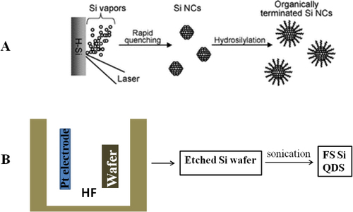
Electrochemical etching.
Another top-down approach is anodic oxidation, which is the most popular and has been widely used for silicon QD synthesis. Specifically, this is achieved by electrochemical etching of a wafer of silicon used as electrodes. This is the method that Canham used in 1991 to discover the visible luminescent silicon nanowires [Citation50–Citation52]. After that discovery, the procedure for generating colloidal suspensions of silicon with a luminescence character was reported in 1992 by Heinrich et al [Citation53]. A brief illustration is shown in figure (B) to explain this method. The wafers of n- or p-type silicon that had been electrochemically etched to form porous silicon can be ultrasonically dispersed into methylene chloride, acetonitrile, methanol, toluene or water solvent, forming a suspension containing silicon QDs. It is known that the product has irregular shapes of nanocrystals, and polydispersed nanocrystals ranging in size from the micrometer scale to nanometer scale. Later the Kauzlarich group developed a method to improve the size distribution by a slight modification as follows. Thin sections of porous silicon were ultrasonicated for a longer time and a 20 nm sieve was also used to remove larger crystallites from the colloids, resulting in the successful preparation of nanocrystals of narrow size distribution. In fact, HRTEM observations concluded that the sizes of nanocrystals are in the range of 2–11 nm. This is a very attractive route but it is not easy to control the size of nanocrystals at the single nanoscale [Citation54].
Bottom-up approach
A variety of chemical routes were demonstrated to produce silicon QDs, and most of routes are based on solution chemistry. The continuous tuning of the lights in the range from NUV through VIS to NIR are seen from the bottom-up approach.
Solution phase oxidation/reduction method.
Solution phase precursor reduction methods are attractive and widely studied in the preparation of metals and semiconducting nanostructures. One of the earliest attempts at using precursor reduction methods to prepare crystalline silicon was made in 1992 by Heath [Citation55]. The synthesis was based on the reduction of SiCl4 and RSiCl3 (R = hydrogen atom or octyl group) by sodium metal in a non-polar organic solvent at high temperatures (385 °C) and high pressures (> 100 atmospheres). Hexagonal-shaped crystalline silicon was formed. When trichlorosilane was employed, size control of the resulting silicon nanocrystals was not so easy. The size distribution covered a very broad range from 5 nm to 3 μm. In contrast, when trichlorooctylsilane was employed, the size distribution of the product was very narrow, and the average size was estimated at 5.5 ± 2.5 nm. Unfortunately, there was no information on the optical properties. Dhas et al [Citation56] modified the method to decrease the reaction temperature and pressure by developing a sonochemical method. The preparation was based on ultrasound-induced reduction of tetraethyl orthosilicate by sodium in toluene as a solvent at 70 °C. The product was porous silicon nanoparticles with diameters ranging from 2 to 5 nm, and the product showed the PL feature with an emission maximum at around 680 nm.
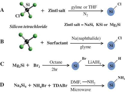
Figure (A) shows a low-temperature solution route reported in 1996 by Bley and Kauzlarich [Citation57]. In that reaction, the Zintl compound potassium silicide (KSi) was used to reduce SiCl4 in a tetrahydrofuran (THF) solution for 48–96 h under nitrogen at atmospheric pressure to produce crystalline silicon nanoparticles. Then, KSi was replaced by less reactive magnesium silicide (Mg2Si) to reduce SiCl4 and alkyl capped silicon QDs was prepared by subsequent surface passivation [Citation58]. HRTEM confirmed that the nanocrystallite sizes are primarily in the range of 2–5 nm. The alkyl-capped silicon QDs showed strong NUV–blue PL features. Sodium silicide (NaSi) is also available as a reducing agent in the solution reduction process to produce QDs. Sodium biphenylide and sodium naphthalenide are substitutes for metal silicide, and serve to reduce SiCl4 at room temperature to give a chloride-capped nanoparticle. For example, silicon QDs 5.2 ± 1.9 nm in size have been synthesized by sodium naphthalenide reduction of SiCl4 in absolute ethylene glycol dimethyl ether, i.e. glyme, followed by surface passivation with n-octanol [Citation59]. Changes in chemical composition allowed the shape of silicon nanoparticles to be controlled. Fabrication of the faceted tetrahedral silicon crystallites was reported using butyllithium as an additive in a similar reduction process [Citation60]. Micro-emulsion synthesis is also available to mix toluene (or alkane) with inversed micelle encapsulating SiCl4 and glyme with sodium naphthalenide as illustrated in figure (B) [Citation61]. The use of sodium biphenylide is useful for the complete purification of the product due to slightly polar characteristics compared with sodium naphthalenide [Citation32]. In the system using sodium, the surface of the nanoparticles is capped with halide atoms. Therefore, alkoxylation is an efficient pathway for surface passivation [Citation32, Citation60–Citation62]. In addition to sodium, the use of potassium is also available [Citation63]. The Kauzlarich group has solution routes extensively studied [Citation58–Citation60, Citation64–Citation67]. Direct evidence of hydrogen-terminated surface was confirmed by compositional analysis with Fourier transform infrared spectroscopy (FTIR). The FTIR evaluation was carried out using silicon QDs, which are produced by reacting Mg2Si with either SiCl4 or Br2 followed by hydrogenation with LiAlH4, are presented in figure (C) [Citation68]. The Kauzlarich group has expanded the idea of the oxidation route for the solution synthesis of silicon QDs. It involves the oxidation of magnesium silicide with bromine and subsequent termination of the QDs by means of alkyllithium reagent [Citation69]. Selected-area electron diffraction patterns revealed that the QDs are composed of cubic silicon, whereas FTIR and nuclear magnetic resonance confirmed the presence of organic monolayers on the surface of nanoparticles [Citation32]. Microwaves are also used to increase reaction efficiency of the normal reduction process [Citation70]. As a result, the microwave-assisted synthesis contributed in decreasing hazardous by-products compared to a thermal reaction. Recently, a microwave-assisted reaction has been developed to produce hydrogen-terminated silicon QDs that are further reacted via hydrosilylation or a modified Stöber process to give solubility (see figure (D)). 3-Aminopropenyl terminated silicon QDs were produced by a simple microwave-assisted reaction. They had a crystalline structure and an average diameter of 3.4 ± 0.7 nm covering the emission in the NUV–blue range [Citation70, Citation71].
Figure 2 Schematic illustrations of heterogeneous solution-based reduction methods for preparing free-standing silicon QDs.
Homogeneous solution routes have also found applications in preparing silicon QDs. The reduction of SiCl4 by LiAlH4 has been known to yield pyrophoric silane. Wilcoxon et al used inverse micellar cages to control the size of silicon QDs in the diameter range of 1.8–10 nm [Citation72, Citation73]. The product was further size selected using high-performance liquid chromatography separation. It was assumed that the resulting QD surfaces were hydride terminated; however, no experimental evidence was provided. HRTEM and selected area electron diffraction of small samples were consistent with the diamond lattice of silicon. Unfortunately, no yield data or bulk material characterization was presented. In the same process silicon QDs ranging in size from 1.4 to 10 nm have been produced by varying the reducing agent, surfactant and reaction conditions by Tilley et al. The most monodisperse particles were prepared via reduction with LiAlH4 in the presence of trioctylammonium bromide (TOAB) as a surfactant [Citation74–Citation77]. Lee et al extended the versatility of Zintl salts as precursors for silicon QDs upon demonstration that ultrasonication of glyme solution of sodium silicide yielded polydisperse crystalline Si QDs (diameter range of 1–5 nm) followed by hydroxyl termination by aqueous HCl. This procedure afforded small quantities (i.e. about 120 mg) of product in relatively high yield (i.e. 60 wt%). QDs produced by the ultrasonication of sodium silicide emit blue light or bluish white light depending upon sonication time [Citation78].
Thermolysis and pyrolysis of silane.
Gas-phase condensation. In this process the strategy is that, in molecules bearing silicon such as silane, SiH4 is dissociated and nucleated (condensate) to yield silicon QDs and subsequent surface modification is needed separately to get colloidal QDs. Various processes are being followed for dissociation and condensation of the molecule like thermal decomposition, microwave plasma, laser and chemical vapor deposition.
Thermal decomposition of a SiH4 molecule to yield large octahedral single crystals of silicon was first reported by Murthy et al [Citation79]. Brus et al modified this method to control the size of oxide-capped silicon QDs and subsequently provided significant insight into the optical properties of silicon free-standing nanostructures [Citation80–Citation82]. In 1979, Cannon et al used a CO2 laser to decompose silane (see figure (A)) [Citation83–Citation85], but the resulting particles did not show PL. Minor changes in the process were introduced by several other groups. Ledoux et al [Citation86–Citation88] reported that HF etching is needed to impart luminescence to the silicon nanocrystals produced by their method. Swihart and co-workers [Citation89] did extensive studies on pyrolysis of silane compounds to prepare silicon QDs. In 2003 they used CO2 laser-induced pyrolysis of silane to achieve mass production at high rates (20–200 mg h−1). Silicon QDs with average diameters as small as 5 nm were prepared directly by this vapor phase (aerosol) synthesis. Colloidal solution of the silicon QDs were obtained by subsequent passivation. The HF–HNO3 etching process was followed to tune the size of the QDs and their corresponding emission. The emission maxima of the resultant PL spectra were continuously tuned from 800 to 500 nm by careful control of etching conditions including duration. Then the products showed colloidal stability in only diols and triols [Citation89–Citation91]. Later, silicon QDs were synthesized by pyrolysis of SiH4 in a microwave plasma reactor at very high production rates (0.1–10 g h−1). The emission wavelengths were controllable by etching the starting silicon in a mixture of HF and HNO3 [Citation31]. Kortshagen and co-workers [Citation92–Citation95] have reported a single-step continuous non-thermal plasma process that produces silicon QDs with diameters of 2 and 8 nm on time scales of a few milliseconds. The same group developed in 2008 a novel dual-plasma system to combine the synthesis of silicon QDs and etching to controllably tailor the size and the surface functionalization into one simple all-gas-phase process. The QDs were synthesized in SiH4-based plasma. The CF4-based plasma allows etching and passivation with carbon atoms and fluorine atoms. The emission across the full visible spectrum was observed from the product [Citation96].
Figure 3 Schematic illustrations of the synthesis of Si QDs by (A) thermal decomposition of silane with CO2 laser and (B) thermolysis of sol–gel-derived polymers.
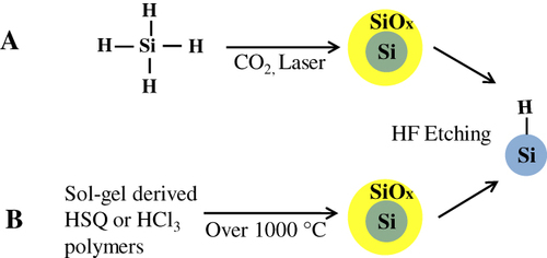
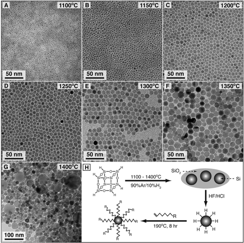
Thermolysis of silicon sub-oxide. Thermolysis of silicon sub-oxide is one of the routes to prepare SRO consisting of the silicon nanodomain in SiO2. To produce colloidally stable, free-standing silicon QDs, further etching and passivation were investigated by many groups. In earlier studies, silicon/silica core/shell nanostructures were reported to show visible emission. The starting precursor was a sol–gel-derived glass from triethoxysilane. After annealing under an argon atmosphere in the range of 1000–1200 °C, the product was composed of a silicon/silica mixture. As predicted, the product was not QDs, and was required by fluoride etching for libration [Citation97]. Liu et al used this technique to prepare silicon. Thermal annealing of commercially available SiOX (X = 0.4–1.8) in flowing argon at 900 °C was performed to obtain the silicon nanodomain embedded by silica glass. The product was then etched by HF to prepare fluorescent silicon. It was confirmed by HRTEM that the product etched with HF was silicon QDs of 4.2 nm diameter, and the polydispersity was estimated to be around 12%. The formation of a diamond cubic lattice was confirmed by XRD [Citation98]. The Veinot group did extensive studies on this process using different precursors. In 2006, Veinot and co-workers used commercial HSQ as a suitable molecular precursor to prepare a similar sol–gel glass upon reductive thermal heating in a 4% H2 containing inert atmosphere. Subsequent liberation of free-standing silicon QDs was done by HF etching. The emission from as-prepared Si QDs covered the visible spectrum depending on the size (see figure (B)). The size of QDs was controlled by the etching time and also by thermal decomposition temperature [Citation99]. Later, a similar sol–gel polymer was prepared from hydrolyzed HSiCl3 and used as an efficient cost-effective precursor for the formation of nanocrystalline silicon, embedded in a silica matrix. Since Pavesi's study in 2003, a series of thermolyses of the sol–gel-derived polymers to prepare a silicon/silica composite and further etching treatment to produce QDs becomes popular because of the many advantages including high chemical yield and good cost performance [Citation28, Citation29, Citation100–Citation103]. Moreover, PL spectral lines can be continuously tuned in the range from green to NIR wavelengths by rough control of HF etching time as shown in figure . By varying the thermolysis temperature, we can see the different relationship between etching time and emissions due to change in the size of nanocrystals, encapsulated in a silica matrix. As evidenced in figure , the difference in thermolysis temperature controls the size of the QDs.
Figure 4 PL spectra of pentane solutions of red-, orange-, yellow- and green-emitting silicon QDs. Inset: photographs of PL observed from each pentane suspension upon exposure to UV light (365 nm). Reprinted with permission from [Citation91]. ©2006, American Chemical Society.
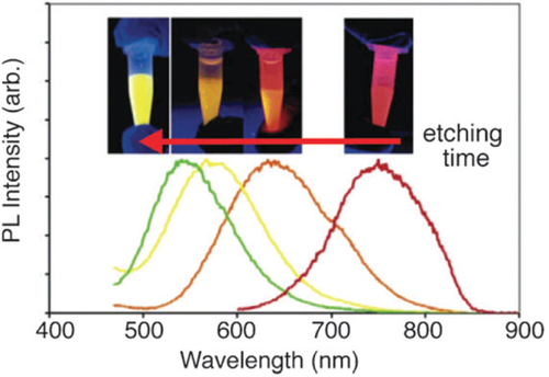
Figure 5 TEM images of alkene-passivated silicon nanocrystals generated by decomposition of hydrogen silsesquioxane (HSQ) at the indicated temperatures. (H) Synthetic pathway from HSQ to alkyl passivated silicon nanocrystals. Reprinted with permission from [Citation21]. ©2012, American Chemical Society.
In this subsection we compare various synthetic processes for preparing silicon QDs. Two approaches have been extensively studied. The bottom-up approach starts from molecular silicon as a starting material, and the top-down approach is performed by scale down of bulk crystalline silicon. All approaches have both advantages and disadvantages. Roughly, in the chemical solution phase reduction method, the advantages are (i) convenient for QDs preparation, (ii) chemically flexible and (iii) ease of access to a variety of surface chemistries. Possible disadvantages are (i) low chemical yield, (ii) much organic waste production and (iii) limited tuning property (narrow emission ranging from NUV to blue or aqua wavelengths). In the case of gas-phase condensation of the silicon precursor, the chemical yield is improved and full color of visible emissions is achieved. However, it needs extensive setup which is costly and also further passivation is needed to give a colloidal solubility which is not so flexible. Thermolysis of sol–gel-derived polymers followed by fluoride etching has many advantages including (i) gram-scale production, (ii) well-controlled emission wavelengths and (iii) cost effectiveness. However, we see several obstacles to further development. The most problematic phenomenon is instability of the emission, and this instability is independent of storage conditions including the atmosphere. Second, these methods require post-treatment with HF which is hazardous. As a common problem, nanocrystals immediately aggregate upon exposure to air due to hydride capping. Also the emission properties are affected by air. It is not so easy to unbind the aggregate into individual nanocrystals for re-dispersion in any solvents. Aggregation and air exposure make the surface passivation process inefficient, resulting in a lower coverage of surface monolayers compared to the chemical reduction method, which allows in situ surface modification with monolayers without exposure to air.
In the case of top-down approaches, we see several disadvantages including lower yield and broad size distribution. A unified simple approach to produce stable silicon QDs with a tunable emission spectrum covering the NUV to NIR range is needed.
Surface chemistry of Si QDs
Surface modification is one of the challenging and important subjects to improve the photophysical properties of semiconductor QDs including silicon. Unlike direct bandgap semiconductors, there are still many indeterminate points about the relationship between QD surface configuration and PL property. Wafer chemistry of silicon has been studied broadly and developed very well [Citation103–Citation111]; however, contrary to silicon wafers the surface structure of silicon QDs is inhomogeneous and much more complex. Owing to the large surface area-to-volume ratio, the bare surfaces of the QDs are highly sensitive to oxygen and water molecules. A number of theoretical and experimental studies have indicated that the surface properties of silicon QDs have a strong influence on both the bandgap and the radiative decay time. In this regard, surface chemistry is one of the important parameters that must be controlled if these materials are to be fully understood and to realize their potential applications. Surface modification of silicon QDs prevents undesired oxidation, and gives chemical durability and solubility to make a colloidal solution. In addition, modified QDs can be processed using the well-developed purification and fabrication techniques of organic chemistry [Citation112].
Surface passivation starts by preparing a hydrogenated or halogenated (Si–X; X = Cl, Br or I) silicon surface, and is performed by replacing the Si–X or Si–H bonds with organic monolayers through either one of the stable covalent carbon–silicon or oxygen–silicon linkages as illustrated in figure . In the early period of research on silicon QDs, there were no attempts to tailor QD surface chemistry. Many researchers confined their studies to using well-defined oxide shell covering core silicon [Citation66]. However, the lack of PL stability of porous silicon is a major barrier then to think of its commercial applications. Surface modification of porous silicon with functional groups was started as the initial step to stabilize PL property. In earlier studies, derivatization of porous silicon by Grignard reagents at room temperature was done by Kim and co-workers, where the porous silicon surface was functionalized with alkyl group reagents through interfacial carbon–silicon bonds [Citation113]. At that time, numerous studies on surface passivation were carried out [Citation114–Citation117]. One of the initial cases of Si QD surface passivation was performed by attaching a methoxy moiety on the surface. In this study, silicon QDs capped with chlorine atoms were prepared by reducing SiCl4 with KSi [Citation49]. Next, methanol was added to the solution with chloride-terminated QDs for methoxylation. Later, Stewart and co-workers applied white-light assisted reactions to hydrosilylation of 1-alkenes and 1-alkynes on silicon QDs [Citation118]. Further progress in surface modification was made by Yang et al. They reported a low-temperature solution synthesis of silicon QDs [Citation119]. The reaction with SiCl4 apparently produces a surface terminated with chlorine atoms, and the Si–Cl bonds were replaced by alkyl groups using alkyllithium or Grignard reagents to produce alkyl-capped QDs. They produced successfully methyl-, ethyl- and n-butyl-terminated QDs without surface oxide. Since this study in 1999, surface functionalization of silicon QDs has gained attention, leading to the development of various solution routes. Korgel and co-workers reported a novel method to prepare brightly luminescent, surface-passivated silicon QDs in supercritical organic solvents at high temperature and pressure. Diphenylsilane was decomposed at 400–500 °C and 80 bar pressure to crystallize silicon and then capping with octanethiol produced stable, protected and spherical well-crystallized silicon QDs [Citation30, Citation120]. As noted previously, CO2 laser-induced pyrolysis of silane-derived silicon QDs was further modified with different ligands by Li et al. 1-Octadecene and undecylenic acid were employed as ligands for surface modification via hydrosilylation [Citation89, Citation90]. FTIR spectra confirmed the covalent attachment of carbon atoms to the silicon surface. To achieve silanization, the silanol surface is generated by washing silicon QDs with 20% HNO3 or a mixture of concentrated sulfuric acid and hydrogen peroxide. Infrared study confirms the presence of siloxane monolayers [Citation121]. Conducting polymer-coated silicon QDs were also prepared on the silanol surface [Citation122].
Figure 6 Schematic illustrations of chemical routes for surface passivation of (A) halide-terminated and (B) hydrogen-terminated silicon QDs.
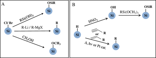
Photo-induced hydrosilylation was used to prepare hydrophobic and hydrophilic silicon QDs. In particular, water solubility is given by hydrosilylation by allyamine or acrylic acid on hydrogen-terminated silicon QDs. Li and Ruckenstein [Citation123] modified the hydride-terminated surface by the graft polymerization of acrylic acid under NUV irradiation. Hua et al improved the molecular coverage of surface monolayers by increasing the silicon–hydrogen density of the QD surface. In addition, they employed many compounds that each contained a terminal double bond such as 1-dodecene, 1-octadecene, 1-octene, 5-hexene-1-ol, undecanol, ethyl undecylenate, styrene and vinyl acetate for photo-initiated hydrosilylation [Citation124]. Other solution routes for surface chemistry were mostly in situ modifications. For example, the amine-capped QD surface was prepared from hydride reduction of SiCl4 with LiAlH4 in absolute toluene and subsequent hydrosilylation was done by allylamine in the presence of hexachloroplatinic acid as a catalyst [Citation74, Citation77]. A similar approach for hydrosilyation was followed in the case of hydride-capped QDs prepared via thermolysis of sol–gel-derived polymers. After liberation of hydrogen-terminated QDs by fluoride etching, a thermal radical reaction between 1-alkenes (or 1-alkynes) and hydrogenated QDs produces colloidal QDs [Citation28, Citation125, Citation126]. The key for tailoring the surface chemistry is the formation of chemically active surfaces including Si–Cl, Si–Br, Si–H and Si–OH bonds that allows subsequent derivatization. In reduction routes, halogen atoms bonded to the silicon surface are replaced in situ by alcohols, Grignard reagents or alkyl lithium. Due to the fact that the starting QDs are isolated without aggregation in the solvent, it is easy to modify each surface with the desired molecules without exposing to air; however, in those cases emission ranges are limited to the NUV–blue regions. Other routes except for in situ chemistry require a two-step process as follows. By HF or HF–HNO3 treatment, first a Si–H or Si–OH bond is formed and then that Si–H or Si–OH bond is replaced by Si–C or Si–O, respectively. In this treatment some trace of oxide in the surface is commonly unavoidable.
Photophysical properties
Due to the indirect bandgap nature of bulk crystalline silicon, it is not naturally capable of accomplishing efficient radiative recombination. Free electrons tend to exist in the X valley of the conduction band, which is not aligned with free holes in the valence band. Therefore, if electron–hole (e–h) carrier recombination has to lead to emission of a photon, a phonon must be involved in conserving the crystal momentum. Canham discovered in 1991 efficient light emission from porous silicon which was attributed to quantum confinement. Due to geometrical confinement in the nanoscale, uncertainty in k-space results in delocalization of carriers in k-space thus allowing zero phonon optical transitions and significantly enhancing the oscillator strength of the zero phonon transitions in small silicon nanocrystals.
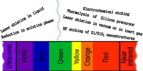
However, the story of carrier transition for recombination is not so simple. Due to the undeveloped method to synthesize QDs with continuous emission-tuning features in the whole of the NUV–VIS–NIR region the relationship between Si QDs and corresponding photophysical properties has not been systematically discussed. Silicon QDs are roughly classified in terms of PL features into two regions: one covers the NUV–aqua emission (λem = 300–500 nm) region and the other covers the green–NIR emission (λem = 500–950 nm) region, respectively. Interestingly, the tuning range of emissions strongly depends on the methods as shown in figure where we summarize the synthetic methods of silicon QDs and their corresponding emission zones. The long-wavelength visible and NIR PL spectra are commonly observed from the QDs synthesized by (i) laser ablation in gas (hydrogen or helium) or vacuum phase and (ii) thermolysis or pyrolysis of silicon precursors. On the other hand, silicon QDs emitting the lights in the NUV–blue range are synthesized by (iii) electron reduction of silicon halides or silane molecules in solution phases and (iv) laser ablation in a liquid. Besides, a blue light emission from the core/shell silicon/silica nanoparticles irrespective of the preparation method was also reported. Interestingly, PL decay behaviors are also very much different in these two emission regions indicating a fundamental difference in the PL mechanism. Decay lifetimes of the green–NIR-emitting QDs are in the microsecond level whereas those of the NUV–blue-emitting QDs are always in the nanosecond level [Citation140, Citation141]. In the next sub-section, we will highlight the emissions depending on the synthesis methods, and summarize the proposed decay mechanisms.
Figure 7 Emission range covered by silicon QDs synthesized by different methods.
Emissions in the green–NIR region
After Canham's discovery, PL spectra of colloidal silicon QD suspensions were reported in 1992. The PL maxima of the emissions varied between 750 and 650 nm for different solvent preparations, and the spectral line widths at half-maximum were typically 200 nm. The PL quantum yields (QYs) were not reported [Citation53]. Theoretical and experimental studies by Brus et al gave an opportunity to discuss the emission origin. Specifically, they provided size-dependent visible PL spectra to claim direct evidence of the quantum confinement effect. In that study, 3–8 nm silicon QDs were prepared by aerosol reaction and the silicon cores are encapsulated with 1.2 nm silicon oxide shells. The PL QYs were approximately 5% at 300 K; however, they increased to reach to 50% at low temperature. Both size-selective precipitation and size-exclusion chromatography were performed to discuss the possibility of size-dependent emission. The emission range varied between 600 and 900 nm, and depended on the size of the crystalline core of silicon. One significant observation was also made regarding the effect of surface passivation on emission properties. They observed that, due to oxide passivation, silicon QDs show bandgap shifts to red wavelengths, relatively high PL QYs, and low radiative rates. They measured the PL decay profile by fitting with a single exponential equation and calculated the 630 nm average lifetime increases from 50 μs at 293 K to about 2.5 ms at 20 K. These data were explained in the context of unimolecular decay of the e–h pair via two competing mechanisms, radiative Γr and non-radiative Γnr rates; then τ−1 = Γr + Γnr and QY = Γr/(Γr + Γnr). Below 50 K, the PL intensity is essentially constant while the lifetime continues to elongate. Therefore, the inference was made that radiative decay mechanisms dominated in low temperature decay and that the non-radiative part, which they proposed arose from the influence of imperfect crystallites with emission quenching defects, actually decreased PL QYs from 100%. From the broad absorbance near 3–4 eV it was suggested that the nanocrystallites have indirect bandgaps [Citation80, Citation82]. The authors also compared the optical properties of QDs of direct and indirect bandgap semiconductors to discuss the difference in transition. Unlike the QDs of direct bandgap semiconductors, silicon QDs had no discrete transition.
Li et al reported first the gram-scale synthesis of silicon QDs with emission-tunable features in the visible range. According to the report the emission maxima of PL spectra were controllable in the wavelength range from 800 to 500 nm, and this tuning was achieved by precisely controlling the synthesis conditions including HF etching time. Unfortunately, PL QYs were not enlightened in the paper [Citation89]. In earlier studies, PL QYs were estimated using the ensemble of silicon QDs because of the undeveloped size separation process, and were reported to be of the order of a few per cent [Citation73, Citation80]. Over the past few years there has been mounting evidence that further improvement of the optical properties can be achieved through careful passivation of the silicon QDs. A high PL QY (as high as 23%) was achieved by termination of the silicon surface with organic monolayers [Citation120]. Jurbergs et al [Citation95] reported silicon QDs with 60% PL QYs by plasma synthesis followed by surface passivation with organic ligands under strict exclusion of oxygen. The efforts on thermolysis of sol–gel-derived polymers from HSQ or HSiCl3 produced silicon QDs which allow tuning of PL in the emission range from 550 to 950 nm. PL QYs of the hydrogen-terminated silicon QDs were less than 10%, and most importantly they decay under ambient conditions. As expected, the PL QYs drastically increase up to 40–50% through surface passivation with optimum organic molecules or silica shells [Citation28, Citation99, Citation101].
The PL origin of silicon QDs is still under consideration, but the appearance of the quantum confinement effect was discussed to explain the tuning mechanism in the emission range between green and NIR [Citation29, Citation81, Citation127]. As summarized, silicon QDs, which are prepared from high-temperature processing including gas-phase methods and thermolysis of sol–gel silicon-derived polymers followed by fluoride etching, have been believed to show size-dependent emission based on the quantum confinement effect. This quantum-confined bandgap emission behavior was fitted to the predictions of the effective mass approximation (EMA), and exhibits long-lived excited state lifetimes at the microsecond level which is believed to be due to the indirect bandgap nature inherited even in nanostructures. Theoretical and experimental studies are in favor of the appearance of the quantum confinement model to explain the mechanism of green–NIR emission [Citation30]. Very recently Hessel et al [Citation29] used the PL peak energy as a measure of the exciton energy of the QDs and plotted it as a function of size determined by small-angle x-ray scattering. They compared the experimental relationship between size and emission maxima with calculation based on the EMA, and found quite a good match:
where d is the QD diameter, e is the electron charge, εr is the relative permittivity, and me and mh are the effective masses of the electron and the hole, respectively.
However, the story of luminescence origin does not end here. PL spectral tuning cannot only be discussed on the basis of the quantum confinement effect as in the case of QDs of direct bandgap semiconductors. There are many theoretical and experimental studies showing that the surface properties of QDs have a strong influence on both the bandgap and the radiative decay time [Citation88, Citation103, Citation128]. In the case of silicon, the surface of silicon is immediately oxidized. It is believed that oxidation generates oxygen-related surface/interface states inside the bandgap, leading to the slow optical transition of e–h carriers. There is also a report of changing emission due to different ligands. Different surface chemistries play a major role in determining different emissions [Citation127]. Godefroo et al [Citation33] investigated the PL origin of hydrogen-terminated silicon QDs based on the theory of the cyclotron resonance phenomenon. A nanostructure of the silicon/silica core/shell system was used as a control. The authors measured PL spectra in a strong magnetic field and found a small blueshift of red emission with the density of magnetic flux, resulting in the confined carriers in the hydrogen-terminated silicon to give a discrete energy level. Therefore, the red PL origin is discussed by the appearance of the quantum confinement effect. On the other hand, there is no shift of emission when silicon/silica core/shell nanoparticles were used as the specimen, implying that the PL was caused by the defect-related emission. Electron spin resonance measurements were performed to monitor the presence or the absence of (paramagnetic) defects in the silicon/silica core/shell nanostructure.
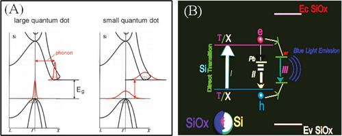
As summarized in the previous section, the available emission is limited to the range between 950 and 550 nm when using the methods focused on in this section [Citation28, Citation29, Citation129]. Tuning of the emission is attributed to the size-dependent bandgap of silicon owing to the quantum confinement effect. In addition, surface-related defect states also contribute to the emission tuning. A schematic diagram of the two mechanisms is shown in figure . According to the reports, nobody has observed silicon QDs showing PL spectra with emission maxima shorter than 560 nm even after prolonged HF etching for size reduction, e.g. over three nights. One possible reason might be a kind of ‘breakdown of the quantum confinement effect’. Importantly the breakdown of the quantum confinement effect is affected by both QDs size and surface state [Citation130]. A better understanding can be obtained by evaluating PL decay behaviors for different emissions. According to a study by Wu and co-workers, the average PL lifetimes decrease smoothly from 42 to 33 μs as the emission peak maxima change from 715 to 596 nm. The decrease in emission lifetime with the blueshift of the PL spectrum is simply explained by the quantum confinement model [Citation127]. Briefly, size reduction of QDs strengthens the quantum confinement effect, and gives the blueshift of absorption and emissions. The strengthened quantum confinement effect with reducing size increases the oscillator strength of radiative transitions of carriers, decreasing the radiative lifetime. On the other hand, surface-related states also play an important role in exciton recombination dynamics. There are several reports which have demonstrated a shift in the emission spectrum of silicon QDs due to surface functionalization. Interestingly, it was reported that the nature of the shift is dependent on the emission range of the silicon QDs [Citation31]. Red luminescent silicon QDs showed a blueshift in the emission spectrum to form orange luminescence after surface functionalization. In contrast, green luminescent QDs showed a redshift of emission to produce yellow-orange luminescence due to surface capping. This unpredictable phenomenon, i.e. green to yellow-orange, was explained as due to the shortened fundamental optical gap. Because of the replacement of hydrogen by the alkyl group on the silicon surface, leakage of the wave function occurs at the boundary between the QDs and the alkyl monolayer. In contrast, the mechanism of the PL spectral blueshift is still unclear. Not only hydrosilylation but also the oxide surface has a profound role in determining emission photon energy. The redshift of luminescence was observed when the green–yellow or green-emitting QDs were exposed to ambient air [Citation35]. In contrast, the red emission is blueshifted to orange under exposure to ambient air. The blueshift of luminescence is simply explained as a result of size reduction of core silicon with oxidation based on the quantum confinement effect. On the other hand, the redshift of PL spectra in ambient air could be explained by the surface-related states, suggesting that the surface-related defects should form the optical energy levels at lower positions than the conduction band minimum or at higher positions than the valence band maximum to shrink the fundamental energy gap. Such surface defect states do not affect the electronic structure if the core is relatively large. However, if the core is small enough to influence the electronic structure of a QD, the surface-related states might affect the confined structure to appear as inner energy states and then drastically change the PL behavior. The e–h carrier recombination mechanism was further investigated to explain this difference. Three e–h transition processes are discussed when the excited carriers relax down to the band-edges or optical trap states [Citation131]. Firstly, the band-to-band recombination is proposed. As the radiative center exists inside of the core silicon, light emission occurs as a result of e–h recombination across the gap. Photon energy of the emission corresponds to the magnitude of fundamental energy gaps reflecting the emission color. Therefore, the blueshift of the PL spectrum is caused by size reduction of the silicon core. The radiative lifetime is estimated to be of the order of microseconds for green–red-emitting QDs. Secondly, band-to-bound state recombination is proposed. There are many surface-related states near the conduction band and the valance band or in between which trap electrons or holes, respectively. These states are termed as surface-bound states. The radiative recombination occurs between one of the carriers (either an electron or a hole) in the surface-bound state, which is relaxed to surface states, and the opposite charge carrier (either a hole or an electron), which is inside the core. This recombination process is very fast, and the lifetime was calculated by Allan and co-workers to be about 1 ns [Citation128, Citation132, Citation133]. Thirdly, the bound-to-bound (i.e. surface-bound) recombination is proposed. Both electrons and holes which tunneled to the surface states recombined radiatively with surface-bound holes and surface-bound electrons, respectively. It is expected that this recombination is a slow process with a long response time because of the low coupling rate involved in tunneling or hopping processes. It is considered that the bound-to-bound recombination might become the dominant process in the silicon/silica core/shell nanostructure systems. These states are relatively insensitive to the silicon core size and are considered to behave either as radiative channels or as non-radiative traps. Unfortunately, the correlation between the surface-related states and the luminescent properties is not sufficiently well understood.
Figure 8 Schematic diagram of the possible mechanism of emission: (A) the quantum confinement model and (B) the oxide defect model. Reprinted with permission from [Citation28]. ©2011, American Chemical Society.
Emissions in the NUV–aqua region
Among all the emissions from silicon QDs, the blue emission is much more controversial and interesting despite the fact that the emission has been known since just after the discovery of silicon red emission. At present there are some reports in which the NUV–blue emissions are explained as a result of the radiative recombination of excitons in quantum confined silicon [Citation32]. An alternative origin is oxidation-induced defects at the silicon surface. Brus et al theoretically predicted in 2003 that ultrasmall (i.e. 1.1–1.4 nm) hydride surface-terminated silicon QDs are dominated by blue emission originating from a direct gap transition [Citation134, Citation135]. Experimentally, Li et al produced blue-emitting QDs by rapid thermal oxidization of orange-emitting particles [Citation89]. Kang et al [Citation136] executed some controlled oxidation of 3 nm silicon QDs and tuned the emission from red to blue. They confirmed that the blue emission originates from the silicon core because of stable and efficient blue emission even after etching in HF acid. Wolkin et al [Citation35] also observed the blue emission from porous silicon passivated with hydrogen atoms. A similar blue PL was obtained by Mizuno et al [Citation137] from photochemically etched porous silicon without oxide. Chen et al [Citation138] suggested that the silicon oxide layer is not responsible for the blue emission in porous silicon, as they observed a change in the peak position of the blue band upon varying the excitation wavelength. Much effort has been made to synthesize, through solution chemistry, oxide-free silicon QDs emitting blue light. Continuous tuning of the emission range from NUV to blue was achieved in 2010 for the first time, and the emission mechanism is proposed as a direct recombination of excitons confined in the nanocrystals. In that report silicon QDs were produced by reduction of SiCl4 that emit light within the NUV–blue range by precise size control of the nanocrystals and surface passivation with alkoxy monolayers. By changing the molar ratios of the starting SiCl4 and DMDOAB, QDs of different sizes were produced by continuous tuning of the PL spectra with emission maxima between 300 and 450 nm. These tuning features required accurate control of crystal size and complete surface passivation [Citation32].
In contrast to these observations, Zhu et al did not observe any change in the peak position of blue PL with increasing annealing temperature and therefore argued that blue PL originates from defect centers [Citation138, Citation139]. Kim et al [Citation140] also pointed out that the defects are responsible for blue emission in silicon. They observed that the oxidation of blue-emitting porous silicon does not cause any shift in their PL position. However, in contrast to the observation of Kim et al, Wolkin et al recorded a redshift in blue-emitting porous silicon after surface oxidation. Gupta and Wiggers [Citation34] observed the appearance of blue luminescence from the silicon QDs fabricated by re-oxidation of freshly etched particles. They investigated the effect of oxidation using freshly prepared red-emitting QDs, and claimed that the red emission is related to the quantum confinement effect, while the blue emission is related to the defect states at the newly formed silicon oxide surface. Recently, Yang et al reported the origin of the blue luminescent Si QDs. Figure (B) shows pictorially the mechanism. The silica shell forms near-interface traps (NIT) which are located at the interface areas between the core and the shell. Excitons first formed inside the quantum sized nanocrystals through direction transitions at the Γ or X point, and then some of them are caught by non-radiative Pb centers; the others transfer to and recombine at the NITs to emit blue light [Citation36]. Very recently, Dasog et al [Citation141] described a detailed comparison of silicon QDs obtained from three famous procedures. They also transformed red-emitting silicon QDs to blue-emitting QDs upon exposure to nitrogen-containing reagents. The blue PL that did not follow the EMA are prepared using solution methods at comparatively low temperatures (i.e. <400 °C). The reactions leading to the formation of silicon QDs typically involve direct reduction of silicon halides or the reaction of Zintl salts. Overview of the past blue emission mechanisms suggests that the PL origin might be different from the longer emission range of green–NIR. The difference in emission origin is obvious from the viewpoint of PL lifetime. NUV and blue PL relaxations are very fast at the nanosecond level whereas yellow, red and NIR PL relaxations are very slow at the microsecond level. Behind longer visible emission, both the quantum confinement effect and the surface effect have a role in emission properties and also the surface effect is size dependent. On the other hand, it is necessary to discuss the convinced nanostructure giving a blue PL feature because a core size of less than 1.5 nm is too small to have a diamond cubic lattice structure [Citation16].
Conclusions
In this review we have summarized the results of exciting recent breakthroughs on silicon QDs. First, silicon QDs prepared by various methods showed efficient emission and tunable optical properties with different surface functionalizations which is very much important for different applications. The size of the silicon core can be designed with angstrom-level precision and the surface of the core can be modified using a variety of organic chemistry techniques for desired applications and fundamental studies. A great deal of research is still essential in order to advance the field of luminescent silicon. While technical advances in synthesis procedures and reports of prototype devices that exploit the luminescence from silicon QDs and even stimulated emission have been in progress over the last decade, it is sensible to say that nanosilicon photonics is in its infancy. With high-quality materials of narrow size distribution and controlled surface chemistry in hand, it is reasonable to predict that unrealized photonic structures, including efficient LEDs, biomedical imaging, optical amplifiers, sensors, and possibly a silicon-based laser, will be realized in the near future. Studies reported to date indicate that these materials are extremely promising and therefore deserve continuous study.
References
- ZhaiTLiLMaYLiaoMWangXFangXYaoJBandoYGolbergD 2011 Chem. Soc. Rev. 40 2986 10.1039/c0cs00126k
- FaureBSalazar-AlvarezGAhniyazAVillaluengaIBerriozabalGMiguelYBergstromL 2013 Sci. Technol. Adv. Mater. 14 023001 10.1088/1468-6996/14/2/023001
- OsadaMSasakiT 2012 Adv. Mater. 24 210 10.1002/adma.201103241
- ArigaKJiQHillJ PBandoYAonoM 2012 NPG Asia Mater. 4 e17 10.1038/am.2012.30
- ArigaKVinuAYamauchiYJiQHillJ P 2012 Bull. Chem. Soc. Japan 85 1 32 1–32 10.1246/bcsj.20110162
- WinnikF MMaysingerD 2013 Acc. Chem. Res. 46 672 10.1021/ar3000585
- QianHZhuMWuZJinR 2012 Acc. Chem. Res. 45 1470 10.1021/ar200331z
- ShirasakiYSupranG JBawendiMBulovićV 2013 Nature Photon. 7 13 10.1038/nphoton.2012.328
- KramerI JSargentE H 2013 Chem. Rev. at press
- De FranceschiSKouwenhovenLSchönenbergerCWernsdorferW 2010 Nature Nanotechnol. 5 703 10.1038/nnano.2010.173
- DeySPalA J 2009 Appl. Phys. Lett. 94 082106 10.1063/1.3088861
- NagasakiY 2010 Sci. Technol. Adv. Mater. 11 054505 10.1088/1468-6996/11/5/054505
- YamasakiYAsamiHIsoshimaTKamiyaIHaraM 2003 Sci. Technol. Adv. Mater. 4 519 10.1016/j.stam.2003.12.008
- DeySPalA J 2013 RSC Adv. 3 13225 10.1039/c3ra41525b
- AcharyaSSarmaD DGolanYSenguptaSArigaK 2009 J. Am. Chem. Soc. 132 11282 10.1021/ja903539d
- ShirahataN 2011 Phys. Chem. Chem. Phys. 13 7284 10.1039/c0cp02647f
- GhoshBSakkaYShirahataN 2013 J. Mater. Chem. A 1 3747 10.1039/c3ta01246h
- PavesiLNegroL DMazzoleniCFranzoGPrioloF 2000 Nature 408 440 10.1038/35044012
- SugimotoHFujiiMImakitaKHayashiSAkamatsuK 2013 J. Phys. Chem. C 117 11850 10.1021/jp4027767
- GhoshBOgawaraMSakkaYShirahataN 2012 Chem. Lett. 41 1157 10.1246/cl.2012.1157
- KovalevDFujiiM 2005 Adv. Mater. 17 2531 10.1002/adma.200500328
- WangJ 1992 Phys. Rev. Lett. 69 3252 10.1103/PhysRevLett.69.3252
- GarridoB 2004 Nucl. Instrum. Methods Phys. Res. B 216 213 10.1016/j.nimb.2003.11.037
- NesbitL A 1985 Appl. Phys. Lett. 46 38 10.1063/1.95842
- VeinotJ G C 2006 Chem. Commun. 2006 4160 10.1039/b607476f
- FanJ YChuP K 2010 Small 6 2080 10.1002/smll.201000543
- MastronardiM LHendersonE JPuzzoD POzinG A 2012 Adv. Mater. 24 5890 10.1002/adma.201202846
- HendersonE JShuhendlerA JPrasadPBaumannVMaier-FlaigFFaulknerD O 2011 Small 7 2507
- HesselC M 2012 Chem. Mater. 24 393 10.1021/cm2032866
- EnglishD SPellL EYuZ HBarbaraP FKorgelB A 2002 Nano Lett. 2 681 10.1021/nl025538c
- GuptaASwihartM TWiggersH 2009 Adv. Funct. Mater. 19 696 10.1002/adfm.200801548
- ShirahataNTsuruokaTHasegawaTSakkaY 2010 Small 6 915 10.1002/smll.200902236
- GodefrooSHayneMJivanescuMStesmansAZachariasMLebedevO I 2008 Nature Nanotechnol. 3 174 10.1038/nnano.2008.7
- GuptaAWiggersH 2011 Nanotechnology 22 5 10.1088/0957-4484/22/5/055707
- WolkinM VJorneJFauchetP MAllanGDelerueC 1999 Phys. Rev. Lett. 82 197 10.1103/PhysRevLett.82.197
- YangS KLiW ZCaoB QZengH BCaiW P 2011 J. Phys. Chem. C 115 21056 10.1021/jp2075836
- RuizendaalLBhattacharjeeSPournazariKRosso-VasicMde HaanL H JAlinkG M 2009 Nanotoxicology 3 339 10.3109/17435390903288896
- SvrcekVSasakiTShimizuYKoshizakiN 2008 J. Appl. Phys. 103 023101 10.1063/1.2830798
- OkadaRIijimaS 1991 Appl. Phys. Lett. 58 1662 10.1063/1.105129
- WerwaESeraphinA AChiuL AZhouC XKolenbranderK D 1994 Appl. Phys. Lett. 64 1821 10.1063/1.111766
- UmezuIShibataKYamaguchiSSugimuraAYamadaYYoshidaT 1998 J. Appl. Phys. 84 6448 10.1063/1.368971
- MakinoTInadaMYoshidaKUmezuISugimuraA 2004 Appl. Phys. A: Mater. Sci. Process 79 1391
- MakinoTInadaMUmezuISugimuraA 2005 J. Phys. D: Appl. Phys. 38 3507 10.1088/0022-3727/38/18/028
- YamadaYOriiTUmezuITakeyamaSYoshidaT 1996 Japan. J. Appl. Phys. 35 (Pt 1) 1361 10.1143/JJAP.35.1361
- MakimuraTKuniiYMurakamiK 1996 Japan. J Appl. Phys. 35 (Pt 1) 4780 10.1143/JJAP.35.4780
- OriiTHirasawaMSetoT 2003 Appl. Phys. Lett. 83 3395 10.1063/1.1621457
- UmezuI MSenooH 2007 J. Phys.: Conf. Ser. 59 392 10.1088/1742-6596/59/1/083
- ShirahataN 2009 Chem. Commun. 2009 4684 10.1039/b905777c
- ShirahataNHirakawaDMasudaYSakkaY 2013 Langmuir 29 7401 10.1021/la303482s
- CanhamL T 1990 Appl. Phys. Lett. 57 1046 10.1063/1.103561
- CullisA GCanhamL TCalcottP D J 1997 J. Appl. Phys. 82 909 10.1063/1.366536
- CullisA GCanhamL T 1991 Nature 353 335 10.1038/353335a0
- HeinrichJ LCurtisC LCredoG MKavanaghK LSailorM J 1992 Science 255 66 10.1126/science.255.5040.66
- BleyR AKauzlarichS MDavisJ ELeeH W H 1996 Chem. Mater. 8 1881 10.1021/cm950608k
- HeathJ R 1992 Science 258 1131 10.1126/science.258.5085.1131
- DhasN ARajC PGedankenA 1998 Chem. Mater. 10 3278 10.1021/cm980408j
- BleyR AKauzlarichS M 1996 J. Am. Chem. Soc. 118 12461 10.1021/ja962787s
- MayeriDPhillipsB LAugustineM PKauzlarichS M 2001 Chem. Mater. 13 765 10.1021/cm000418w
- ZouJSanellePPettigrewK AKauzlarichS M 2006 J. Cluster Sci. 17 565 10.1007/s10876-006-0082-9
- BaldwinR KPettigrewK AGarnoJ CPowerP PLiuG YKauzlarichS M 2002 J. Am. Chem. Soc. 124 1150 10.1021/ja017170b
- ShirahataNFurumiSSakkaY 2009 J. Cryst. Growth 311 634 10.1016/j.jcrysgro.2008.09.084
- ShirahataNNakanishiTFurumiSSakkaY 2006 J Nanosci. Nanotechnol. 6 1823 10.1166/jnn.2006.209
- BalciM HMariaJVullum-BruerFLindgrenMGrandeTEinarsrudM A 2012 J. Cluster Sci. 23 421 10.1007/s10876-012-0448-0
- BaldwinR KPettigrewK ARataiEAugustineM PKauzlarichS M 2002 Chem. Commun. 2002 1822 10.1039/b205301b
- YangC SKauzlarichS MWangY CLeeH W H 2000 J. Cluster Sci. 11 423 10.1023/A:1009099416195
- NeinerDChiuH WKauzlarichS M 2006 J. Am. Chem. Soc. 128 11016 10.1021/ja064177q
- ZouJKauzlarichS M 2008 J. Cluster Sci. 19 341 10.1007/s10876-008-0182-9
- LiuQKauzlarichS M 2002 Mater. Sci. Eng. B 96 72 10.1016/S0921-5107(02)00293-3
- PettigrewK ALiuQPowerP PKauzlarichS M 2003 Chem. Mater. 15 4005 10.1021/cm034403k
- AtkinsT MLouieA YKauzlarichS M 2012 Nanotechnology 23 9 10.1088/0957-4484/23/29/294006
- AtkinsT MThibertALarsenD SDeySBrowningN DKauzlarichS M 2011 J. Am. Chem. Soc. 133 20664 10.1021/ja207344u
- WilcoxonJ PSamaraG A 1999 Appl. Phys. Lett. 74 3164 10.1063/1.124096
- WilcoxonJ PSamaraG AProvencioP N 1999 Phys. Rev. B 60 2704 10.1103/PhysRevB.60.2704
- TilleyR DWarnerJ HYamamotoKMatsuiIFujimoriH 2005 Chem. Commun. 2005 1833 10.1039/B4160695
- WarnerJ HHoshinoAYamamotoKTilleyR D 2005 Angew. Chem. Int. Edn Engl. 44 4550 10.1002/anie.200501256
- WarnerJ HRubinsztein-DunlopHTilleyR D 2005 J. Phys. Chem. B 109 19064 10.1021/jp054565z
- TilleyR DYamamotoK 2006 Adv. Mater. 18 2053 10.1002/adma.200600118
- LeeSChoW JKimY DKimE KParkJ G 2005 Japan. J. Appl. Phys. 44 (Pt 1) 5843 10.1143/JJAP.44.5843
- MurthyTMiyamotoNShimboMNishizawaJ 1976 J. Crystallogr. Growth 33 1 10.1016/0022-0248(76)90072-5
- LittauK ASzajowskiP JMullerA JKortanA RBrusL E 1993 J. Phys. Chem. 97 1224 10.1021/j100108a019
- WilsonW LSzajowskiP FBrusL E 1993 Science 262 1242 10.1126/science.262.5137.1242
- BrusL 1994 J. Phys. Chem. 98 3575 10.1021/j100065a007
- CannonW RDanforthS CFlintJ HHaggertyJ SMarraR A 1982 J. Am. Ceram. Soc. 65 324 10.1111/j.1151-2916.1982.tb10464.x
- FlintJ HDanforthS CCannonW RHaggertyJ S 1979 IEEE J. Quantum Electron. 15 D1 10.1109/JQE.1979.1069891
- CannonW RDanforthS CFlintJ HLaiK SHaggertyJ S 1979 Am. Ceram. Soc. Bull. 58 337
- LedouxG 2000 Phys. Rev. B 62 15942 10.1103/PhysRevB.62.15942
- LedouxGGongJHuiskenFGuilloisOReynaudC 2002 Appl. Phys. Lett. 80 4834 10.1063/1.1485302
- LedouxGGongJHuiskenF 2001 Appl. Phys. Lett. 79 4028 10.1063/1.1426273
- LiX GHeY QTalukdarS SSwihartM T 2003 Langmuir 19 8490 10.1021/la034487b
- LiX GHeY QSwihartM T 2004 Langmuir 20 4720 10.1021/la036219j
- LiXHeS STalukdarS SSwihartM T 2004 Phase Transit. 77 131 10.1080/01411590310001623283
- DongYBapatAHilchieSKortshagenUCampbellS A 2004 J. Vac. Sci. Technol. B 22 1923 10.1116/1.1771667
- BapatAPerreyC RCampbellS ACarterC BKortshagenU 2003 J. Appl. Phys. 94 1969 10.1063/1.1586957
- MangoliniLThimsenEKortshagenU 2005 Nano Lett. 5 655 10.1021/nl050066y
- JurbergsDRogojinaEMangoliniLKortshagenU 2006 Appl. Phys. Lett. 88 3
- PiX D 2008 Nanotechnology 19 5
- SoraruG DModenaSBettottiPDasGMariottoGPavesiL 2003 Appl. Phys. Lett. 83 749 10.1063/1.1587876
- LiuS MYangYSatoSKimuraK 2006 Chem. Mater. 18 637 10.1021/cm0519636
- HesselC MHendersonE JVeinotJ G C 2006 Chem. Mater. 18 6139 10.1021/cm0602803
- KellyJ AHendersonE JVeinotJ G C 2010 Chem. Commun. 46 8704 10.1039/c0cc02609c
- HendersonE JKellyJ AVeinotJ G C 2009 Chem. Mater. 21 5426 10.1021/cm902028q
- KellyJ AShukaliakA MFleischauerM DVeinotJ G C 2011 J. Am. Chem. Soc. 133 9564 10.1021/ja2025189
- NunezJ R RKellyJ AHendersonE JVeinotJ G C 2012 Chem. Mater. 24 346 10.1021/cm203085f
- GuptaVMadaanNJensenD SKunzlerS CLinfordM R 2013 Langmuir 29 3604 10.1021/la304491x
- BlakeR BPeiLYangLLeeM VConleyH JDavisR CShirahataNLinfordM R 2008 Macromol. Rapid Commun. 29 638 10.1002/marc.200700752
- RijksenBvan LagenBZuilhofH 2011 J. Am. Chem. Soc. 133 4998 10.1021/ja110844e
- ShirahataNNakanishiJEchikawaYHozumiAMasudaYItoSSakkaY 2008 Adv. Funct. Mater. 18 3049 10.1002/adfm.200800438
- GalopinEPiretGSzuneritsSLequetteYFailleCBoukherroubR 2010 Langmuir 26 3479 10.1021/la9030377
- ScheresLGiesbersMZuilhofH 2010 Langmuir 26 4790 10.1021/la9035503
- YangL 2009 Langmuir 25 5674 10.1021/la804272n
- ShirahataNYonezawaTMasudaYKoumotoK 2004 Langmuir 20 1517 10.1021/la035179g
- ShirahataNHirakawaDSakkaY 2010 Green Chem. 12 2139 10.1039/c0gc00502a
- KimN YLaibinisP E 1998 J. Am. Chem. Soc. 120 4516 10.1021/ja9712231
- BatemanJ EEaglingR DWorrallD RHorrocksB RHoultonA 1998 Angew. Chem. Int. Edn Engl. 37 2683 10.1002/(SICI)1521-3773(19981016)37:19%3C2683::AID-ANIE2683%3E3.0.CO;2-Y
- SievalA BVleemingVZuilhofHSudholterE J R 1999 Langmuir 15 8288 10.1021/la9904962
- WaynerD D MWolkowR A 2002 J. Chem. Soc.-Perkin Trans. 2 23
- ShirahataNHozumiAYonezawaT 2005 Chem. Rec. 5 145 10.1002/tcr.20041
- StewartM PBuriakJ M 2001 J. Am. Chem. Soc. 123 7821 10.1021/ja011116d
- YangC SBleyR AKauzlarichS MLeeH W HDelgadoG R 1999 J. Am. Chem. Soc. 121 5191 10.1021/ja9828509
- HolmesJ DZieglerK JDotyR CPellL EJohnstonK PKorgelB A 2001 J. Am. Chem. Soc. 123 3743 10.1021/ja002956f
- TuC CZhangQ FLinL YCaoG Z 2012 Opt. Express 20 A69 10.1364/OE.20.000A69
- LiZ FSwihartM TRuckensteinE 2004 Langmuir 20 1963 10.1021/la0358926
- LiZ FRuckensteinE 2004 Nano Lett. 4 1463 10.1021/nl0492436
- HuaF JErogbogboFSwihartM TRuckensteinE 2006 Langmuir 22 4363 10.1021/la0529106
- KellyJ AVeinotJ G C 2010 ACS Nano 4 4645 10.1021/nn101022b
- MastronardiM L 2012 Small 8 3647 10.1002/smll.201201242
- YuWXuY MLiH MZhanX ZLuW B 2013 Appl. Phys. A 111 501 10.1007/s00339-013-7556-z
- LannooMDelerueCAllanG 1996 J. Lumin. 70 170 10.1016/0022-2313(96)00053-1
- MastronardiM L 2011 J. Am. Chem. Soc. 133 11928 10.1021/ja204865t
- MartinJCichosFHuiskenFvon BorczyskowskiC 2008 Nano Lett. 8 656 10.1021/nl0731163
- KochFPetrovakochVMuschikT 1993 J. Lumin. 57 271 10.1016/0022-2313(93)90145-D
- AllanGDelerueCLannooM 1996 Phys. Rev. Lett. 76 2961 10.1103/PhysRevLett.76.2961
- DelerueCLannooMAllanG 1996 Phys. Rev. Lett. 76 3038 10.1103/PhysRevLett.76.3038
- ZhouZ YBrusLFriesnerR 2003 Nano Lett. 3 163 10.1021/nl025890q
- ZhouZ YBrusLFriesnerR A 2003 Abstr. Pap. Am. Chem. Soc. 226 U440
- KangZ H 2009 Adv. Mater. 21 661 10.1002/adma.200801642
- MizunoHKoyamaHKoshidaN 1996 Appl. Phys. Lett. 69 3779 10.1063/1.116996
- ChenQ WLiX JJiaY BZhuJ SZhangY H 1997 J. Phys.: Condens. Matter 9 L151 10.1088/0953-8984/9/10/002
- ZhuMChenGChenP 1997 Appl. Phys. A 65 195 10.1007/s003390050565
- KimY SSuhK YYoonHLeeH H 2002 J. Electrochem. Soc. 149 C50 10.1149/1.1424287
- DasogM 2013 ACS Nano 7 2676 10.1021/nn4000644