
Abstract
Anodization techniques by alternating current (ac) are introduced in this review. By using ac anodization, laminated alumina films are fabricated. Different types of alumina films consisting of 50–200 nm layers were obtained by varying both the ac power supply and the electrolyte. The total film thickness increased with an increase in the total charge transferred. The thickness of the individual layers increased with the ac voltage; however, the anodization time had little effect on the film thickness. The laminated alumina films resembled the nacre structure of shells, and the different morphologies exhibited by bivalves and spiral shells could be replicated by controlling the rate of increase of the applied potentials.
Introduction
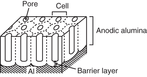
Anodic aluminum oxide (AAO) films with vertically oriented cylindrical pores are usually fabricated by the electric field-assisted oxidation of aluminum (Al) in acidic electrolytes [Citation1, Citation2]. The schematic model shown in figure illustrates the arrangement of single-pore-containing units known as cells, called porous anodic alumina (PAA). The sizes and spacing of the pores in the films can be controlled with nanoscale precision by varying the anodization parameters, resulting in very deep nanopores with high aspect ratios. The pores were formed naturally as ordered hexagonal cells as shown in figure under appropriate conditions [Citation2–Citation7].
Figure 1 Schematic model of an anodic alumina layer on an aluminum sheet.
PAA films have been used as templates or host materials in the fabrication of various nanostructures such as nanowires/rods [Citation8–Citation26], nanotubes [Citation27–Citation46] and nanoporous films [Citation47–Citation56]. These products have been utilized in a variety of promising applications such as magnetic recording media [Citation9–Citation16, Citation33, Citation34], thermoelectric materials [Citation17, Citation18], optical materials [Citation20–Citation22, Citation48, Citation49], sensors [Citation23–Citation25, Citation35], energy storage [Citation25, Citation26, Citation36, Citation37, Citation50], photocatalysis [Citation27, Citation51, Citation52], photovoltaic devices [Citation28, Citation29] and biomaterials [Citation53–Citation56].
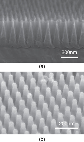
For applications of nanomaterials prepared from PAA, it is important to control the arrangement and morphology of the pores. The pore size of PAA is known to be controlled by pore widening treatment, where the pores are subjected to chemical etching, resulting in pores with various sizes. By using repeated anodization coupled with a pore widening treatment, tapered holes could be obtained as shown in figure (a) [Citation57–Citation60]. The tapered holes are useful to modify the polymer surface by filling the polymers, which are applicable for anti-reflection [Citation57], and can form metal nanocones by metal plating techniques as shown in figure (b) [Citation58–Citation60].
Figure 2 Cross-sectional SEM images of (a) hexagonal ordered PAA film with tapered holes, and (b) Ni film with corn structures prepared by electrodeposition from PAA film shown in (a).
Some researchers have developed pores with complex three-dimensional (3D) morphologies. Krishnan and Thompson [Citation61] reported a 3D nanoporous alumina structure with stepped pore diameters increasing from 55 to 85 nm or decreasing from 85 to 55 nm through a two-step anodization, assisted by an interface lithography process. Ho et al [Citation62] fabricated a multi-tiered branched PAA film consisting of an array of big pores branching into two to four smaller pores in succeeding tiers, which was realized by sequentially stepping down the anodization potential while etching of the barrier layer is performed after each step. Recently, several groups reported the fabrication of 3D PAA films with shaped pore geometries in periodically changed pore diameters through methods called ‘cyclic anodization’ by Losic et al [Citation63, Citation64], and ‘pulsed anodization’ and ‘oscillated anodization’ by Lee et al [Citation65, Citation66] in which pulsed or oscillated current signals, instead of constant current as in conventional anodization, were applied to the Al substrates program-controllably or spontaneously. More recently, Meng and co-workers [Citation67, Citation68] and Zaraska et al [Citation69] attempted to produce hierarchical PAA films with root-like pore channels by reducing the anodizing voltage in a factor of ratio (n = 2, 3) to increase the pore cell numbers. Katsuta et al [Citation70] demonstrated that 3D nanostructured porous alumina film, which consisted of two layers with cell diameter sizes of 340 nm φ and 640 nm φ (figure ), on a glass substrate exhibiting an angle-insensitive optical transmission property.
Figure 3 Cross-sectional SEM image of 3D nanostrucutred alumina film on a glass substrate, which consists of two-layers with cell sizes of 340 nm φ (upper) and 640 nm φ (lower). Reproduced with permission of [Citation70] (© 2007 Elsevier).

Wada et al [Citation71] reported the preparation of films with a laminated structure via the application of a high ac voltage. Most studies on the fabrication of AAO films have focused on direct current (dc) methods, with alternating current (ac) methods receiving scant attention. In particular, few reports concern ac anodization, and most of them describe the formation of thick films in which the pores were not hexagonal, in contrast to dc films [Citation72, Citation73]. Graeve et al [Citation74] recently reported the fabrication of ac AAO films that had a porous structure similar to that of films with pores prepared by short dc treatments. There are no reports about the formation of laminated structures as shown by Wada et al [Citation71], thus we focus on the laminated structure prepared by ac anodization in this review.
Ac anodization
Metal surfaces are exposed to both anodic and cathodic reactions during ac electrochemical processes, which include ac electrodeposition, ac electrochemical etching such as machining [Citation75] and ac electrograining [Citation76–Citation84] and ac anodization [Citation71–Citation74, Citation85, Citation86]. Electrodeposition is widely used to insert metals in pores such as PAA prepared by dc anodization as mentioned above. Both ac and dc electrodeposition have been used; however, it is easier to control the growth of the metal with ac than with dc. In ac electrochemical etching, surfaces are etched by anode and cathode reactions. In particular, ac machining can form very fine tips for scanning tunneling microscopy by the etching process. In this process, the generation of hydrogen gas was essential to machine very fine tips, because the gas formed bubbles around the metal wire which moved upward along the metal surface. In electrograining, a pitted morphology can be formed on an aluminum surface, which is required for low-voltage electrolytic capacitors [Citation76–Citation84, Citation87–Citation91].
In ac anodization, protective metal oxide layers are fabricated. For all ac processes, the metals are known to be dissolved by etching during the anodic half-cycle. Metal dissolution can also be accomplished by simple dc; however, the difference between ac and dc dissolution processes is the reduction of solution species (typically H+ to H2) during the cathodic half-cycle. The evolution of hydrogen gas distinguishes ac processes from dc processes.
The role of the cathodic half-cycle in the ac etch process has been explained in terms of (i) the formation of a precipitated aluminum oxyhydrate ‘etch film’ due to the increase in the local pH during the cathodic half-cycle [Citation76, Citation91]; (ii) the hydration of the surface oxide film [Citation92–Citation94]; or (iii) the mechanical deterioration of the surface oxide film due to hydrogen gas generation [Citation95–Citation97]. In ac electrograining, Dyer and Alwitt [Citation91] proposed a pit-on-pit propagation mode. Cubic etch pits, newly formed during the anodic half-cycle, are covered with the etch film, which is formed during the following cathodic half-cycle. The next pit is initiated during the next anodic half cycle at a weak point in the etch film at the pit base, and grows by undercutting the pre-existing etch film until a new etch film is formed in the next cathodic half-cycle. Recently, Ono and Habazaki [Citation98] investigated the role of the cathodic half-cycle by measurement of electrostatic capacitance as an etch factor. The amount of the etch film (i.e. the sum of aluminum oxyhydroxide and aluminum oxide) was related to the etch factor independently of the wave functions. However, it was found that the cathodic half-cycle was not a crucial factor in the development of an etched layer. Hammons et al investigated the transport of formed H2 gas [Citation99] through Al(OH)3 gels formed on an Al surface [Citation100]. It was found that gas permeation occurred through collapsible pores, and affected the pit morphology.
The morphology resulting from ac anodization has been investigated, and the surfaces were found to have small pores and cells [Citation73, Citation74, Citation85]. The structures were similar to those prepared by dc anodization at the early stage [Citation74]; however, those shapes were not retained after extended or high-voltage anodization [Citation73]. The composition of the film prepared in sulfuric acid was estimated and the sulfur content was not related to the anodizing conditions [Citation85, Citation101]. The effects of current density or potential and electrolyte temperature and concentration on film growth were also investigated [Citation102]. The thickness of the films increased as the reaction time increased [Citation72, Citation86], but the hardness decreased with the anodization time because the porosity increased [Citation86]. Kape [Citation72] reported that the thickness of anodic films prepared by the ac process could exceed 1 μm depending on the anodization time. However, the morphologies of thick films prepared by ac have not been well characterized. Wada et al [Citation71] investigated thick films prepared by ac anodization and reported the formation of laminated layer structures similar to that of shell nacre, but further investigations have not been performed. The morphological effects of anodization conditions such as the electrolyte identity and applied voltage have not been investigated.
Formation of laminated alumina films
Recently, Segawa et al [Citation103, Citation104] investigated the formation of laminated films by ac anodization. For the preparation, high-purity aluminum sheets (99.99%, 10 mm × 40 mm × 1 mm, Wako Pure Chemical Industry, Ltd, Osaka, Japan) were used as samples. Anodization was performed using electrolyte solutions of sulfuric acid (> 96%), oxalic acid (H2C2O4·2H2O, >99.5%), phosphoric acid (> 85%) or citric acid (C6H8O7·H2O, >99.5%), purchased from Kanto Chemical Co., Inc., Tokyo, Japan. To understand the influence of pH on the formation of the laminate structure, the concentration of the electrolyte solution was varied from 0.0375 to 0.3 mol l−1. For all other purposes, the concentration of the electrolyte solution was fixed at 0.3 mol l−1. A powerful cooling system (Cool-Line, CLH300, Yamato Scientific Co., Ltd, Tokyo, Japan) and a large electrolysis cell (1 l) were employed to maintain the solutions at 12 °C. A platinum sheet was used as the counter-electrode. All anodization trials were conducted by applying a dc voltage of 25 V for 20 s, to avoid exfoliation and errors due to dielectric breakdown. The ac power was subsequently applied and the ac voltage (V) was raised at a rate of 2 V s−1, and that voltage was maintained thereafter. The time elapsed between turning on the dc supply and turning off the ac supply was considered to be the anodization time (t). The waveform of the ac power was typically a sine wave with a frequency of 50 Hz. The ac voltage, V, represents the effective voltage of the sine wave, and the voltage applied √ 2V at the maximum. Both ac and dc power were generated by a power supply (Kikusui Electronics Corp., Yokohama, Japan, PCR500M 270 V/2.5 A) that was connected to a computer to control variations in voltage and current during the anodization.
Figure shows scanning electron microscopy (SEM) cross-sectional images of alumina films prepared by ac anodization for 300 s in (a) oxalic acid at 50 V, (b) phosphoric acid at 100 V, (c) sulfuric acid at 50 V and (d) citric acid at 200 V. The applied voltage was varied depending on the electrolyte [Citation105], but the concentration of each acid solution was 0.3 mol l−1. The images in figures (a-1), (b-1), (c) and (d) are expansions to more clearly visualize the layer structures. Whole films of figures (a-1) and (b-1) are shown in figures (a-2) and (b-2), respectively. Laminated films were formed parallel to the underlying aluminum sheet and remained adhered to the sheet after the completion of the anodization process. Although the SEM images of the whole films appeared to show the alumina film layers peeling from the aluminum sheet, this was due to SEM sample preparation. In each laminated layer, the top surface depended on the electrolyte, but the bottom surface had small wave-like structures which were similar to those of the barrier layers noticed in the films prepared by dc anodization. The structures of the samples laminated in sulfuric acid and oxalic acid were similar in appearance, with layers stacked in close proximity. Each layer was composed of a surface portion that exhibited numerous pores (more appropriately called pre-pores) with diameters of approximately 8 nm in sulfuric acid and 9 nm in oxalic acid, and a lower solid portion with no pores. In the case of samples treated in phosphoric acid, the bulk film was composed of two distinguishable regions: one was smooth and the other was rough, and the spacing between the layers was greater than the others (figure (b-1)). As seen in figure (b-2), these layers were not homogeneous, but rather, consisted of rough segments with numerous pores approximately 12 nm in diameter. This morphology was similar to the interface between the pores and oxides formed by dc anodization [Citation106]. Considering the difference in the thickness between the rough and smooth segments, the latter appeared to have been formed by the disappearance of pores. It was not possible to confirm that laminated layers were formed in the case of samples processed in citric acid solution for 300 s between 120 and 210 V. From the images of the whole films, the total number of layers in the film did not correspond to the number of anodic half-cycles, which occurred at 50 cycles s−1. This means that film formation did not occur in each of the anodic half-cycles, but rather, after repeated reaction.
Figure 4 Cross-sectional SEM images of the laminated alumina films prepared for 300 s and at 40 V in (a) oxalic acid, (b) phosphoric acid, (c) sulfuric acid and (d) citric acid. Panels (a-2) and (b-2) are images of whole films of (a-1) and (b-1).
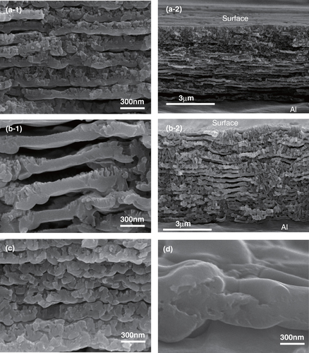
Figure shows plots of the average thicknesses of the all the layers versus different ac voltages over an anodization time of 300 s. The layer thicknesses increased linearly with the ac voltage. The thickness of the film prepared using phosphoric acid was lower than those of the other films, and the slope of its curve was 0.85, and similarly reduced. The films prepared using sulfuric and oxalic acids were very similar in thickness (within experimental error) and were not affected by the electrolyte concentrations. The slopes of the curves for these films were also similar and ranged from 1.59 to 1.86, with an average of 1.68. As mentioned above, the bottom surfaces of the layers were similar to those of the barrier layers observed in films prepared by dc anodization; however, the top surfaces of the layers had pre-pores, as could be seen from their SEM images. The thicknesses of the layers were measured by considering both the pre-pore-free and pre-pore-containing segments, for the films prepared using sulfuric and oxalic acids. This was because every layer had pre-pore-free and pre-pore-containing segments and it was difficult to measure the thicknesses of the segments that contained pre-pores. However, in the case of the film prepared using phosphoric acid, only the thickness of the barrier layer was measured. Thus, the thickness of the film fabricated using phosphoric acid was lower than those of the others. In a previous study on dc anodization, the anodization rate of the barrier layer was found to be about 1.3 nm V−1 [Citation107]. If each layer of the ac-anodized films is assumed to be composed of a layer similar to the barrier layer of the dc-treated samples, the slope of the anodization rate would be . This is because the ac voltage used in this paper represents the effective voltage, and the maximum voltage is
times larger. As can be seen from this figure, the average of the slopes, 1.68, was close to 1.3
. However, in the case of the film fabricated using phosphoric acid, the slope was smaller than
. This suggests that the barrier layer was dissolved in the acid as well as the porous segments with the pre-pores, resulting in the reduced thickness compared to the other films. That the slope of the film fabricated using phosphoric acid was small implied that the dissolution rate of the porous segment and the barrier layer increased with an increase in the anodization voltage. It was found that the dissolution of the pre-pore-containing segments affected the thickness of the layer.
Figure 5 Thickness of the individual layers versus the ac voltage for an anodization time of 300 s. •: 0.3 mol l−1 and ◊: 0.15 mol l−1 sulfuric acid; •: 0.3 mol l−1 and ◊: 0.5 mol l−1 oxalic acid; and •: 0.3 mol l−1 phosphoric acid.

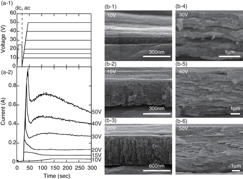
Figure (a) shows the relationships between (a-1) the applied voltage and time and (a-2) the current produced with time for different applied voltages. The curves correspond to a film anodized for 300 s in 0.3 mol l−1 oxalic acid. Figure (b) shows cross-sectional SEM images of the films produced upon the application of ac voltages of (b-1) 10 V, (b-2) 15 V, (b-3) 20 V, (b-4) 30 V, (b-5) 40 V and (b-6) 50 V. For all the applied voltages except 10 V, the current increased drastically at 25 s after the start of the ac treatment, reached a maximum value, and then decreased. Further, the maximum current increased and the rate at which the current decreased from its maximum value also was reduced with an increase in the applied voltage. In the case of applied voltages of 15 and 20 V, after decreasing, the currents leveled off. For applied voltages of 30, 40 and 50 V, the current increased gradually again before finally decreasing gradually. For the 10 V applied voltage, the current increased gradually for approximately 140 s and then leveled. Overall, the current increased with an increase in the applied voltage. This demonstrated that high anodization voltages induced high anodization currents, resulting in increased charge transfer during the anodization process. As can be seen from figure (b), the structures of the synthesized films depended on the voltage applied. Films consisting of laminated layers were obtained at voltages greater than 30 V. The films prepared at 10, 15 and 20 V were porous and did not have laminated structures. The thicknesses of the films increased with an increase in the applied voltage. In particular, the film prepared at 20 V contained vertical pores and had a structure similar to that reported previously for films prepared by ac anodization [Citation73]. These films had nanopores and resembled PAA films prepared by a dc treatment; however, the inner surfaces of the pores were not smooth. The walls of the pores in the film prepared at 20 V also looked as if they had been etched. These images suggested that the formation of films with laminated structures requires voltages greater than 20 V. It was found that the film formed at 20 V consisted of only one layer after an anodization time of 300 s, and multiple, laminated layers were not formed completely even with an increase of the anodization time to 600 s. Thus, it can be inferred that the laminated structure is formed when the amount of charge transferred is enough for the formation of multiple layers.
Figure 6 Curves of (a-1) the applied voltage and (a-2) current versus the anodization time. Cross-sectional SEM images of the alumina film for applied voltages of (b-1) 10 V, (b-2) 15 V, (b-3) 20 V, (b-4) 30 V, (b-5) 40 V and (b-6) 50 V. The electrolyte was 0.3 mol l−1 sulfuric acid and the anodization time was 300 s.
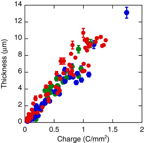
The amount of charge transferred during the anodization process could be calculated by integrating the current curves shown in figure (a-2) with respect to time. As can be seen from figure (a-2), the currents for all the applied voltages increased dramatically early in the anodization process and became constant after a while. As a result, the charge transferred was almost proportional to the anodization time. Figure shows the total thicknesses of the films with laminated structures plotted against the charge per unit area of the films. The overall thicknesses were approximately proportional to the total charge. That the values were distributed might be a result of minor factors such as the differences in the maximum currents or rates of decrease of the voltage. It is known to change the wave functions because of the generation of hydrogen gas during the ac anodization process; this affects the current curves [Citation84, Citation95]. The changes in the waveform of the current curves due to hydrogen gas also affect the amount of charge transferred; however, these factors were not considered at this stage because the effect of the waveform on the total overall charge transferred was assumed to be quite small.
Figure 7 Total thicknesses of the laminated alumina films versus the charge transferred per unit area: •: 0.3 mol l−1 sulfuric acid, •: 0.3 mol l−1 oxalic acid and •: 0.3 mol l−1 phosphoric acid.
Formation mechanism of laminated structures by ac anodization
On the basis of these results, we propose the following mechanism for the formation of the laminated structure observed in the alumina films grown via ac anodization. At the anode, alumina is formed by the oxidation of aluminum in the same manner as occurs during anodic dc oxidation
(1)
During the early stages of dc anodization, numerous small-diameter pre-pores are known to form on the surface of the growing alumina film. Generally, over time, these pre-pores decrease in number, and the diameters of the pre-pores that remain increase. This results in the formation of nanoholes [Citation108, Citation109]. It has been reported that the formation of both pre-pores and nanoholes can be controlled by controlling the experimental conditions [Citation106]. Some of these pre-pores increase in size and become holes. The sizes of these holes are typically 12 nm in the case of sulfuric acid [Citation1], approximately 25 nm in the case of oxalic acid [Citation109] and 33 nm in the case of phosphoric acid [Citation1]. The pre-pores are enlarged owing to the dissolution of the alumina in the acidic electrolyte.
During the cathode reaction, hydrogen is generated at the surface of the aluminum sheet. The two possible reactions for the formation of hydrogen are as follows:
(2)
(3)
It is likely that H+ ions or H2O are transported across the alumina film through weak spots such as pores and flaw sites [Citation74, Citation110] and reduced to hydrogen at the interface between the alumina layer and the aluminum sheet. It is also possible that the H+ ions are reduced more readily (reaction (Equation2(2) )) when their concentrations are high. However, considering that the standard electrode potential of reaction (Equation3
(3) ) is −0.828 V, a value lower than that for reaction (Equation2
(2) ), which is 0 V [Citation111], reaction (Equation3
(3) ) would occur more readily than reaction (Equation2
(2) ). At the same time, the OH− ions react with the Al ions formed during the anode reaction (equation (Equation1
(1) )). This results in the chemical etching of the alumina film at the weak spots via the reaction given below:
Hence, the pH does not change in this reaction. It is also possible that the OH− ions react with H+ ions as follows:
When the cathode reaction is repeated, the generated hydrogen increases the pressure at the interface between the alumina film and the Al sheet, resulting in the exfoliation of the alumina film from the surface of the aluminum sheet and the liberation of hydrogen gas. After the anode and cathode reactions have occurred numerous times, the alumina film separates completely.
Following the exfoliation of the top layer, the freshly exposed surface is anodized again and new alumina layers are formed via the same process. Once the second layer has formed, the layers beneath it peel off from the aluminum sheet when the thickness of the layer reaches a value on the order of 50–200 nm, and a new layer is formed.
The second and third layers were formed approximately 10 s after the growth of the top layer. This suggests that the alumina films were not formed through a single anode reaction (i.e. in 1/50 s) but grew over a number of instances of the reaction. We intend to study the mechanism in greater detail by employing ac frequencies other than 50 Hz.
In the case of dc anodization, the thickness of the barrier layer is proportional to the applied voltage and their ratio is usually called the anodization ratio; this parameter depends on the electrolyte used. In the alumina film, ionic conduction is predominant and the film is formed according to reaction (1), although both electrons and ions are involved in conduction at high electric fields. Hence, the thickness of the barrier layer is dependent on and proportional to the dc voltage [Citation107]. Similarly, it can also be concluded that the thicknesses of the individual layers are proportional to the ac voltage during the ac anodization process.
Biomimetic formation of nacre structure of shells by ac anodization
The laminated layer structures fabricated by ac anodization resembled tiled aragonite and were similar to the nacre produced by shells. In recent years, the mimetic construction of natural biogenic structures has attracted significant interest and inspired new knowledge [Citation112–Citation115]. Nacre structures, which have periodic bricks-and-mortar arrangements, are also of interest because of their high mechanical strength and unusual, structurally induced optical properties [Citation113, Citation116, Citation117]. Thus, the large-scale preparation of artificial nacre structures has become a research focus. The tiled aragonite structure in nacre is formed by CaCO3, which is observed in most shells, and several attempts have been made to prepare nacre structures from this mineral [Citation118–Citation120]. However, it is difficult to prepare CaCO3, and thus, various structural substitutes have been proposed, including clay platelets such as montmorillonite [Citation121–Citation123] and Al2O3 [Citation124], graphene or graphene oxide sheets [Citation125, Citation126], metal oxide nanosheets [Citation127] and layered double-hydroxide platelets [Citation128]. Our data suggested that ac anodization might be a plausible technique to prepare nacre structures from alumina. In detail, the nacre structures may be distinguished into two types: a tiled structure with a smooth surface observed in bivalves, and a tiled structure with terraced cones observed in spiral shells. The terraced cones are observed in the spiral-shaped shells of abalones [Citation129–Citation131] or gastropods [Citation132].
From ac anodization, laminated structures were obtained which resembled the flat tile structures (described above). Laminated structures with terraced cones could also be fabricated by controlling the anodization conditions.
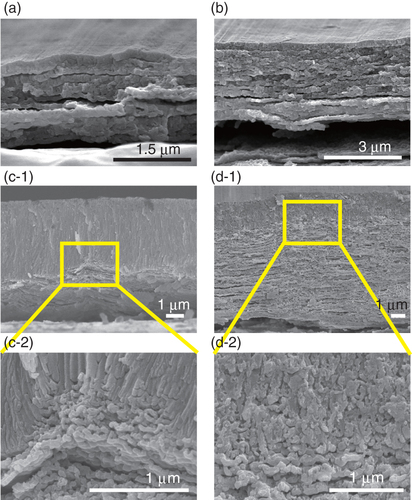
Figure shows SEM images of the films prepared at 50 V in sulfuric acid for 600 s. The concentration of sulfuric acid was 0.1 mol l−1 for the films in (a) and (b) and 0.75 mol l−1 for the films in (c) and (d). The rate of increase was 0.1 V s−1 for the films in (a) and (c), and 1 V s−1 for the films in (b) and (d). The total thickness increased with increases in the concentration of sulfuric acid and the rate of increase, because the amount of charge transferred increased. When the concentration was 0.75 mol l−1, the thickness of the top layer, which contained perpendicular, columnar structures, was greater than those of the layers formed at 0.1 mol l−1. In particular, the top layer was much thicker when the rate of increase was 0.1 V s−1, as shown in (c). Furthermore, the sample shown in (c) had a laminated structure with terraced cones, which represent the convex interface between the laminated portion and the columnar portion. These structures were similar to those observed in the spiral-shaped shells of abalones [Citation129–Citation131] and gastropods [Citation132]. A magnified SEM image of a terraced cone showed that partial, laminated layers were formed in the higher portions of the cone. As mentioned, the top layer was formed first, and the laminated layers were formed next. During the formation of the laminated layers, the terraced cones started to form more readily in the portions of the laminated structure that corresponded to nanopores or flaw sites [Citation74, Citation110] than in the other regions. The formation of the terraced cones took place in sulfuric acid solutions with concentrations higher than 0.6 mol l−1 for voltage increase rates lower than 0.2 V s−1. When the concentration was greater than 0.9 mol l−1, the alumina film was exfoliated from the aluminum sheet, and the voltage could not be applied. This suggested that the concentration of sulfuric acid and the rate of increase of the voltage affected the formation of the terraced cones. In particular, the thickness of the top layer increased for lower rates of voltage increase, and the terraced cones were formed when the thickness of the top layer was more than 2 μm. This means that the nanopores or flaw sites were limited in their ability to allow hydrogen molecules to pass as the top layer increased in thickness, and the formation of the laminated structure started at these sites with limited permeability.
Figure 8 Cross-sectional SEM images of the alumina films prepared at 50 V for an anodization time of 600 s in 0.1 mol l−1 sulfuric acid ((a) and (b)) and in 0.75 mol l−1 ((c) and (d)). The rate of increase of the voltage was 0.1 V s−1 ((a) and (c)) and 1 V s−1 ((b) and (d)). The images in (c-2) and (d-2) are the magnified versions of the ones in (c-1) and (d-1).
Conclusions
Ac anodization techniques of aluminum sheets were introduced in this review. Laminated alumina films could be fabricated via an ac anodization process. The morphologies of the films were affected by the applied potential, which depended on the nature of the electrolyte. The overall thicknesses of these alumina films increased as the total applied charge was raised, and the individual layer thickness also increased with the applied ac voltage, although it showed very little variation with respect to changes in the anodization time. Based on these results, the process involved in layer formation was proposed. The early stage of this proposed process involved the formation of an alumina barrier layer via the anode reaction, similar to the dc anodization process. Subsequently, hydrogen gas was generated, the alumina layer separated from the bulk aluminum, and anodic oxidation restarted over the freshly exposed surface.
The laminated layers were similar in structure to nacre, and ac anodization has potential in biomineralization. Two types of nacre structures are known. Differences in structure were demonstrated by controlling the rate of increase of the applied potential. Thus, laminated structures with terraced cones, which resemble the nacre structures observed in spiral shells, were obtained when the voltage rate increase was slow and the top layer was thicker than 2 μm.
References
- KellerFHunterM SRobinsonD L 1953 J. Electrochem. Soc. 100 411 10.1149/1.2781142
- MasudaHFukudaK 1995 Science 268 1466 10.1126/science.268.5216.1466
- MasudaMSatohM 1996 Japan. J. Appl. Phys. 35 L126 10.1143/JJAP.35.L126
- MasudaMYadaKOsakaA 1998 Japan. J. Appl. Phys. 37 L1340 10.1143/JJAP.37.L1340
- OnoSSaitoMIshiguroMAsohH 2004 J. Electrochem. Soc. 151 B473 10.1149/1.1767838
- LiuN WDattaALiuC YWangY L 2003 Appl. Phys. Lett. 82 1281 10.1063/1.1555689
- MasudaHMatsuiYYotsuyaMMatsumotoFNishioK 2004 Chem. Lett. 33 584 10.1246/cl.2004.584
- KimJHanHKimY HChoiS HKimJ CLeeW 2011 ACS Nano 5 3222 10.1021/nn2003458
- WhitneyT MJiangJ SSearsonP CChienC L 1993 Science 261 1316 10.1126/science.261.5126.1316
- NielschKMullerFLiA PGoseleU 2000 Adv. Mater. 12 582 10.1002/(SICI)1521-4095(200004)12:8%3C582::AID-ADMA582%3E3.0.CO;2-3
- ChuS ZWadaKInoueSTodorokiSTakahashiY KHonoK 2002 Chem. Mater. 14 4595 10.1021/cm020272w
- ChuS ZInoueSWadaKKurashimaK 2005 Electrochim. Acta 51 820 10.1016/j.electacta.2005.03.075
- ChuS ZInoueSWadaKKurashimaK 2004 J. Phys. Chem. B 108 5582 10.1021/jp0378642
- FriedmanA LMenonL 2007 J. Electrochem. Soc. 154 E68 10.1149/1.2509685
- OshimaHKikuchiHNakaoHMorikawaTMatsumotoKNishioKMasudaHItohK 2005 Japan. J. Appl. Phys. 44 L1355 10.1143/JJAP.44.L1355
- YasuiKMorikawaTNishioKMasudaH 2005 Japan. J. Appl. Phys. 44 L469 10.1143/JJAP.44.L469
- PeranioNLeisterETöllnerWEiblONielschK 2012 Adv. Funct. Mater. 22 151 10.1002/adfm.201101273
- SanderM SPrietoA LGronskyRSandsTStacyA M 2002 Adv. Mater. 14 665 10.1002/1521-4095(20020503)14:9%3C665::AID-ADMA665%3E3.0.CO;2-B
- DaiJ HLiuQWangLWuP WHuangXZhuZ BTianJ T 2013 Mater. Lett. 107 333 10.1016/j.matlet.2013.06.032
- CaoHQuiXLuoBLiangYZhangYTanRZhaoMZhuQ 2004 Adv. Funct. Mater. 14 243 10.1002/adfm.200305033
- NorekMŁukaGGodlewskiMPłocińskiTMichalska-DomańskaMWojciechJStępniowskiW J 2013 Appl. Phys. A 111 265 10.1007/s00339-012-7462-9
- HuangC HLinH YTzengYFanC HLiuC YLiC YHuangC WChenN KChuiH C 2012 Sensors Actuators A 180 49 10.1016/j.sna.2012.04.001
- KurowskaEBrzózkaAJaroszMSulkaG DJaskulaM 2013 Electrochim. Acta 104 439 10.1016/j.electacta.2013.01.077
- SulkaG DHnidaKBrzózkaA 2013 Electrochim. Acta 104 536 10.1016/j.electacta.2012.12.064
- MarichyCBechelanyMPinnaN 2012 Adv. Mater. 24 1017 10.1002/adma.201104129
- MubeenSSinghNLeeJStuckyG DMoskovitsMMcFarlandE W 2013 Nano Lett. 13 2110 10.1021/nl400502u
- ChuS ZInoueSWadaKHishitaSKurashimaK 2005 Adv. Funct. Mater. 15 1343 10.1002/adfm.200400253
- FoongT R BShenYHuXSellingerA 2010 Adv. Funct. Mater. 20 1390 10.1002/adfm.200902063
- GaoXChenJYuanC 2013 J. Power Sources 240 503 10.1016/j.jpowsour.2013.04.037
- ChuS ZWadaKInoueSHishitaSKurashimaK 2003 J. Phys. Chem. B 107 10180 10.1021/jp0354503
- ZhangMBandoYWadaKKurashimaK 1999 J. Mater. Soc. Lett. 18 1911 10.1023/A:1006664711344
- ChuS ZWadaKInoueSTodorokiS 2002 Chem. Mater. 14 266 10.1021/cm0105918
- BaoJTieCXuZMaQHongJSangHShengD 2002 Adv. Mater. 14 44 10.1002/1521-4095(20020104)14:1%3C44::AID-ADMA44%3E3.0.CO;2-K
- LiY LTangS LXieRWangYYangMGaoJ LXiaW BDuY W 2012 Appl. Phys. Lett. 100 052402 10.1063/1.3681136
- LüRZhouWShiKYangYWangLPanKTialCRenZFuH 2013 Nanoscale 5 8569 10.1039/c3nr01903a
- CheG LLakshmiB BFisherE RMartinC R 1998 Nature 393 346 10.1038/30694
- DongZZhouCChengHZhaoYHuCChenNZhanZLuoHQuL T 2013 Carbon 64 507 10.1016/j.carbon.2013.07.108
- ChuS ZWadaKInoueS 2002 Adv. Mater. 14 1752 10.1002/1521-4095(20021203)14:23%3C1752::AID-ADMA1752%3E3.0.CO;2-1
- MasudaHYanagishitaTYasuiKNishioKYagiIRaoT NFujishimaA 2001 Adv. Mater. 13 247 10.1002/1521-4095(200102)13:4%3C247::AID-ADMA247%3E3.0.CO;2-H
- HulteenJ CMartinC R 1997 J. Mater. Chem. 7 1075 10.1039/a700027h
- LakshmiB BDorhoutP KMartinC R 1997 Chem. Mater. 9 857 10.1021/cm9605577
- LakshmiB BPatrissiC JMartinC R 1997 Chem. Mater. 9 2544 10.1021/cm970268y
- KasugaTHiramatsuMHosonASekinoTNiiharaK 1998 Langmuir 14 3160 10.1021/la9713816
- ZhangMBandoYWadaK 2001 J. Mater. Sci. Lett. 20 167 10.1023/A:1006739713220
- ImaiHTakeiYShimizuKMatsudaMHirashimaH 1999 J. Mater. Chem. 9 2971 10.1039/a906005g
- ImaiHMatsudaMShimizuKHirashimaHNegishiN 2000 J. Mater. Chem. 10 2005 10.1039/b004543h
- HoyerPMasudaH 1996 J. Mater. Sci. Lett. 15 1228 10.1007/BF00274383
- KumeriaTLosicD 2012 Nanoscale Res. Lett. 7 88 10.1186/1556-276X-7-88
- YuZ G 2013 Appl. Phys. A 110 35 10.1007/s00339-012-7410-8
- MozalevAMagainoSImaiH 2001 Electrochim. Acta 46 2825 10.1016/S0013-4686(01)00497-2
- ChuS ZInoueSWadaKLiDSuzukiJ 2005 Langmuir 21 8035 10.1021/la050902j
- ChuS ZInoueSWadaKLiDHanedaH 2003 J. Mater. Chem. 13 866 10.1039/b211492e
- MartinC R 1994 Science 266 1961 10.1126/science.266.5193.1961
- ThormannATeuscherNPfannmollerMRotheUHeilmannA 2007 Small 3 1032 10.1002/smll.200600582
- HanaokaTHeilmannAKrollMKormannHSawitowskiTSchmidGJutziPKlippAKreibigUNeuendorfR 1998 Appl. Organometallic Chem. 12 367 10.1002/(SICI)1099-0739(199805)12:5%3C367::AID-AOC732%3E3.0.CO;2-Y
- MatsumotoFNishioKMasudaH 2004 Adv. Mater. 16 2105 10.1002/adma.200400360
- YanagishitaTYasuiKKondoTKawamotoYNishioKMasudaH 2007 Chem. Lett. 36 530 10.1246/cl.2007.530
- NagauraTTakeuchiFYamauchiYWadaKInoueS 2008 Electrochem. Commun. 10 681 10.1016/j.elecom.2008.02.012
- NagauraTTakeuchiFInoueS 2008 Electrochim. Acta 53 2109 10.1016/j.electacta.2007.09.016
- NagauraTWadaKInoueS 2010 Mater. Trans. 51 1237 10.2320/matertrans.M2010071
- KrishnanRThompsonC V 2007 Adv. Mater. 19 988 10.1002/adma.200601555
- HoA Y YGaoHLamY CRodríguezI 2008 Adv. Funct. Mater. 18 2057 10.1002/adfm.200800061
- LosicDLilloMLosicDJr 2009 Small 5 1392 10.1002/smll.200801645
- LosicDLosicDJr 2009 Langmuir 25 5426 10.1021/la804281v
- LeeWScholzRGöseleU 2008 Nano Lett. 8 2155 10.1021/nl080280x
- LeeWKimJ CGöseleU 2010 Adv. Funct. Mater. 20 21 27 21–7 10.1002/adfm.200901213
- MengG WJungY JCaoAVajtaiRAjayanP M 2005 Proc. Natl Acad. Sci. USA 102 7074 10.1073/pnas.0502098102
- ChenBXuQZhaoXZhuXKongMMengG 2010 Adv. Funct. Mater. 20 3791 10.1002/adfm.201001190
- ZaraskaLKurowskaESulkaG DJaskułaM 2012 J. Solid State Electrochem. 16 3611 10.1007/s10008-012-1795-3
- KatsutaYYasumoriAWadaKKurashimKSueharaSInoueS 2008 J Non-Cryst. Solids 354 451 10.1016/j.jnoncrysol.2007.06.085
- WadaKSotomuraTTsutsumiM 1994 J. Surf. Finishing Soc. Japan 45 112 10.4139/sfj.45.112
- KapeJ M 1977 Trans. Inst. Met. Finish. 55 25
- OnoSSatoT 1981 J. Surf. Finish. Soc. Jpn 32 184 10.4139/sfj1950.32.184
- GraeveI DTerrynHThompsonG E 2006 Electrochim. Acta 52 1127 10.1016/j.electacta.2006.07.010
- FotinoM 1993 Rev. Sci. Instrum. 64 159 10.1063/1.1144419
- ThompsonG EWoodG C 1978 Corros. Sci. 18 721 10.1016/S0010-938X(78)80092-4
- LeaversPTerrynHVereeckenJKernigBGrzembaB 1996 Corros. Sci. 38 413 10.1016/0010-938X(96)00135-7
- GoodD 1997 J. Electrochem. Soc. 144 1965 10.1149/1.1837730
- LaeversPHubinATerrynHVereechenJ 1998 J. Appl. Electrochem. 28 387 10.1023/A:1003288305367
- LinC SChangC CFuH M 2001 Mater. Chem. Phys. 68 217 10.1016/S0254-0584(00)00366-7
- TomasoniFParysHTerrynHHubinADeconinckJBuchlinJ MBeeckJ 2010 Electrochem. Commun. 12 156 10.1016/j.elecom.2009.11.012
- DimogerontakisTTerrynH 2007 Corros. Sci. 49 3428 10.1016/j.corsci.2007.03.009
- OnoSHabazakiH 2009 Corros. Sci. 51 2364 10.1016/j.corsci.2009.06.021
- NicklenD A LGabeD R 1978 Surf. Technol. 7 353 10.1016/0376-4583(78)90033-X
- BarbosaM AGabeD RRossD HSutherlandI 1989 J. Appl. Electrochem. 19 829 10.1007/BF01007930
- GabeD RDowtyI H 1987 Surf. Coat. Technol. 30 309 10.1016/0257-8972(87)90088-0
- WitH JBootsH M J 1983 J. Appl. Phys. 54 2727 10.1063/1.332299
- QuangK VBrindelFLaslazGButtoudinR 1983 J. Electrochem. Soc. 130 1248 10.1149/1.2119934
- JeongJ HKimS SKimH GChoiC HLeeD N 1996 Mater. Sci. Forum 217–222 1565 10.4028/www.scientific.net/MSF.217-222.1565
- LinC SLiW J 2006 J. Electrochem. Soc. 153 C51 10.1149/1.2131830
- DyerC KAlwittR S 1981 J. Electrochem. Soc. 128 300 10.1149/1.2127408
- LinC FPorterM DHerbertK R 1994 J. Electrochem. Soc. 141 96 10.1149/1.2054716
- LinC FHerbertK R 1994 J. Electrochem. Soc. 141 104 10.1149/1.2054667
- WangM HHerbertK R 1996 J. Electrochem. Soc. 143 2827 10.1149/1.1837114
- BargeronC BGivensR B 1977 J. Electrochem. Soc. 124 1845 10.1149/1.2133173
- NatishanP MMcCaffertyE 1989 J. Electrochem. Soc. 136 53 10.1149/1.2096613
- RyanR LMcCaffertyE 1995 J. Electrochem. Soc. 142 2594 10.1149/1.2050059
- OnoSHabazakiH 2010 Corros. Sci. 52 2164 10.1016/j.corsci.2010.02.039
- TerrynHVereeckenJThompsonG E 1991 Corros. Sci. 32 1173 10.1016/0010-938X(91)90130-H
- HammonsJ ARaymentTTzedakiMIngelgemY VUstarrozJVandendaelIHubinATerrynH 2012 Electrochim. Acta 70 10 10.1016/j.electacta.2012.02.083
- TrevertonJ ADaviesN C 1980 Electrochim. Acta 25 1571 10.1016/0013-4686(80)80006-5
- BalasubramanianVJohnSShenoiB A 1983 Surf. Technol. 19 293 10.1016/0376-4583(83)90034-1
- SegawaHOkanoHWadaKInoueSByunI 2013 J. Electrochem. Soc. 160 D240 10.1149/2.108306jes
- SegawaHOkanoHWadaKInoueS 2011 Electrochem. Solid State Lett. 44 C13 10.1149/1.3607297
- ChuS ZWadaKInoueSIsogaiMKatsutaYYasumoriA 2006 J. Electrochem. Soc. 153 B384 10.1149/1.2218822
- OhJThompsonC V 2011 Electrochim. Acta 56 4044 10.1016/j.electacta.2011.02.002
- DiggleJ WDownieT CGouldingC W 1969 Chem. Rev. 69 365 10.1021/cr60259a005
- FukudaYFukushimaT 1980 Bull. Chem. Soc. Japan 53 3125 10.1246/bcsj.53.3125
- FukudaY 1974Nippon Kagaku Kaishi 1974 1968 10.1246/nikkashi.1974.1868
- TakahashiHKasaharaKFujiwaraKSeoM 1994 Corros. Sci. 36 677 10.1016/0010-938X(94)90073-6
- The Electrochemical Society of Japan Handbook of Electrochemistry 2000 5th edn Maruzen 92 95 pp 92–5
- HuebschNMooneyD J 2009 Nature 462 426 10.1038/nature08601
- AksayI ATrauMManneSHonmaIYaoNZhouLFenterPEisenbergerP MGrunerS M 1996 Science 273 892 10.1126/science.273.5277.892
- SellingerAWeissP MNguyenALuYAssinkR AGongWBrinkerC J 1998 Nature 394 256 10.1038/28354
- EhrlichHDemadisK DPokrovskyO SKoutsoukosP G 2010 Chem. Rev. 110 4656 10.1021/cr900334y
- MeyersM AChenP YLinA Y MSekiY 2008 Prog. Mater. Sci. 53 1 10.1016/j.pmatsci.2007.05.002
- MannS 1988 Nature 332 119 10.1038/332119a0
- LiX QZengH C 2012 Adv. Mater. 24 6277 10.1002/adma.201202733
- SuzukiMSaruwatariKKogureTYamamotoYNishimuraTKatoTNagasawaH 2009 Science 325 1388 10.1126/science.1173793
- KatoT 2000 Adv. Mater. 12 1543 10.1002/1521-4095(200010)12:20%3C1543::AID-ADMA1543%3E3.0.CO;2-P
- TangZKotovN AMagonovSOzturkB 2003 Nature Mater. 2 413 10.1038/nmat906
- PodsiadloP 2007 Science 318 80 10.1126/science.1143176
- WaltherABjurhagerIMalhoJ MPereJRuokolainenJBerglundL AIkkalaO 2010 Nano Lett. 10 2742 10.1021/nl1003224
- BondererL JStudartA RGaucklerL J 2008 Science 319 1069 10.1126/science.1148726
- RaoC N RSoodA KSubrahmanyamK SGovindarajA 2009 Angew. Chem. Int. Edn Engl. 48 7752 10.1002/anie.200901678
- DikinD AStankovichSZimneyE JPinerR DDommettG H BEvmenenkoGNguyenS TRuoffR T 2007 Nature 448 457 10.1038/nature06016
- OsadaMSasakiT 2009 J. Mater. Chem. 19 2503 10.1039/b820160a
- YaoH BFangH YWangX HYuS H 2011 Chem. Soc. Rev. 40 3764 10.1039/c0cs00121j
- LinAMeyersM A 2005 Mater. Sci. Eng. A 390 27 10.1016/j.msea.2004.06.072
- EvansA FSuoZWangR ZAksayI AHeM YHutchinsonJ W 2001 J. Mater. Res. 16 2475 10.1557/JMR.2001.0339
- WangR ZSuoZEvansA FYaoNAksayI A 2001 J. Mater. Res. 16 2485 10.1557/JMR.2001.0340
- FritzMBeichermA MRadmacherMWaltersP KHansmaP KStuckyG DMorseD EMannS 1994 Nature 371 49 10.1038/371049a0